Article

Research on the Correlation of Physical Properties Between NbN Superconducting Thin Films and Substrates

Institute of Next Generation Semiconductor Materials, Southeast University, Suzhou 215123, China
*
Author to whom correspondence should be addressed.
Coatings 2025, 15(5), 513; https://doi.org/10.3390/coatings15050513
Submission received: 24 March 2025 / Revised: 17 April 2025 / Accepted: 22 April 2025 / Published: 24 April 2025
(This article belongs to the Special Issue Electrochemical Properties and Applications of Thin Films)

Abstract

:
This paper investigates the relationship between the physical properties of NbN thin films and a series of different substrates/buffer layers used for the thin film growth. Substrates, including 4H-SiC, AlN/Si, AlN/sapphire, and annealed AlN/sapphire, were selected for NbN film deposition via DC magnetron sputtering. Post-deposition annealing was also employed to study its impact on the films’ quality. Comprehensive characterizations were performed on NbN films, focusing on superconducting critical temperature (TC), transition width (ΔTC), crystalline quality, and surface roughness. The results demonstrate that the annealed NbN films grown on 4H-SiC substrates with the highest crystalline quality exhibit optimal crystalline quality, achieving a TC of 16.3 K. Experimental results reveal intrinsic correlations between the critical properties of NbN superconducting thin films and substrate structural characteristics; the impact of post-growth annealing on the TC is also studied.

1. Introduction

NbN thin films exhibit exceptional properties including high superconducting critical temperature [1], short coherence length [2], excellent chemical stability [3], large critical current [4], and short electron–phonon interaction time in the superconducting state [5]. These superior characteristics have enabled the widespread application of NbN films in superconducting devices such as superconducting nanowire single-photon detectors (SNSPDs) [6], kinetic inductance detectors (KIDs) [7], superconductor-insulator-superconductor (SIS) tunnel junction mixers and hot-electron bolometer (HEB) mixers [8,9]. The crystalline phases of NbN are primarily classified into seven categories, among which δ-NbN with a face-centered cubic (FCC) structure demonstrates enhanced TC values in thin film form [10].
The improvement of the refrigeration limit and temperature maintenance capacity of cryogenic systems is often accompanied by a significant increase in energy consumption, cost, and footprint. Therefore, superconducting devices should be designed to operate at relatively elevated environmental temperatures, to avoid such waste [11]. Owing to its higher theoretical TC upper limit (about 18 K [12]), NbN thin films demonstrate greater research significance and broader application prospects. Current research findings indicate that the TC of NbN films can be progressively optimized through substrate/buffer layer selection, process parameter adjustment, and post-growth techniques such as annealing at appropriate temperatures.
NbN film fabrication is typically achieved via high-temperature chemical vapor deposition (CVD) and radio-frequency (RF) magnetron sputtering [13,14]. Previous studies have established that desired TC can be obtained within a specific thin film thickness range, and it is observed that TC increases significantly with the increase in film thickness [15]. Researchers attribute this enhancement to reduced disorder and grain boundary defects as thickness increases [2]. However, when film thickness exceeds a critical value (about 50 nm), further thickness variations exhibit negligible influence on TC [16]. Notably, film thickness must be constrained within process-compatible limits during device fabrication, rendering thickness escalation as a TC-enhancement strategy potentially impractical.
In the growth of NbN thin films, the selection of substrates and buffer layers plays a critical role in determining film properties. Significant lattice mismatch exists between conventional substrates (such as Si) and NbN films, with mismatches of 19% for Si/δ-NbN. Thinner NbN films grown on Si substrates generally exhibit TC values not exceeding 12 K. To date, the highest reported TC for NbN layers directly grown on Si substrates is only 15.3 K, achieved in a 180 nm thick sample [17]. To mitigate lattice mismatch, alternative substrate materials with closer lattice parameters to NbN have been explored, including MgO [18], III-nitride materials [19], and sapphire [20]. The NbN thin films with a thickness below 10 nm grown on these substrates exhibit a TC exceeding 12 K. However, except for sapphire, these substrates are generally cost-prohibitive for industrial-scale applications. Consequently, sapphire has become the predominant substrate for NbN film production.
To achieve enhanced lattice matching while maintaining cost efficiency, researchers have introduced buffer layers such as AlN (Preferred Orientation), TiN, and AlGaN between Si substrates and NbN films [11,21,22]. Under specified process conditions, these buffer layers enhance the TC of NbN thin films by 1–5 K compared to bare silicon substrates. Nevertheless, as epitaxial crystalline films themselves, buffer layers inherently contain structural defects. The potential impact of these intrinsic defects on subsequently deposited NbN films remains unexplained.
Post-growth annealing, a well-established post-processing method for improving film crystallinity [23], functions to repair crystal damage and relieve internal stresses. In this study, we implement high-temperature annealing to engineered buffer layers with varying crystalline qualities. Subsequently, NbN films are deposited under identical sputtering parameters on both bare and buffered substrates (collectively referred to as "substrates" hereafter). Through systematic characterization, we analyze the correlation between substrate crystalline quality and the TC of the NbN films.

2. Materials and Methods

To investigate the influence of crystalline quality in AlN buffer layers on subsequently deposited NbN films, we engineered buffer layers with controlled crystalline properties. The AlN buffer layers were deposited on silicon and sapphire substrates via metal-organic chemical vapor deposition (MOCVD), followed by characterization of surface roughness and crystal defect density. The MOCVD process proceeded as follows.
The pressure in the reaction chamber was first reduced to 5000 Pa. The substrate temperature was then raised to 900 °C, with the Si substrates oriented as Si(111) and sapphire substrates as Sapphire(001). After stabilizing the temperature at 900 °C to ensure uniform heating, ammonia (NH₃) and hydrogen (H2) were introduced at flow rates of 7000 sccm and 120 sccm, respectively, maintaining a chamber pressure of ~400 mbar. Subsequently, the substrates were cleaned with hydrogen at high temperature for 5 min. Following cleaning, the TMAl valve was opened, and TMAl was delivered into the chamber using hydrogen as the carrier gas. Under high-temperature conditions, TMAl reacted with ammonia to deposit AlN on the substrate surface over a 10-min period. All AlN films were grown to 200 nm thickness.
The resulting samples comprised 2 × AlN/Si (111) and 4 × AlN/c-sapphire. Subsequently, two AlN/sapphire specimens underwent post-deposition annealing in nitrogen ambient for buffer layer optimization.
The following parameters were employed for high-temperature annealing of the AlN buffer layer: temperature of 1550 °C, annealing duration of 1 h, vacuum level of 2 × 10⁻³ Pa, using a vertical annealing furnace. Due to the melting point of Si substrates (1414 °C) being incompatible with these annealing conditions, the process was exclusively applied to AlN on sapphire substrates. Figure 1 compares the XRD measurement results of the AlN buffer layer before and after annealing. A visual inspection of the curve profiles reveals that high-temperature annealing under optimal conditions significantly improves the crystalline quality of AlN.
The characterization results of different substrates and buffer layers are summarized in Table 1. Considering the non-uniformity of AlN films, where significant variations in root mean square (RMS) values may exist across different regions of the same sample, three randomly selected points in the central area of each sample were measured for RMS values, with the average value adopted as the final RMS of the sample. Detailed calculations are omitted here.
The edge dislocation density is calculated using the following Formula (1) [24]:
DE = βE2/(4.35 |bE2|)
where DE represents dislocation density, βE denotes the FWHM, and bE is the magnitude of the Burgers vector for dislocations. For AlN, bE is conventionally approximated as the lattice constant along its a-axis. Formula (1) demonstrates that a smaller FWHM value corresponds to a lower dislocation density.
It is observed that the high-temperature annealed AlN exhibits increased RMS roughness, while the full width at half maximum (FWHM) of the AlN (102) plane from rocking curve shows a notable reduction of 40%–50%. Since the FWHM of the (002) plane rocking curve mainly reflects screw dislocation density and that of the (102) plane mainly corresponds to edge dislocation density, the edge dislocation density in AlN buffer layers exerts greater influence on the continuity of epitaxial layers. Thus, the FWHM value of the (102) plane rocking curve is adopted as the metric for evaluating the crystalline quality of the buffer layer.
The AlN layers in this study were fabricated via MOCVD at a growth temperature of 900 °C. Prior to implementing the 1550°C annealing protocol, preliminary trials at 950 °C, 1050 °C, and 1250 °C were conducted. XRD characterization confirmed these lower-temperature annealing processes failed to improve crystalline quality, and thus their results are excluded from presentation. It is noted here that the annealing temperature of 1550 °C was selected with reference to Luo’s work [25].
Given the experimental objective focused on preparing AlN layers with deliberately varied crystalline qualities for qualitative comparison rather than determining optimal annealing parameters, the AlN annealing investigation was terminated upon successful preparation of the 1550 °C-annealed specimens.
The 4H-SiC substrate demonstrates comparably low lattice mismatch with NbN (4‰ vs. AlN/NbN mismatch of 3‰). As a commercialized substrate, it has superior crystalline quality and sub-nanometer surface roughness which is advantageous over epitaxy layers. Therefore, two additional 4H-SiC substrates were incorporated, yielding four experimental groups (eight substrates total).
NbN films were deposited using a DC-powered Lesker Proline PVD75 magnetron sputtering system under N2/Ar atmosphere. The vacuum chamber was initially evacuated to 4 × 10⁻⁷ Torr via cryopump. Substrates were preheated at 200 °C for 5 min prior to deposition. Process gases maintained chamber pressure at 3 mTorr with 18% N2/Ar ratio. A 150 W pre-sputtering step (5 min) cleansed the target surface, followed by 15 min main deposition under identical power. Post-growth characterization evaluated surface roughness, defect density, and TC. For each of the four substrate types, one NbN thin film specimen was selected and annealed at 900 °C under N2 atmosphere for 1 h (within a single batch process) to systematically investigate thermal processing effects. A total of 8 NbN thin film samples were prepared through the above process, with all sample names listed in Table 2. The suffix "-a" in the sample names indicates that the corresponding NbN underwent annealing treatment.
It should be noted that the aforementioned process parameters for magnetron sputtering and high-temperature annealing were reported by a previous study in which multiple sets of process parameters for magnetron sputtering and high-temperature annealing were reported [10].
Experimental Analysis Procedures:
  • Intra-Substrate Horizontal Comparison. Conducted cross-analysis of NbN film properties on identical substrates to evaluate annealing-induced optimization effects;
  • Longitudinal Contrast Studies. As-deposited Films: four-sample longitudinal comparison established substrate influence mechanisms on non-annealed NbN films. Annealed Films: parallel four-sample longitudinal comparison decoupled substrate effects in post-annealing scenarios;
  • Correlation and Modeling. Should significant correlations emerge: establish dominant mechanisms through statistical pattern recognition; perform curve fitting analyses using least squares regression; validate models via residual error minimization.
Characterization Methods: Surface roughness was measured using atomic force microscopy (AFM). Film thickness was determined via X-ray reflectivity (XRR) mode of an X-ray diffractometer, while crystal dislocation density was evaluated by X-ray diffraction (XRD) mode. The superconducting critical temperature of the films was assessed using a Physical Property Measurement System (PPMS). Table 3 summarizes the manufacturers and model numbers of the equipment employed, along with related specifications.
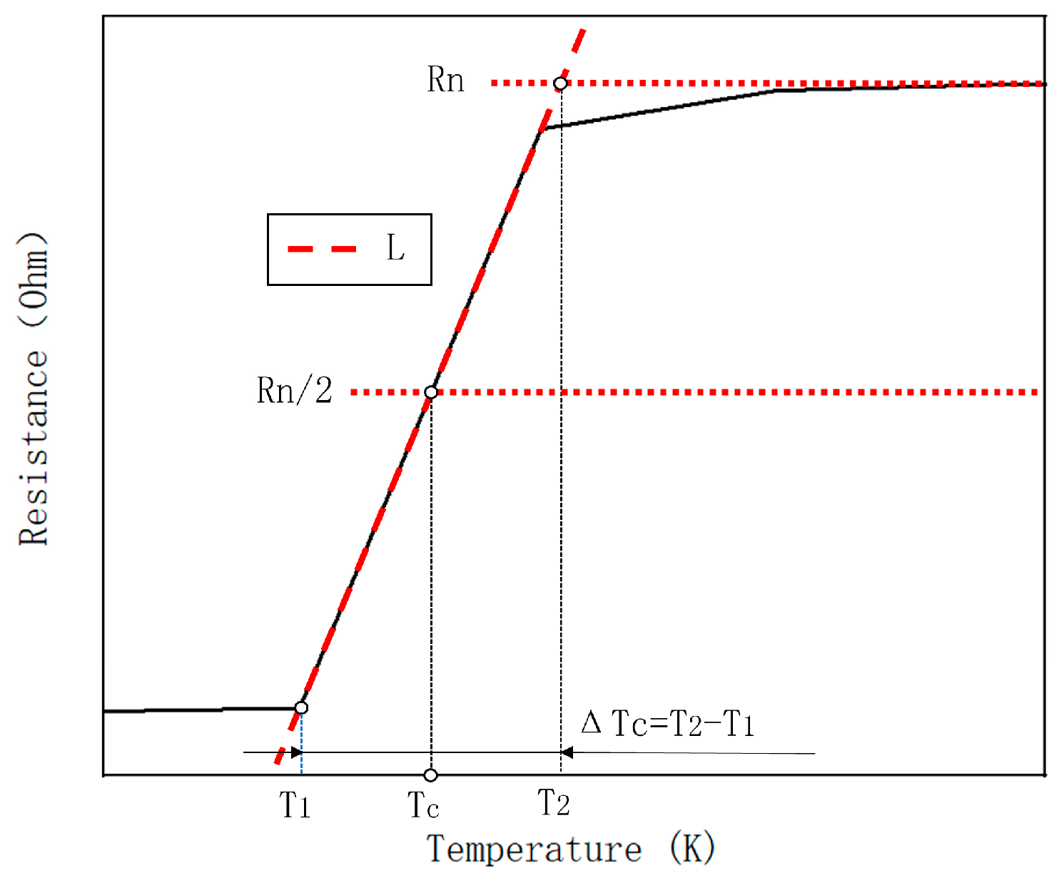
The transition of the superconducting sample’s resistance from the normal state to the superconducting state occurs over a finite temperature interval. The length of this interval is defined as the superconducting transition width, ΔTC, whose magnitude depends on factors such as material purity, crystalline integrity, and internal stress states of the sample. For superconducting thin films with a large ΔTC (≥10−3 K), the critical temperature TC is defined as the temperature at which the resistance drops to half of the normal-state resistance [26].
As the NbN thin films in this experiment are heteroepitaxial layers exhibiting compromised crystalline quality and intrinsic stress, the resistance does not follow a linear decay profile within the ΔTC transition range. The boundary points of the transition region cannot be unambiguously identified directly from the raw R-T curve. Therefore, the transition region endpoints are operationally defined by the intersection coordinates between the linear extrapolation (L) of the normal-state resistance (Rn) and the superconducting transition curve, while TC is determined by the intersection of L with Rn/2, as demonstrated in Figure 2.

3. Results and Discussion

3.1. Characterization Results

Table 4 summarizes the characterization results of superconducting critical temperature (TC), superconducting transition width (ΔTC), RMS, and full width at half maximum (FWHM) for various NbN samples. The results indicate that the TC of annealed NbN films exhibits significant correlation with the crystallinity of corresponding substrates, while as-deposited NbN films show potential correlation with substrate crystalline quality. High-temperature annealing with optimized parameters substantially enhances the TC of superconducting films and reduces ΔTC. As anticipated, NbN films grown on SiC substrates with the highest crystalline quality demonstrate excellent performance in both TC and ΔTC metrics. The NbN-SiC-a sample achieves a near-theoretical-limit Tc value of 16.3 K. According to conventional NbN fabrication experience, the TC of NbN films deposited directly on bare sapphire substrates under identical process parameters typically ranges from 9 to 10 K. Notably, all samples in this study exhibit TC values no less than 10 K, reaffirming that introducing a buffer layer between NbN films and substrates with high lattice mismatch constitutes an effective strategy for improving NbN film quality.
Figure 3 displays the Resistance-Temperature (R-T) curves of annealed and non-annealed NbN thin films on identical substrates. The annealed samples exhibit better TC and ΔTC compared to their non-annealed counterparts, providing direct visual evidence supporting the aforementioned conclusions.

3.2. Correlation Between TC of NbN Thin Films and Substrate Crystalline Quality

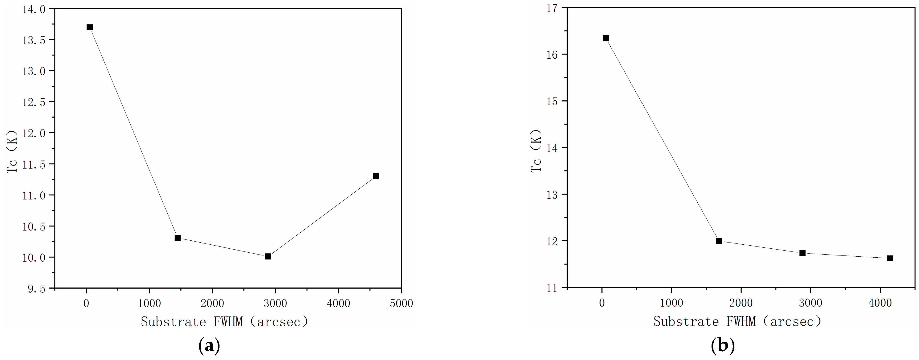
Figure 4 illustrates the correlation between the (102) plane FWHM of substrates and the TC of NbN films pre-/post-annealing. As shown in Figure 4a, the TC of as-deposited NbN films exhibits a latent dependence on substrate crystallinity, with the highest TC observed in films grown on the highest-quality substrate (4H-SiC). The non-monotonic relationship between NbN film TC and substrate FWHM implies additional influencing factors during film growth beyond substrate crystalline quality.
Based on prior observations, the observed phenomenon is hypothesized to originate from thermal mismatch between the AlN buffer layer and the substrate. The coefficients of thermal expansion (CTE) of AlN, Si, and sapphire are listed in Table 5. Before NbN film formation, the Si substrate exhibited a lower CTE than the AlN buffer layer, allowing the AlN crystal quality to remain unaffected by thermal mismatch. In contrast, the a-axis CTE of the sapphire substrate exceeded that of the AlN buffer layer, introducing additional dislocations in the AlN layer due to thermal mismatch. Concurrently, the enhanced lattice distortion induced by the AlN layer suppresses the preferred orientation growth of NbN, potentially leading to the presence of trace superconducting-inferior crystalline phases (e.g., ε-NbN). This dual mechanism results in lower TC values for NbN films deposited on AlN/Sapphire substrates than those on AlN/Si substrates. This is consistent with the research conclusions of Sui et al. regarding AlScN thin films [27].
In contrast, Figure 4b demonstrates that high-temperature annealing effectively mitigates residual film stress and reduces dislocation density. By eliminating process-dependent variables (all NbN films were fabricated in a single batch with identical N2/Ar ratios, temperature profiles, and deposition parameters), the intrinsic correlation between NbN films and their substrates/buffer layers becomes unequivocally apparent.
Critical analysis of Figure 4b reveals a deterministic relationship: substrates and buffer layers with lower FWHM values for the (102) plane exhibit reduced edge dislocation densities, which directly correlate with enhanced TC values in the overlying NbN films. This observation confirms that post-annealed NbN film properties are predominantly governed by the crystalline perfection of the underlying heterostructure.
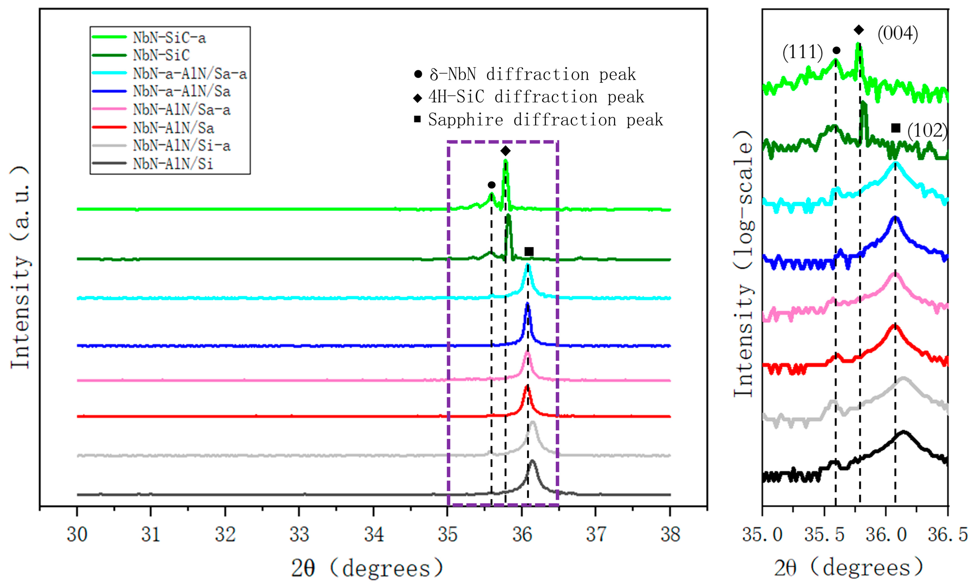
Figure 5 displays the X-ray ω-2θ scan curve of various NbN samples. All samples exhibit diffraction peaks with varying intensities near 2θ = 35.6°, whose positions closely align with the δ-NbN (111) reference peak (PDF# 00-038-1155). As no materials other than the substrate and NbN are detected, these diffraction peaks are conclusively identified as δ-NbN (111) reflections. The FWHM of δ-NbN (111) diffraction peaks, determined by profile analysis, serves as an indicator of NbN crystalline quality. These FWHM measurements are quantitatively presented in Table 4 for comprehensive comparison.
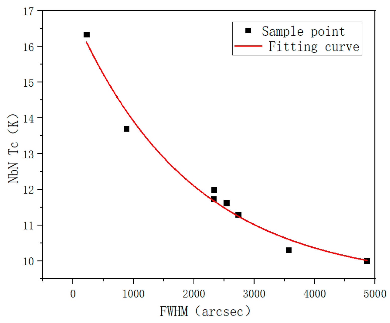
Figure 6 displays the correlation between the TC and FWHM of the NbN samples. A significant negative correlation between TC and β was observed. The NbN thin film exhibiting the lowest FWHM and highest TC was achieved on the 4H-SiC substrate with supreme crystalline quality.
For thin films with low dislocation densities, TC is highly sensitive to dislocation density, leading to a rapid TC decline in the low-FWHM regime. At higher dislocation densities, the superconducting coherence length becomes constrained, and the influence of dislocations on TC saturates, resulting in a reduced TC decline rate and stabilization in the high-FWHM regime. As previously mentioned, the strong correlation between film thickness and dislocation density inherently aligns the observed dislocation-density-dependent TC variation with the thickness-dependent TC evolution reported in reference [15].
Based on the above discussion, it can be seen that among the substrates with low lattice mismatch to NbN, those substrates with intrinsically low dislocation densities enable the propagation of reduced defect densities into the overlying epitaxial films. This defect suppression mechanism enhances crystalline perfection, which directly correlates with improved carrier mobility and superconducting coherence lengths. This conclusion aligns with established defect–property relationships observed in GaN epitaxial layers grown on AlN buffer systems, as reported in nitride semiconductor research [31].
Furthermore, when investigating the effects of other process parameters on film properties, inspired by the significant influence of substrate crystallinity on NbN’s electrical performance, we rigorously maintained comparable crystallinity levels across all substrates throughout the experiment in accordance with the principle of controlling variables, thereby eliminating substrate-induced interference in experimental results.

3.3. Correlation Analysis Between ΔTC and Thin Film FWHM

By examining the ΔTC and thin film FWHM data of various annealed NbN samples listed in Table 4, no evident correlation was observed between the two datasets. Since samples grown in the same batch eliminate potential variations in material purity, the magnitude of ΔTC is determined by the internal stress state and crystal dislocation density within the material [26]. This observation leads to the conclusion that residual stress exists within the samples.
In practical production, when targeted reduction of superconducting thin film ΔTC is required, beyond selecting substrates with matching coefficients of thermal expansion and optimized annealing parameters, supplementary stress-modulation techniques such as mechanical stretching might be implemented to mitigate adverse effects of internal stress on material performance.

3.4. Correlation Between NbN Thin Films and Substrate Surface Morphology

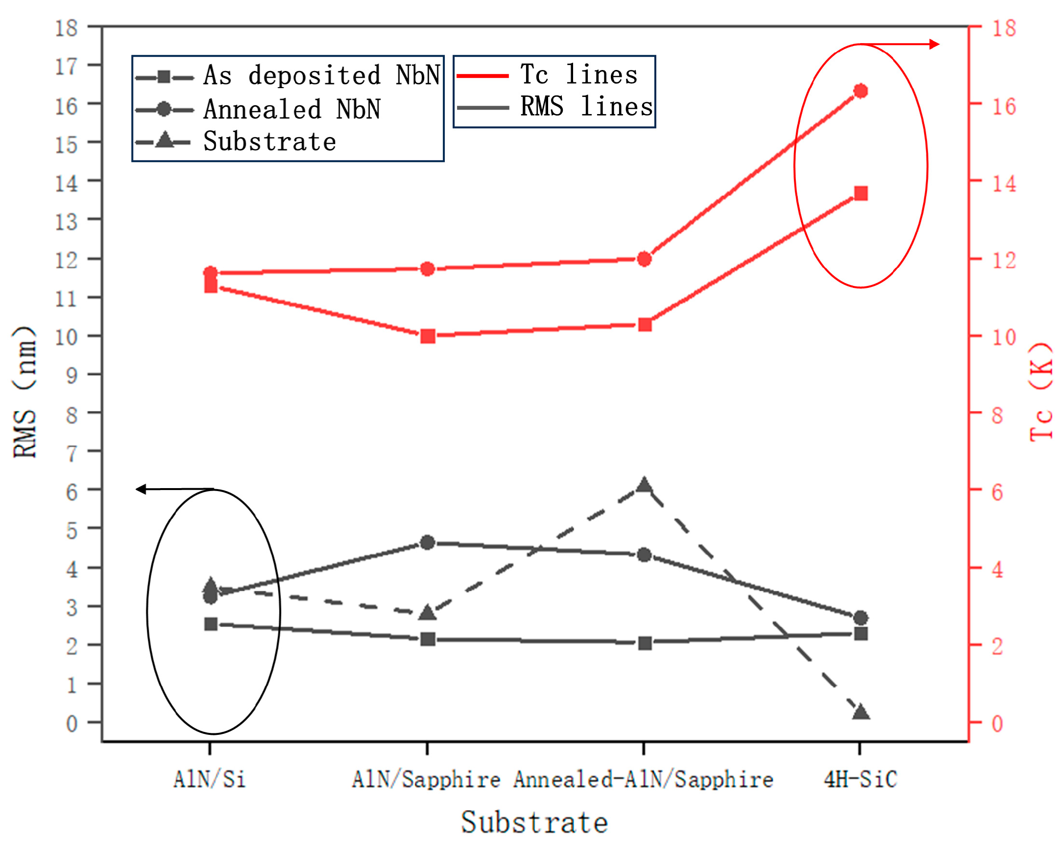
Figure 7 displays the surface RMS and TC values of substrates and NbN thin films before and after annealing. Analysis of all sample data reveals no significant correlation between thin film RMS and TC, regardless of annealing treatment. Additionally, no apparent correlation exists between thin film surface RMS and substrate surface RMS.
Table 6 shows the surface RMS values of all samples and their corresponding substrates. Given the clustered distribution of RMS values among substrates of identical material types, a rational data selection strategy was implemented for Figure 7 visualization: one representative substrate from each pair sharing identical material was retained for RMS data plotting. This approach effectively maintains analytical clarity while eliminating redundant data points, enabling unambiguous observation of intergroup relationships across different substrate categories.
Figure 8 shows the AFM characterization results of substrates and their corresponding thin films. Analysis of surface morphology in as-deposited samples reveals that although all films exhibit comparable RMS, the inherent micropore structures on substrates remain partially exposed. Even after high-temperature annealing treatment for film optimization, the influence of large-scale structural features (e.g., pre-existing voids or protrusions) originating from substrates cannot be fully eliminated.

4. Conclusions

For approximately 30 nm thick NbN films grown on substrates with similar lattice constants under identical process parameters, a significant correlation exists between the TC of NbN after annealing with optimized parameters and the crystalline quality of the substrate/buffer layer: lower FWHM corresponds to higher TC. This correlation was further observed between the TC of NbN films and their own XRD-FWHM. Theoretical analysis indicates that SIS tunnel junctions fabricated with NbN material (TC = 16.3 K) could achieve effective operating frequencies approaching 2 THz when operated at 5 K.
When film thickness reaches 30 nm, substrate surface roughness ≤6 nm exhibits negligible impact on film surface roughness or TC. However, macro-defects (e.g., micropores) on substrates propagate into epitaxial layers, necessitating defect screening in precision processing of epitaxial structures.
ΔTC characterization reveals persistent residual stress in annealed films, continuing to influence their physical properties. To further optimize ΔTC, supplementary stress-reduction techniques must be incorporated alongside annealing processes.

Author Contributions

Conceptualization, Z.H. and X.G.; methodology, Z.H.; validation, X.G., Q.F. and X.N.; investigation, Z.H.; resources, X.G., Q.F. and X.N.; data curation, Z.H., Y.P. and X.G.; writing—original draft preparation, Z.H.; writing—review and editing, X.G.; supervision, X.G.; project administration, X.G. All authors have read and agreed to the published version of the manuscript.

Funding

This research received no external funding.

Institutional Review Board Statement

Not applicable.

Informed Consent Statement

Not applicable.

Data Availability Statement

Data are contained within the article.

Conflicts of Interest

The authors declare no conflicts of interest.

References

  1. Cucciniello, N.; Lee, D.; Feng, H.Y.; Yang, Z.; Zeng, H.; Patibandla, N.; Zhu, M.; Jia, Q. Superconducting Niobium Nitride: A Perspective from Processing, Microstructure, and Superconducting Property for Single Photon Detectors. J. Phys. Condens. Matter 2022, 34, 374003. [Google Scholar] [CrossRef] [PubMed]
  2. Wei, X.; Roy, P.; Yang, Z.; Zhang, D.; He, Z.; Lu, P.; Licata, O.; Wang, H.; Mazumder, B.; Patibandla, N.; et al. Ultrathin Epitaxial NbN Superconducting Films with High Upper Critical Field Grown at Low Temperature. Mater. Res. Lett. 2021, 9, 336–342. [Google Scholar] [CrossRef]
  3. Pogrebnjak, A.D.; Bondar, O.V.; Abadias, G.; Ivashchenko, V.; Sobol, O.V.; Jurgal, S.; Coy, E. Structural and Mechanical Properties of NbN and Nb-Si-N Films: Experiment and Molecular Dynamics Simulations. Ceram. Int. 2016, 42, 11743–11756. [Google Scholar] [CrossRef]
  4. Jia, X.Q.; Kang, L.; Gu, M.; Yang, X.Z.; Chen, C.; Tu, X.C.; Jin, B.B.; Xu, W.W.; Chen, J.; Wu, P.H. Fabrication of a Strain-Induced High Performance NbN Ultrathin Film by a Nb5N6 Buffer Layer on Si Substrate. Supercond. Sci. Technol. 2014, 27, 035010. [Google Scholar] [CrossRef]
  5. Shi, S.C.; Li, J.; Zhang, W. Ultra-High Sensitivity Terahertz Superconducting Detectors; East China University of Science and Technology Press: Shanghai, China, 2021; p. 56. ISBN 978-7-5628-6272-7. [Google Scholar]
  6. Esmaeil Zadeh, I.; Chang, J.; Los, J.W.N.; Gyger, S.; Steinhauer, S.; Elshaari, A.W.; Dorenbos, S.N.; Zwiller, V. Superconducting Nanowire Single-Photon Detectors: A Perspective on Evolution, State-of-the-Art, Future Developments, and Applications. Appl. Phys. Lett. 2021, 118, 190502. [Google Scholar] [CrossRef]
  7. Mazzocchi, F.; Ilin, K.; Kempf, S.; Kuzmin, A.; Strauß, D.; Scherer, T. Design and Comparison of Diamond- and Sapphire-Based NbN KIDs for Fusion Plasma Polarimetric Diagnostics. Phys. Status Solidi A 2023, 220, 2200271. [Google Scholar] [CrossRef]
  8. Zhang, X. Research on Growth of NbN/AlN Thin Films Based on Terahertz Superconducting SIS Tunnel Junction. Master’s Thesis, Shanghai Normal University, Shanghai, China, 3 April 2021. [Google Scholar] [CrossRef]
  9. Jiang, S.; Li, X.; Su, R.; Jia, X.; Tu, X.; Kang, L.; Jin, B.; Xu, W.; Chen, J.; Wu, P. Terahertz Direct Detectors Based on Superconducting Hot Electron Bolometers with Microwave Biasing. Chin. Phys. Lett. 2017, 34, 090701. [Google Scholar] [CrossRef]
  10. Pei, Y.; Fan, Q.; Ni, X.; Gu, X. Controlling the Superconducting Critical Temperature and Resistance of NbN Films through Thin Film Deposition and Annealing. Coatings 2024, 14, 496. [Google Scholar] [CrossRef]
  11. Rhazi, R.; Machhadani, H.; Bougerol, C.; Lequien, S.; Robin, E.; Rodriguez, G.; Souil, R.; Thomassin, J.-L.; Mollard, N.; Désières, Y.; et al. Improvement of Critical Temperature of Niobium Nitride Deposited on 8-Inch Silicon Wafers Thanks to an AlN Buffer Layer. Supercond. Sci. Technol. 2021, 34, 045002. [Google Scholar] [CrossRef]
  12. Babu, K.R. Electron-phonon coupling, superconductivity, and nontrivial band topology in NbN polytypes. Phys. Rev. B 2019, 99, 104508. [Google Scholar] [CrossRef]
  13. Hazra, D.; Tsavdaris, N.; Jebari, S.; Grimm, A.; Blanchet, F.; Mercier, F.; Blanquet, E.; Chapelier, C.; Hofheinz, M. Superconducting Properties of Very High Quality NbN Thin Films Grown by High Temperature Chemical Vapor Deposition. Supercond. Sci. Technol. 2016, 29, 105011. [Google Scholar] [CrossRef]
  14. Shoji, A.; Kiryu, S.; Kohjiro, S. Superconducting Properties and Normal-State Resistivity of Single-Crystal NbN Films Prepared by a Reactive Rf-Magnetron Sputtering Method. Appl. Phys. Lett. 1992, 60, 1624–1626. [Google Scholar] [CrossRef]
  15. Kang, L.; Jin, B.B.; Liu, X.Y.; Jia, X.Q.; Chen, J.; Ji, Z.M.; Xu, W.W.; Wu, P.H.; Mi, S.B.; Pimenov, A.; et al. Suppression of Superconductivity in Epitaxial NbN Ultrathin Films. J. Appl. Phys. 2011, 109, 033908. [Google Scholar] [CrossRef]
  16. Zhang, Q.; Wang, H.; Tang, X.; Peng, W.; Wang, Z. Superconductivity Dependence on Epitaxial NbN Film Thickness. IEEE Trans. Appl. Supercond. 2019, 29, 7500305. [Google Scholar] [CrossRef]
  17. Ilin, K.; Schneider, R.; Gerthsen, D.; Engel, A.; Bartolf, H.; Schilling, A.; Semenov, A.; Huebers, H.W.; Freitag, B.; Siegel, M.; et al. Ultra-thin NbN films on Si: Crystalline and superconducting properties. J. Phys. Conf. Ser. 2008, 97, 012045. [Google Scholar] [CrossRef]
  18. Miki, S.; Fujiwara, M.; Sasaki, M.; Wang, Z. NbN Superconducting Single-Photon Detectors Prepared on Single-Crystal MgO Substrates. IEEE Trans. Appl. Supercond. 2007, 17, 285–288. [Google Scholar] [CrossRef]
  19. Kobayashi, A.; Ueno, K.; Fujioka, H. Autonomous Growth of NbN Nanostructures on Atomically Flat AlN Surfaces. Appl. Phys. Lett. 2020, 117, 231601. [Google Scholar] [CrossRef]
  20. Ezaki, S.; Makise, K.; Shinozaki, B.; Odo, T.; Alsano, T.; Terai, H.; Yamashita, T.; Miki, S.; Wang, Z. Localization and Interaction Effects in Ultrathin Epitaxial NbN Superconducting Films. J. Phys. 2012, 24, 475702. [Google Scholar] [CrossRef]
  21. Zhang, J.J.; Su, X.; Zhang, L.; Zheng, L.; Wang, X.F.; You, L. Improvement of the Superconducting Properties of NbN Thin Film on Single-Crystal Silicon Substrate by Using a TiN Buffer Layer. Supercond. Sci. Technol. 2013, 26, 045010. [Google Scholar] [CrossRef]
  22. Krause, S.; Meledin, D.; Desmaris, V.; Pavolotsky, A.; Belitsky, V.; Rudziński, M.; Pippel, E. Epitaxial Growth of Ultra-Thin NbN Films on AlxGa1− xN Buffer-Layers. Supercond. Sci. Technol. 2014, 27, 065009. [Google Scholar] [CrossRef]
  23. Tian, L.; Bottala-Gambetta, I.; Marchetto, V.; Jacquemin, M.; Crisci, A.; Reboud, R.; Mantoux, A.; Berthomé, G.; Mercier, F.; Sulpice, A.; et al. Improved Critical Temperature of Superconducting Plasma-Enhanced Atomic Layer Deposition of Niobium Nitride Thin Films by Thermal Annealing. Thin Solid Film. 2020, 709, 138232. [Google Scholar] [CrossRef]
  24. Tan, B. Study of MOCVD Growth of AlN and AlGaN Films Based on PVD-AlN Buffer. Master’s Thesis, Huazhong University of Science & Technology, Wuhan, China, 18 May 2019. [Google Scholar] [CrossRef]
  25. Luo, W.; Wang, Y.; Li, L.; Li, C.; Zhang, D.; Peng, D.; Li, Z. Influence of High Temperature Annealing on the Crystalline quality of AlN Epitaxial Layers. Res. Prog. Solid State Electron. 2024, 44, 167–172. Available online: http://gtdzx.cetc55.com:81/CN/10.12450/j.gtdzx.202402012 (accessed on 23 March 2025).
  26. Zhang, Y. Superconductor Physics; University of Science and Technology of China Press: Hefei, China, 1997; p. 24. ISBN 7-312-00941-7. [Google Scholar]
  27. Sui, J.; Zhou, D.; Tong, Y.; Wang, X.; Zhao, W.; Zhao, Y. Thermal residual stress-dependent coercive field and polarization switching dynamics of Al0.75Sc0.25N ferroelectric films. Mater. Today Commun. 2025, 44, 112078. [Google Scholar] [CrossRef]
  28. Moriwaki, N.; Minh, L.; Kuwano, H. Highly Oriented and Stress Modified Thick AlN Films Deposited on Low Thermal Expansion Alloy Substrates for Flexible Electronics in Harsh Environment. J. Phys. Conf. Ser. 2019, 1407, 012109. [Google Scholar] [CrossRef]
  29. Li, Y.; Li, T.; Wang, J.; Sun, Y.; Zheng, J.; Yang, C. The effects of in-situ AlN particles on thermal expansion behavior of AZ91 alloy. J. Mater. Res. Technol. 2025, 1, 158. [Google Scholar] [CrossRef]
  30. Krishnan, R.S.; Srinivasan, R.; Devanarayanan, S. Thermal Expansion of Crystals; Pergamon press: Oxford, UK, 1979; pp. 147–148. ISBN 978-0-08-021405-4. [Google Scholar] [CrossRef]
  31. Zhen, L.; Peng, P.; Qiu, C.; Zheng, B.; Antonios, A.; Zhong, R. Effect of Pre-deposited Al Layer on Growth of AlN Buffer Layer and GaN Film on Si Substrate by Metal-organic Chemical Vapor Deposition. Chin. J. Mater. Res. 2020, 34, 744–752. [Google Scholar]
Figure 1. Comparison of XRD (102) plane rocking curves for 2*AlN/Sapphire before (a) and after (b) annealing at 1550 °C for 1 h.
Coatings 15 00513 g001
Figure 2. Fitting line of superconducting transition regions.
Coatings 15 00513 g002
Figure 3. Comparison of R-T curves for four groups of NbN samples (before/after annealing) deposited on (a) AlN/Si substrates, (b) AlN/sapphire substrates, (c) Annealed-AlN/sapphire substrates, and (d) 4H-SiC substrates, measured within the temperature range of 8–18 K.
Coatings 15 00513 g003
Figure 4. Correlation between TC of (a) as-deposited and (b) annealed NbN thin films with the FWHM of substrate (102) plane.
Coatings 15 00513 g004
Figure 5. The ω-2θ scan curve of all NbN samples.
Coatings 15 00513 g005
Figure 6. Correlation between TC and FWHM (0–5000 arcsec) in NbN films.
Coatings 15 00513 g006
Figure 7. Surface RMS and TC values of substrates and NbN thin films before and after annealing.
Coatings 15 00513 g007
Figure 8. (AFM) characterization of 4 substrate groups and their corresponding NbN films in pre-/post-annealing states. (a) AlN/Si substrate group, (b) AlN/sapphire substrate group, (c) Annealed-AlN/sapphire substrate group, (d) 4H-SiC substrate group.
Coatings 15 00513 g008
Table 1. Characterization results of substrates and buffer layers (Data marked with * represent pre-annealing values).
Substrate MaterialRMS (nm)(102)XRC-FWHM (arcsec)
AlN/Si3.7, 3.54595, 4143
AlN/Sapphire3.1, 2.82883, 2883
Annealed-AlN/Sapphire6.5, 6.1 (2.9 *, 2.9 *)1450, 1684 (2964 *, 3050 *)
4H-SiC0.19, 0.2353, 56
Table 2. Substrate materials and sample nomenclature for NbN thin films.
Substrate MaterialSample NameAnnealed Sample Name
AlN/SiNbN-AlN/SiNbN-AlN/Si-a
AlN/SapphireNbN-AlN/SaNbN-AlN/Sa-a
Annealed-AlN/SapphireNbN-a-AlN/SaNbN-a-AlN/Sa-a
4H-SiCNbN-SiCNbN-SiC-a
Table 3. Equipment Used and Related Information.
EquipmentManufacturer, City, CountrySpecifications
Sputtering platformKurt J. Lesker Company, Clairton, United StatesPRO Line PVD 75
AFMDanish Micro Engineering A/S, Horsholm, DenmarkDME C-26
X-ray diffractometerMalvern Panalytical, Almelo, NetherlandsPANalytical X’Pert MRD
PPMSSoutheast University, Nanjing, ChinaPPMS-8
Table 4. Characterization results of various NbN samples.
SampleTC (K)ΔTC (K)FWHM of NbN (arcsec)Film Thickness (nm)FWHM (102) of Substrate
(arcsec)
NbN-AlN/Si11.33.02732.634.44595
NbN-AlN/Sa10.03.5486034.62883
NbN-a-AlN/Sa10.32.7356434.71450
NbN-SiC13.71.0880.934.553
NbN-AlN/Si-a11.61.22538.334.34143
NbN-AlN/Sa-a11.71.8232334.12883
NbN-a-AlN/Sa-a12.01.62334.334.41684
NbN-SiC-a16.31.1220.734.556
Table 5. CTE of substrate material [28,29,30].
MaterialAlN (a-Axis)SiSapphire (A-axis)
CTE (10−6/°C)4.4–4.73.1–3.94.9–5.8
Table 6. ΔTC and FWHM data of various annealed NbN samples.
SubstrateAs-Deposited NbN RMS (mm)Annealed NbN
RMS (mm)
Substrate
RMS (mm)
AlN/Si2.63.33.5
AlN/Sapphire2.24.72.8
Annealed-AlN/Sapphire2.14.36.1
4H-SiC2.32.70.23
Disclaimer/Publisher’s Note: The statements, opinions and data contained in all publications are solely those of the individual author(s) and contributor(s) and not of MDPI and/or the editor(s). MDPI and/or the editor(s) disclaim responsibility for any injury to people or property resulting from any ideas, methods, instructions or products referred to in the content.