Article

A Spintronic 2M/7T Computation-in-Memory Cell

Department of Computer Science, Karlsruhe Institute of Technology (KIT), 76131 Karlsruhe, Germany
*
Author to whom correspondence should be addressed.
J. Low Power Electron. Appl. 2022, 12(4), 63; https://doi.org/10.3390/jlpea12040063
Submission received: 25 October 2022 / Revised: 25 November 2022 / Accepted: 1 December 2022 / Published: 6 December 2022
(This article belongs to the Special Issue Low Power Memory/Memristor Devices and Systems vol.2)

Abstract

:
Computing data-intensive applications on the von Neumann architecture lead to significant performance and energy overheads. The concept of computation in memory (CiM) addresses the bottleneck of von Neumann machines by reducing the data movement in the computing system. Emerging resistive non-volatile memory technologies, as well as volatile memories (SRAM and DRAM), can be used to realize architectures based on the CiM paradigm. In this paper, we propose a hybrid cell design to provide the opportunity for CiM by combining the magnetic tunnel junction (MTJ) and the conventional 6T-SRAM cell. The cell performs CiM operations based on stateful in-array computation, which has better scalability for multiple operands compared with stateless computation in the periphery. Various logic operations such as XOR, OR, and IMP can be performed with the proposed design. In addition, the proposed cell can also operate as a conventional memory cell to read and write volatile as well as non-volatile data. The obtained simulation results show that the proposed CiM-A design can increase the performance of regular memory architectures by reducing the delay by 8 times and the energy by 13 times for database query applications consisting of consecutive bitwise operations with minimum overhead.

1. Introduction

In today’s modern data processing, emerging data-intensive applications such as the Internet of Things, deep learning, scientific computing, and autonomous driving cars contribute to the advent of a large amount of data. These data need to be processed to extract meaningful information by the processing unit (CPU). Conventional computing platforms are based on the von Neumann architecture, which is defined by separating the memory storage and computing cores from each other. If these kinds of applications are run on such a von Neumann design, it can lead to various bottlenecks due to the frequent transferring of a large volume of data between the CPU and memory.
Therefore, this results in a bandwidth limitation (memory wall), high energy consumption, and performance loss due to frequently moving data from and to the memory. To address these issues in conventional computing systems, especially for big data applications, there is a great incentive to perform computational tasks inside or near the memory unit.
The computation in memory (CiM) paradigm provides an opportunity to perform logical operations within the memory cell or the memory periphery, thus removing the data transfer of the operands and the results back and forth between the memory and the processing unit [1,2,3]. Hence, data can be stored within cell-like conventional memories with the additional ability to perform CiM logic operations without expensive energy and delay overheads.
CiM is utilized to reduce the amount of data being accessed by performing computations inside the memory arrays. There is a wide variety of CiM applications ranging from scientific computing to low-power edge computing [4]. More specific examples include XOR encryption kernels, query select kernels, machine learning, and signal processing in general [5]. These can be used to perform DNA sequence mapping [6], data encryption, web searches, and mask initialization for graphic applications [7]. In addition, CiM can be used in hyperdimensional computing (HDC) [8]. HDC is used in various applications, including robotics, traditional computing, cognitive computing, and machine learning, such as for temporal patterns, text classifications, and biomedical signal processing. This way, the CiM paradigm allows for meeting the demands of energy and performance posed by recent applications [9].
The CiM paradigm has been realized in various memory technologies such as dynamic random-access memory (DRAM) [1], static random-access memory (SRAM) [2], and resistive memories. Using non-volatile resistive memories (NVMs), CiM allows for efficient logic implementations. NVMs include spin-transfer torque magnetic RAM (STT-RAM) [3,10,11,12], phase-change memory (PCM) [13,14], and resistive random-access memory (RRAM) [15,16].
STT-MRAM in particular is a promising candidate among all emerging NVMs technologies to be used in CiM architectures because of its device features, such as its scalability, fast read access, high density, CMOS compatibility, high immunity to radiation-induced soft errors, and virtually unlimited endurance [3,17]. In addition, as indicated by many industrial adoptions, STT-MRAM has reached a comparable mature state [11,18,19].
Apart from the various technologies for CiM, the architectures can be classified into two categories depending on their computational characteristics and the location of the calculation within the memory, namely CiM-Array (CiM-A) and CiM-Periphery (CiM-P) [20]. Both CiM-A and CiM-P are performed inside the memory, in contrast to processing near memory, where additional circuitry is used to perform the operation in close proximity to the memory. CiM-A produces results within the core array [21], while the results in CiM-P are generated in the peripheral part of the memory.
CiM-P architectures usually compute logic or arithmetic operations by using a modified reading operation. However, the sense margin in CiM-P is much lower than the normal read operation. The accuracy and correctness of the logic operation results based on CiM-P degrade due to the limited sense margin. Performing CiM-P (e.g., scouting logic [16]) is challenging with STT-MRAM compared with other resistive memory technologies. This is mainly due to the small difference between the resistive levels, which is given as the tunnel magneto-resistance ratio (TMR) in magnetic tunnel junctions (MTJs). Moreover, this sense margin reduces when multiple rows need to be activated at the same time to perform CiM logic operations. On top of that, the impact of temperature and process variations reduces the sense margin further [22].
As a result, to the alleviate aforementioned issues of CiM-P based on STT-MRAM as well as use the merits of STT-MRAM technology, we propose a novel logic design style, called the spintronic 2M/7T computation-in-memory cell, to perform logic operations inside the memory array. The new cell design is based on the combination of the conventional SRAM cell and spintronic-based MTJs. This cell can perform bitwise operations such as XOR, OR, and IMP within the cell (CiM-A). More importantly, after the in-memory operation based on CiM-A is performed, the result is stored within the SRAM part of the cell.
The main contributions of this paper are as follows:
  • A novel cell design is proposed based on the conventional 6T-SRAM cell and MTJs. Two binary values can be stored in the proposed cell: one in the SRAM and another in the MTJ parts.
  • This proposed cell can operate based on the CiM-A scheme, hence alleviating the scalability and sense margin limitation issues of CiM-P architectures. In addition, it also has the ability to perform CiM-P for aggregation functions. Therefore, it is possible to gain benefits from both the CiM-A and CiM-P types.
  • For aggregation functions, our proposed cell can operate as a conventional SRAM as well as a conventional STT-MRAM cell. Therefore, both conventional memory and CiM operations are supported.
  • The presence of MTJs enables non-volatile SRAM. It supports storing and restoring the content from SRAM to STT-MRAM and back.
  • We perform extensive circuit-level simulations and evaluations to validate the functionality and verify the robustness of the proposed cell design under three-sigma process variation and various operating temperatures.
  • The effectiveness of using the proposed CiM for multiple high-level applications is investigated.
The rest of the paper is organized as follows. Section 2 provides the background on STT-MRAM bit cell organization as well as the motivation behind the proposed design, and it also includes the related work on both CiM-P and CiM-A aside from non-volatile SRAM. Section 3 describes the proposed cell design in detail and how various CiM and memory operations are realized in this cell. In Section 4, the simulation results, including corner analysis and system-level analysis, are presented. Section 5 demonstrates the effectiveness of the proposed CiM scheme for multiple applications as well as a comparison with prior CiM schemes. Finally, Section 6 concludes the paper.

2. Background

2.1. Spin-Transfer Torque Magnetic RAM

MTJs are the main building block of STT-MRAMs. Each MTJ consists of three layers. Two ferromagnetic layers (e,g., CoFeB) are separated by an oxide layer (e,g, MgO) as shown in Figure 1a. The magnetic orientation of the reference layer is fixed, whereas the one for the free layer can be changed. The magnetization orientation of the free layer compared to the reference layer defines the content of the MTJ.
As shown in Figure 1a, if the magnetic orientation of the free layer is the same as the reference layer, then the MTJ is in the parallel (P) state; otherwise, it is in the anti-parallel (AP) state. The data can be stored as resistance states using the MTJ. An MTJ in the P state has a low resistance ( R P ) and is used to represent a binary “0”. However, in the AP state, it has a high resistance ( R A P ), which is used to represent a binary “1”. These resistances can be evaluated with a small sensing current. This small current is compared to a reference current using a sense amplifier (SA) in order to reconstruct the binary value stored in the MTJ. Moreover, it is also possible to change the magnetic orientation of the free layer from one state to the other through a bidirectional write current. To this aim, a write current from the reference to the free layer (or from the free layer to the reference layer) has to be passed to switch the device from the P to AP state (AP to P state).This write current needs to be above a device-dependent critical write current, which is much higher than the sensing current for the read operation.
A typical STT-MRAM bit cell architecture is presented in Figure 1b. It consists of one NMOS device as an access transistor and one MTJ in a series connection. It is typically referred to as the 1T-1MTJ configuration.
One parameter which plays a crucial role in STT-MRAM CiM is TMR, which shows the relative difference between the two resistance states of the MTJ. The TMR of an MTJ cell is defined as follows [23]:
T M R ( % ) = R A P R P R P × 100
where R A P and R P are the resistances of the MTJ in the AP and P magnetization states, respectively. The TMR of MTJs is orders of magnitude lower than the ON/OFF ratio of other NVMs, such as Redox-based RAM (ReRAM) and PCM, making the sensing operation much more susceptible to process and temperature variations.

2.2. Motivations and Related Works

In this subsection, first, we explain the limitations and challenges of CiM-P based on STT-MRAM. Then, we mention the previous related articles.

2.2.1. Motivation of the Proposed Cell

In general, the concept of CiM-P is based on a comparison between the resistance level of in-memory operands with a corresponding resistance reference to infer the result of a CiM operation. Although STT-MRAM-based memories gain attention in academia as well as the industry, they have a low on/off resistance ratio between the resistive states to other NVMs. Hence, the reliability degrades when STT-MRAM is used to perform CiM-P. This is caused by the activation of multiple rows simultaneously to perform the desired logic operations, which contributes to a larger reduction in the sense margin. More importantly, this margin is influenced by the temperature and process variation. Due to the process variation, the states of STT-MRAM follow a statistical distribution, which is affected by the temperature. Figure 2 presents the resistance distributions of the P and AP states under process variation for two low and high temperatures. As shown, the distribution of P and AP resistances gets closer to each other at high temperatures, leading to a smaller sense margin between the P and AP states.
To put this reliability issue of STT-MRAM into perspective, Table 1 presents the read decision failure (RDF) of STT-MRAM- and ReRAM-based memories for 2-,4-, and 8-operand CiM-P bitwise operations under 25 C and 85 C temperatures and process variation [24]. As indicated, the RDF of STT-MRAM memories is larger than that of the ReRAM-based memories. In addition, increasing the inputs of logic operations increases the RDF considerably. Since CiM-P based on STT-MRAM is dependent on the sense margin, it is highly vulnerable to failure under temperature and process variations.
Performing the logic operation in the peripheral circuitry not only has scalability issues but is also susceptible to process- and temperature-induced variations. On the contrary, the proposed cell has high scalability, and the C i M _ M a r g i n in the proposed design can be increased by activating more rows, which leads to reliable logic operation. Results of the operation are also produced in the SRAM part without being dependent on other cells in the crossbar. Furthermore, the proposed approach has the advantage of no extra writing step requirement, which is commonly used for CiM-P architectures to store produced results within the cells. This can be beneficial for various applications. However, multiple MTJ write operations are needed for the STT-MRAM to have the operands and the results within the memory cell, which imposes a lot of energy and delay overhead compared with the proposed design. As a result, implementing a reliable logic operation based on CiM-A with STT-MRAM is promising and effective.

2.2.2. Related Works

Several works with a focus on performing primitive logic operations inside the memory have been proposed in the recent past. In [15], a review of CiM implementations using emerging resistive devices is presented. Most of these works consider bitwise operations such as NAND, AND, OR, NOR, and XOR, but other arithmetic operations such as vector multiplication and addition would be possible as well [25]. It is also worth mentioning that CiM can take place either as CiM-A or CiM-P. Hence, according to the place of the produced results, we classify the papers in the following paragraphs.
Implication logic (IMPLY logic gate) is an effective way to implement logic in memory architectures based on CiM-A [26,27]. A memristor full adder design based on the IMPLY logic is presented in [28,29]. Another realization of CiM-A is memristor-aided logic (MAGIC). Both IMPLY and MAGIC use a voltage divider approach for CiM. However, compared with IMPLY, MAGIC logic expects an extra memory cell for storing the result so the input states are not destroyed during the operation. In comparison with other stateful logic, the MAGIC architecture has significant benefits such as including the possibility to implement various boolean functions, low supply voltages, and crossbar compatibility for CiM architectures [21]. It is also possible to perform complex arithmetic operations such as addition with MAGIC [30,31].
In [32], bipolar resistive switches (BRSs) and complementary resistive switches (CRSs) are used for different logic operations. These CiM-A approaches allow the implementation of 14 out of 16 possible boolean functions with 2 input parameters. The authors of [33,34] described the way crossbars are used to implement logical functions, which are considered CiM-A schemes. In general, CiM-P schemes have been explored in many publications. Although most of them are based on non-volatile memories, there are implementations such as Ambit [7], which uses volatile memory and performs CiM operations in the peripheral part. CiM-P is performed with the concept of scouting logic [16]. In scouting-based CiM, a read voltage is applied to multiple cells which share a common memory column. Then, the resulting bitline current is compared to a global reference to categorize the equivalent resistance of the activated cells. For instance, the authors in [10] proposed a method based on the scouting logic concept. In their paper, they used an enhanced SA to support boolean logic, basic arithmetic, and vector operations based on STT-MRAM technology. Other STT-based CiM-P architectures were proposed in [12,35,36,37].
In addition, there are several papers based on STT for non-volatile SRAM to overcome its volatility [38,39,40]. As an example, in [38], MTJs were used to protect the SRAM cell against unwanted data loss. A similar method to eliminate the limitations of CMOS technology was presented in [39,41]. However, the specific design choices of all these designs differ from our proposed cell design. They added MTJs to the cell to provide backup and restore abilities, whereas our design approach enables the memory cell to perform CiM operations within the array.

2.2.3. Proposed Cell Compared to Other SRAM-CiM Designs

Different SRAM-CiM architectures which use BL charging to perform CiM operations are discussed in [42,43,44,45]. However, they suffer from volatility. To be more specific, SRAM-CiM is fast and efficient, but it is not suitable for normally off computing applications. Emerging non-volatile memories based on STT-MRAM enable energy-efficient normally off computing architectures. This provides the usage of memory in standby mode with zero standby power to achieve a low power consumption target. Designing memories based on these technologies allows for a higher density and lower leakage power compared with SRAM cells. More importantly, all previously proposed SRAM-based CiM schemes are based on CiM-P. We therefore present the first SRAM-based CiM-A scheme, which uses both the advantages of resistive CiM-A schemes and SRAM-based CiM.

3. Proposed Cell Design

We propose a novel cell based on STT-MRAM and SRAM to perform CiM, aiming at implementing boolean logic operations as well as offering the ability to perform the normal memory write and read operations. In the following subsection, each ability of the proposed cell is described in detail. We first describe the overview of our proposed CiM-A cell design and how the proposed cell is realized at a low-level. Afterward, we go into the detailed implementation of the cell design and multiple different boolean logic functions. The possibility of performing CiM-P with the proposed cell is investigated. Finally, conventional memory operations for each part of the cell (SRAM and STT-MRAM) are studied.

3.1. Overview of the CiM Technique

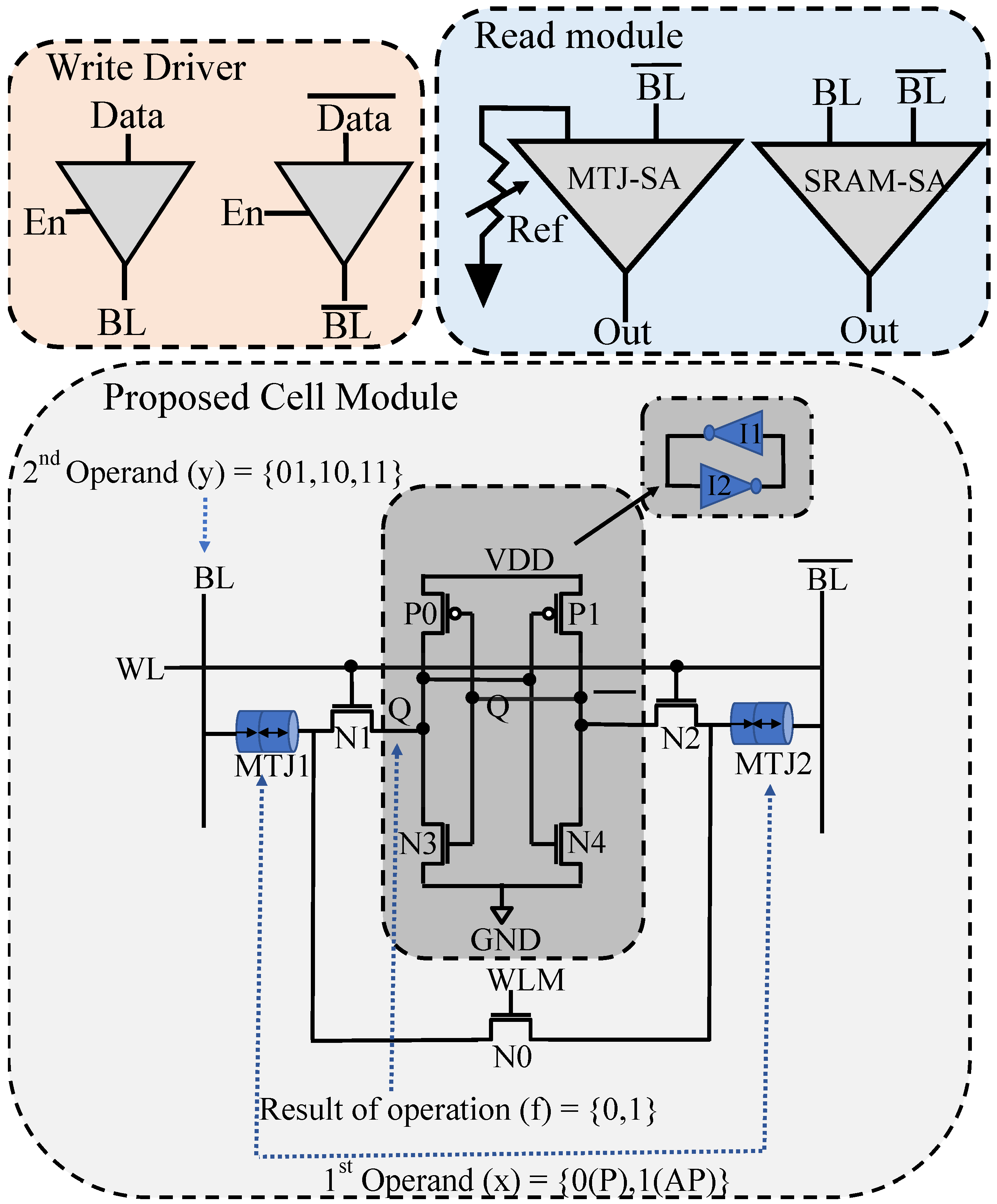
In general, the proposed cell consists of MTJs and a 6T-SRAM cell, as shown in Figure 3. The main idea of the proposed CiM is to use MTJs to prolong the SRAM write operation. The actual impact of the MTJs on the SRAM write depends on the state of the MTJs. Figure 3 presents the block diagram of the needed modules in our proposed design. As can be seen, our cell consists of a 6T-SRAM as its core. The two MTJs, MTJ1 and MTJ2, are added between this core and bitline (BL) and the complementary bitline ( BL ¯ ) , respectively. It has an additional transistor N0, which allows a current path from the BL through the two MTJs to BL ¯ , bypassing the SRAM cell. This allows one to read and write the MTJs without interfering with the SRAM content.
Overall, the cell can store two bits of information. One bit is stored in the pair of MTJs. The other one is stored in the SRAM cell. We use two differently timed SRAM write operations as a basic concept of performing CiM:
  • The long SRAM write is timed in a way that it is independent of the MTJ states. We will denote this operation as the MTJ independent write (MIW) operation.
  • The short SRAM write is timed in a way that allows for a successful write operation to the SRAM cell in case the MTJs are in the low-resistance P state. However, the write operation fails if the MTJs are in the high-resistance AP state. This short write operation is therefore dependent on the MTJ state and will be denoted as the MTJ dependent write (MDW) operation.
The truth table of the stored value in Q, depending on the MTJ states, BL, and the current state of Q, is given in Table 2 for MIW and MDW. The core of our proposed CiM-A operations is based on these two different SRAM write operations. Equations (1) and (2) represent the dependence of Q on the MIW and MDW operation parameters:
M I W : Q n e w = f ( B L )
M D W : Q n e w = f ( B L , M T J , Q o l d )
We can see that the result of the MIW operation is only dependent on the BL voltage, whereas the result of the MDW operation is also dependent on the current SRAM state Q and the MTJ state.
In order to write in the proposed cell, the write driver is used to generate the different write currents needed for the different SRAM and MTJ write operations. Two different sense schemes are used to read the SRAM value and MTJ states separately. For the CiM operations, we take advantage of the MIW and MDW SRAM operations. To perform CiM operations, we define the operands based on the value written in the MTJs in advance as well as the values that are written into the SRAM part. Writing in the SRAM cell is highly dependent on the value stored in the MTJs. Therefore, this dependability of SRAM write operations on MTJs produces the basic idea to perform the CiM operation. The CiM operation is performed by defining the proper writing sequence to the MTJs and the SRAM. In the end, the result of the operation can only be obtained by reading the content of the SRAM cell.

3.2. Circuit-Level Hybrid Cell Design

In this subsection, we describe our proposed design at the circuit level. Figure 3 gives the full schematic of our proposed cell design. The cell is interfaced via BL and BL ¯ with the control signals word line (WL) and word line MTJ (WLM). The circuit includes two back-to-back inverters (I1 and I2) to store the data and two access transistors N1 and N2. MTJ1 and MTJ2 are connected between the access transistors and the BL and BL ¯ wires. The free layer of MTJ1 is connected to the BL, whereas the reference layer of MTJ2 is connected to BL ¯ . MTJ1 and MTJ2 are connected via the write transistor N0. The role of this transistor is to make the cell able to behave as a 2M1T STT-MRAM cell. With the help of transistor N0, the MTJ can be read and written without destroying the content of the SRAM cell. As in regular SRAM, the nodes Q and Q ¯ hold the SRAM content and its complementary value. The wiring of the MTJ read/write path ensures that both MTJs are always written to the same state. Therefore, both MTJs are always either in the P state or both in the AP state.

3.2.1. CiM Operation Principle

The proposed cell performs its logic operation by writing in the SRAM cell part and the MTJs. As shown in Figure 3, two MTJs are added between the SRAM cell and the BL and BL ¯ . These two MTJs prolong the SRAM write operation. This allows us to implement the two SRAM write operations, MDW and MIW, as described at the beginning of the section. Here, we demonstrate how a few selected bitwise logic operations can be implemented. Each logic operation is defined as in Equation (3):
v = f ( x , y ) f X O R , O R , I M P
where x and y are operands of the in-memory operation and v is the result obtained by performing the logic operation.
As indicated in Equation (3), to perform a supported in-memory operation in our cell, the first operand x defines the value stored in the MTJs, and the second operand y is encoded in two consecutive SRAM write operations to the cell. After the second SRAM write operation, the result of the CiM operation is present in the SRAM part of the cell.
Figure 3 shows how these two operands are defined in our proposed cell. For the first operand, a “0” is defined with both MTJs in the P state, whereas a “1” is defined with both MTJs in the AP state. The invariant of both MTJs being in the same state all the time is enforced by the write operation. The second operand is encoded in two bits which are written to the SRAM in two consecutive operations. The first SRAM write is performed using the MIW operation to set the first bit of the encoded second operand to the SRAM. After that, the second bit of the encoded operand is stored with the MDW operation. The result in the SRAM cell is therefore dependent on the initially stored MTJ value, the previously written SRAM content of the MIW, and the operand of the MDW operation.
To put the concept of MIW versus MDW in a more vivid picture, consider Figure 4 as an example. We define the second operand as 01 (dotted signal in Figure 4a), so the first SRAM operation is writing “0” (MIW), and the second SRAM operation is using MDW to write “1”. The first enabled period of WL (the blue signal in Figure 4a) is long, so there is enough time to write in the cell under both possible MTJ states P and AP. Therefore, a “0” is present in the cell after WL is disabled the first time. The second enabled period of WL is shorter, so the state of the MTJs affects the SRAM write operation. When the state of the MTJs is AP (red signal in Figure 4b), it is not possible to write into the cell, so the previous content of the cell remains, which is “1”. In case both MTJs are in the P state (blue signal in Figure 4b), the write operation is successful, and the content of the cell becomes “1”.
We can easily see that the correct WL-enabled period plays a crucial role in performing MDW and MIW operations. With a long WL-enabled period, the state of the MTJs has no impact on the SRAM writing operation, and it is therefore not possible to perform the CiM operation. In order to use the P and AP states of the MTJs, this margin needs to be defined correctly. We name this margin the CiM_Margin, which enables us to perform the in-memory operation. The CiM_Margin is obtained according to Equation (4) for each operation:
C i M _ M a r g i n = D W ( A P ) D W ( P )
where D W ( A P ) and D W ( P ) are the write delays for the SRAM with MTJs in the AP and P states, respectively.
In general, using the state of the MTJs as the first operand and the MIW and MDW encoded value as the second operand provides the result of the CiM operation in the SRAM. Figure 5 shows the overall procedure to perform a CiM operation. To start the CiM sequence for the proposed cell, we write the first operand into the MTJs. Then, we define the type of operation that we want to perform. Choosing the operation decides the encoding of the second operand. Next, the first encoded bit is written with the MIW operation. Afterward, the second encoded bit is written with the MDW operation. The content of the SRAM now reflects the result of the selected CiM operation. The encoded second operand in the two write operations leads to a delay overhead. As the encoding is rather simple, only a small lookup table and minor adjustments to the controller logic are needed to perform the operations.

3.2.2. XOR CiM Operation

Table 3 presents the truth table for XOR operation and the corresponding MTJ states and encoding for the MIW and the MDW operations. In order to perform the XOR operation, the first operand is represented by the state of the MTJs (either P for “0” or AP for “1”), and the second operand is encoded as (“0” → 10) or (“1” → 01). In case the first operand is “0”, both MTJs are in the P state. This allows the second SRAM write operation, the MDW, to write its content to the SRAM. By design, this is the expected result of the operation. In case the first operand is “1”, both MTJs are in the AP state. This causes the MDW to fail, and therefore, the cell retains its initial values from the MIW operation, which is the expected XOR result. In summary, after the two SRAM write operations, the content of the SRAM has been set correctly to the result of the XOR operation.

3.2.3. OR CiM Operation

The next supported operation is the binary OR. We encode the first operand (“0” or “1”) as the P and AP states of the MTJs. The second operand is again encoded in two consecutive SRAM write operations. As shown in Table 3, its encoding for OR is (“0” → 10) and (“1” → 11). The reason behind this encoding is as follows. The SRAM is always initialized to “1” with the MIW operation. Then, the actual second operand of the OR operation is written to the cell with the MDW operation. If the MTJs are in the low-resistance P state, and the second operand is a “0”, then the write operation succeeds, and the SRAM cell stores a “0”. Otherwise, the cell retains its previous value of “1”. The result in the SRAM after these two write operations is therefore corresponding to the OR operation.

3.2.4. Implication CiM Operation

The third supported CiM operation of our proposed cell is the implication (IMP) function. Table 3 shows the truth table for the IMP operation and the corresponding operand encoding. As shown in the table, the first operand (“0” or “1”) is again encoded as the P and AP states of the MTJs, and the second operand is encoded in two consecutive SRAM write operations. Their encoding for IMP is (“0” → 01) and (“1” → 11). This encoding performs an MIW write operation with `0” or “1” values, depending on the input. Then, a second MDW write operation with the value of “1” is performed on the SRAM cell. As can be seen, the proposed cell can perform various types of operations.

3.3. Realization of CiM-P with the Proposed Design

In some applications, particularly multiply and accumulate (MAC) in deep learning applications, it is required to perform logic operations on the content of multiple inputs and obtain aggregated results. In such cases, CiM-P implementations are desirable. Furthermore, the ability to perform CiM-P with the presented CiM-A cell allows comparison with previous CiM-P designs. Hence, bitwise operations are also performed with the proposed cell at both the cell array and periphery part. In Section 5, we evaluate the effectiveness of the proposed CiM-A cell to be used in a CiM-P sensing scheme.
To add CiM-P capabilities, an asymmetric differential SA with skewed transistors is used [2]. The sensing process with an asymmetric differential SA is very similar to the read operation in conventional SRAM. The difference is that multiple cells are needed for selection as operands to perform bitwise logic operations. Similar to conventional memory, the logic operations are performed by pre-charging the BL and BL ¯ . Then, the corresponding WLs are enabled. Depending on the values stored in the bit cell, one of the BL or BL ¯ values is discharged. This difference on the BL and BL ¯ is sensed by the asymmetric differential SA. Figure 6 presents the selected cells in two rows of the memory along with the structure of the asymmetric differential SA.
To be more specific, consider that two values are stored in cell 1 and cell 2. First, The BL and BL ¯ are pre-charged to VDD. Then, the two corresponding WLs (WL1 and WL2) are activated simultaneously. If “00” (11) values are stored in cell1 and cell2, then the BL ( BL ¯ ) discharges to 0 while BL ¯ (BL) remains in the pre-charged state. For cases of “01” (10), both the BL and BL ¯ discharge at the same time. The differential SA generates the corresponding outputs. The results and their complements of logical operations are generated at the asymmetrical differential SA (OUT and OUT ¯ ). Transistors N BL and N BL ¯ in the asymmetric differential SA are skewed differently to make NAND (AND) and NOR (OR) possible. For the AND (NAND) operation, the transistor N BL needs to be sized larger than N BL ¯ . However, the transistor N BL ¯ is larger than N BL in the case of OR (NOR). The XOR operation is performed by using a NOR gate to merge the AND and OR outputs together, as proposed in [2]. To conclude, the proposed scheme uses a conventional SRAM style of CiM as opposed to the current sum style of scouting logic. It is not required to write in the STT-MRAM cells two times for the operands, thereby saving energy and delay overhead. Hence, the proposed scheme saves read and write energy as well as operation delay.

3.4. Conventional Memory Operations

Each SRAM and STT-MRAM part of the proposed cell can work as conventional memory. Hence, we are able to perform read and write operations. In the following, the normal memory operations of the proposed cell are described.

3.4.1. Conventional SRAM Operation

To perform the SRAM read, we use an SA which is connected to the BLs. The overall SRAM interfacing is performed exactly as in unmodified SRAM architectures. During the entire SRAM read and write operations, WLM is inactive. The MIW operation is used to ensure the storage of the new data in the SRAM part.

3.4.2. Conventional STT-MRAM

One of the considerable features of the proposed cell is the ability to read and write the STT-MRAM content independently of the SRAM content. The stored value of the SRAM part is not changed by any MTJ read or write operation. This is accomplished with the help of the transistors N1 and N2 as shown in Figure 3. These transistors create a separate path between the MTJs and the SRAM. This path can be used to read and write the MTJs. In order to read the state of the MTJs, we disconnect the SRAM cell from the BL and BL ¯ by disabling WL. However, we enable WLM to access MTJ1 and MTJ2. Since the states of these two MTJs are always the same (either P or AP), the sense margin of the read operation is improved compared with the regular 1T-1MTJ STT-MRAM cell.
We pull BL toward the ground and use a current SA to compare the current flow of a small read current through the cell to a reference current created by using a reference resistor. The resistor is sized so that it can be used to distinguish both MTJs in the P state from both MTJs in the AP state. The result of this comparison is the value of the MTJs’ content. To change the state of the MTJs, WL is disabled, and WLM is activated. Then, the high (low) voltage level on the BL and the low (high) voltage level on BL ¯ is driven to write AP to P (P to AP). In order to change the state of the MTJs, the write current needs to be greater than the critical write current. Note that the SRAM content is preserved during the MTJ writing operation due to its separate write current path.

4. Experimental Results and Evaluation

In this section, detailed circuit-level and array-level analyses are performed. First, the simulation set-up for the experiments is described. Then, the results related to the different CiM operations are presented. Finally, our proposed memory cell is compared with the previous CiM and memory designs at both the circuit and array levels.

4.1. Simulation Set-Up

Cadence Spectre was used for the circuit-level simulations. We used the 22 nm FinFet library from GlobalFoundries. There are various types of MTJ models in [46,47,48,49], which can be used for our proposed design. The proposed design needs to be adjusted accordingly based on the MTJ parameters and characteristics in each model. In this paper, we use an MTJ model as described in [46]. All simulations were performed using the same framework and technology node to be comparable. However, our concept was not limited to this single technology node. For the corner analysis, we considered all typical FinFET corners for fast- and slow-switching nFET and pFET devices (FF, SS, FS, and SF) and MTJ corners with ± 3 σ variation for the TMR, resistance-area product (RA), and the switching current. The details of the design parameters and the simulation are shown in Table 4. We considered 256 cells per BL in all evaluated RAM architectures. For the array-level evaluation, NVSim [50] was used to gather the delay, area, and energy consumption. To handle large intermediate results, the data were distributed evenly among the sub-arrays to minimize the interconnections among different sub-arrays and banks in the case of a huge volume of data. In addition, we distributed the data over the sub-array in a way where there was enough space for storing the results of the computation in the same sub-array.

4.2. CiM Operation Waveform Results

4.2.1. Operand-Encoding Signals for CiM Operations

Figure 7 shows the waveforms of the different possibilities of signal Q for performing XOR and OR operations with the proposed cell. These signals were obtained by defining the proper encoding operands for each logical operation based on the SRAM write operation and MTJ states as discussed in Section 3.2. The proper WL timing parameter was used to calculate the results of the operation inside the SRAM part.

4.2.2. Robustness of CiM Operations under Variations

Here, the functionality and robustness of the CiM operations are investigated under different process corners. The C i M _ M a r g i n needs to be large enough to ensure the proper execution of the CiM operation. Therefore, the C i M _ M a r g i n for the proposed circuit is studied under different corners to guarantee the correctness of the cell functionality.
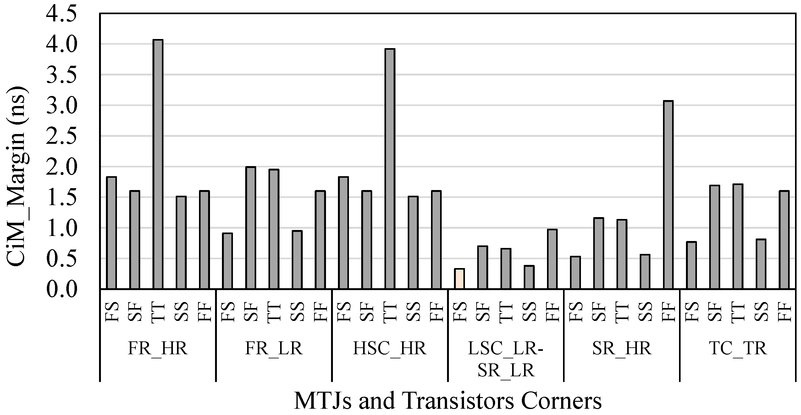
We simulated all combinations of the respective corners for both the FinFET and MTJ components to find the worst-case C i M _ M a r g i n , which affects the needed resolution of the word 0line signal. Figure 8 shows the result of the C i M _ M a r g i n for logical operations under various corners. According to Figure 8, the lowest C i M _ M a r g i n of around 276 ps can be observed in the slow pFET/slow nFET (SS) corner in combination with the low switching current corner (LSC-LR-SR-LR).
It is possible to improve C i M _ M a r g i n through several methods, which leads to reliable CiM bitwise logical operations. One way to accomplish this is to change the input signal voltage to the cell. We swept the BLs and WL voltages from 0.6 V to 0.9 V and calculated the C i M _ M a r g i n . By doing so, we reached the robustness of the C i M _ M a r g i n at 0.6 V and 0.8 V on the BLs and WL, respectively. This method increased the C i M _ M a r g i n by up to 590 ps. Another evaluated approach is to consider a higher TMR. Because the C i M _ M a r g i n is related to the difference between the states of the MTJs, increasing the TMR directly raises the C i M _ M a r g i n .

4.2.3. Impact of Temperature on the C i M _ M a r g i n

The temperature can adversely affect the functionality of the proposed design. Hence, we measured the C i M _ M a r g i n of the cell at different temperatures (10 C, 27 C, 60 C, and 85 C). Figure 9 demonstrates the C i M _ M a r g i n for logical operations in the cell. The black line is the C i M _ M a r g i n for the nominal TMR, while the two other lines present the C i M _ M a r g i n for MTJs at the higher TMR. We evaluated a TMR of up to 2.2 based on the work presented in [51].
According to this figure, first, the C i M _ M a r g i n decreased by increasing the temperature. Second, the C i M _ M a r g i n became larger for a higher TMR over the entire temperature range. In conclusion, the robustness of the CiM operation decreased by increasing the temperature, and increasing the TMR could compensate for the impact of the temperature.

4.3. Figures of Merits

As our proposed design can work as an SRAM or STT-MRAM cell, we compared its delay, energy, power, and area against a conventional 6T-SRAM and STT-MRAM (1T-1MTJ) cell and array. The evaluations also included the delay and energy for the CiM. We used peripheral circuits such as SA and write-drivers to calculate the merits at the circuit level. The cell-level analyses for memory operations as well as CiM operations are shown in Table 5, Table 6 and Table 7. As shown in Table 5, the read delay of the cell in SRAM mode was roughly the same compared with the conventional SRAM, but the write delay became around 2.78 times higher because of the presence of the MTJs. Table 6 compares the proposed cell with the conventional STT-MRAM. The write delay in the STT-MRAM part of the proposed cell was 2.22 times higher than conventional STT-MRAM, because the write operation had to change the magnetic state of two MTJs instead of only one in the conventional 1T-1MTJ memory cell. The size of the access transistor in the STT-MRAM was the same as that of the transistor connecting MTJs together in the proposed cell. However, due to the capability of storing two bits per cell, the effective per-bit area of the proposed cell was twice the size of the conventional memories. Compared with conventional SRAM and conventional STT-MRAM, the proposed cell had two more MTJs and 5Transistor+1MTJs, respectively.
For a reasonable analysis of the proposed cell compared with conventional SRAM and STT-MRAM, we present the array-level simulation results in Table 8. The parameters were calculated at the circuit level and then passed to NVSim to evaluate the cell designs in a complete RAM architecture. We considered 8 MB of memory with a 64-byte data width for both SRAM and STT-MRAM, as well as the proposed cell.
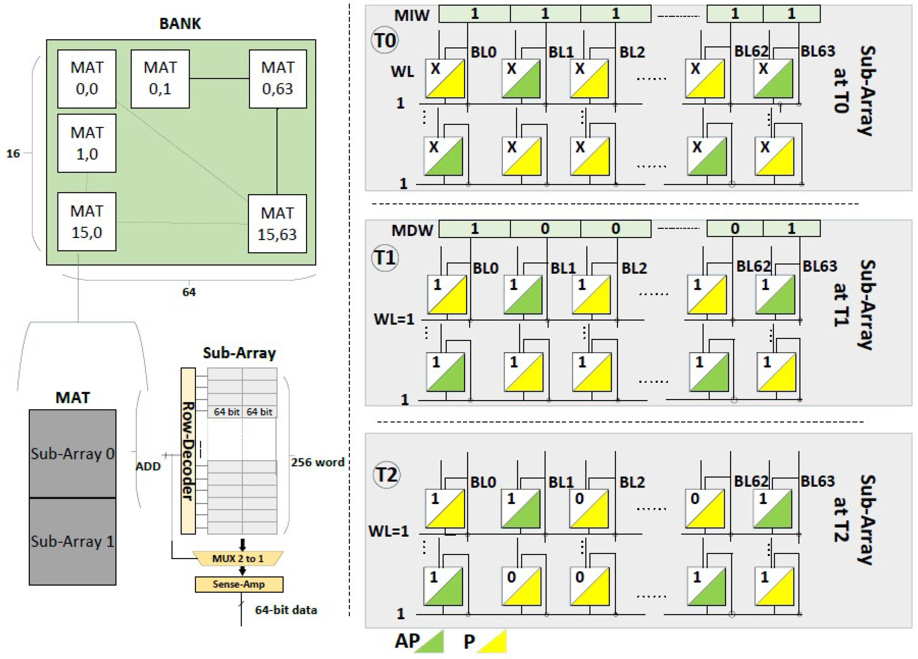
Similar to other memories, our memory design was also organized in a hierarchical structure. As shown in Figure 10, each chip was divided into banks. Each bank includes multiple sub-arrays, which were two-dimensional. To come up with such a structure, we used NVsim to map the proposed CiM-A cell to the whole memory array organization.
Figure 10 shows the detailed memory organization that was used for the array-level simulation. The read/write latencies, energy, power, and area for conventional SRAM, STT-MRAM, and the proposed cell extracted from NVSim are presented in Table 8. As expected, the ability to perform fast CiM operations directly in the memory was paid for with area, energy, and latency.
It can be seen in Table 8 that the delay and energy of a single CiM operation were well below the respective sum of multiple conventional read and write operations that would be needed to replace the CiM operation. In addition, the result of the operation is also provided in the cell. For a complete picture, Table 8 also shows the conventional memory read and write operations.

5. Analysis and Comparison to the State of the Art

In this section, several real-world applications and benchmarks are investigated to evaluate the efficiency of the proposed CiM design at the system level. Many real data-intensive applications highly depend on bitwise logic operations such as XOR, OR, and AND [7]. Table 9 presents the datasets used in this paper. To compute potential applications, we used the access latencies and energies of conventional memories (SRAM and STT-MRAM) as well as the proposed design presented in Table 7 and Table 8. We also compared the proposed design in terms of delay and energy consumption with previous existing CiM designs such as XSRAM [2] and scouting logic [16] with both the CiM-A and CiM-P parts of our designs.
For simulating scouting logic, we used a pre-charge SA. We changed the reference side of the pre-charge SA to implement various types of logical operations. SRAM-based CiM (XSRAM) was considered the same as the architecture presented in [2]. We used the asymmetric differential SA in SRAM-CiM. For previous CiM designs, first, we simulated the circuit-level approach to obtain the figures of merit, and then we obtained the array-level values to be used in the application comparison with the proposed method.
To obtain the energy and delay for each application, first, we calculated the number and type of operations in the specific application. Then, the number of required operations was multiplied by the corresponding values from the array level results for all necessary operations. To consider the complete RAM architecture for the logic operations, we used NVsim [50] to calculate the efficiency of the application in terms of energy and delay. By providing cell-level results to NVSIM, the array-level delay and energy results for the store and load operations in the memory could be obtained. Furthermore, we could use this for CiM operations based on our circuit simulation results. All evaluated applications consisted of large vector operations.
The procedure of mapping vectors to our memory organization for all applications is shown in Figure 10. First, the extracted values for the load, store, and CiM operations were used to calculate the logic operation for a single bit. Then, this value was multiplied by the vector size as well as the number of the specific operations in the applications. For the final result, all operations were summed up.
From the reliability point of view, we considered all possible conventional corners of transistors and MTJs using Cadence Spectre to confirm the proposed cell worked reliably in all situations. We used the average of all corner values for our application evaluation for a more realistic simulation. Each application is described in more detail in the following subsections.

5.1. Database Query

The first evaluated scenario was a data query application. To analyze the efficiency of the proposed CiM cell, we evaluated our design on bitmap index-based databases [52] as a widely used application, which is highly dependent on binary operations.
Bitmap-based indices were adapted by key players of the industry and found their way into many real-world applications [7]. To evaluate our approach, we used the workload of a real-life example from [53]. A database with a specific number of users (m) was given. Each user had several features (e.g. “gender” or “visited on day X”). These features were represented by bitmap-based indices. We performed the following two queries: “Number of unique users visited in the past n weeks?” and “How many male users visited each of the past n weeks?” This led to 6 n bitwise OR, 2 n 1 bitwise AND, and n + 1 bitcount operations [7]. The m-bit rows of the database were split up into m / 64 data words to be processed by the processor unit’s ALU, which can process 64 bits per read operation. However, the proposed cell could be performed on 256 bits in parallel, as it only depends on the memory organization. To perform these queries on a dataset, we assumed the access latencies and energies of conventional memories (SRAM and STT-MRAM) presented in Table 8 on a processor unit with a clock frequency of 1 GHz. Different database sizes (m) and numbers of weeks (n) were evaluated. For calculations invoking the processor unit, we calculated all overhead based on the data transfer from and to the memory without considering other resources.
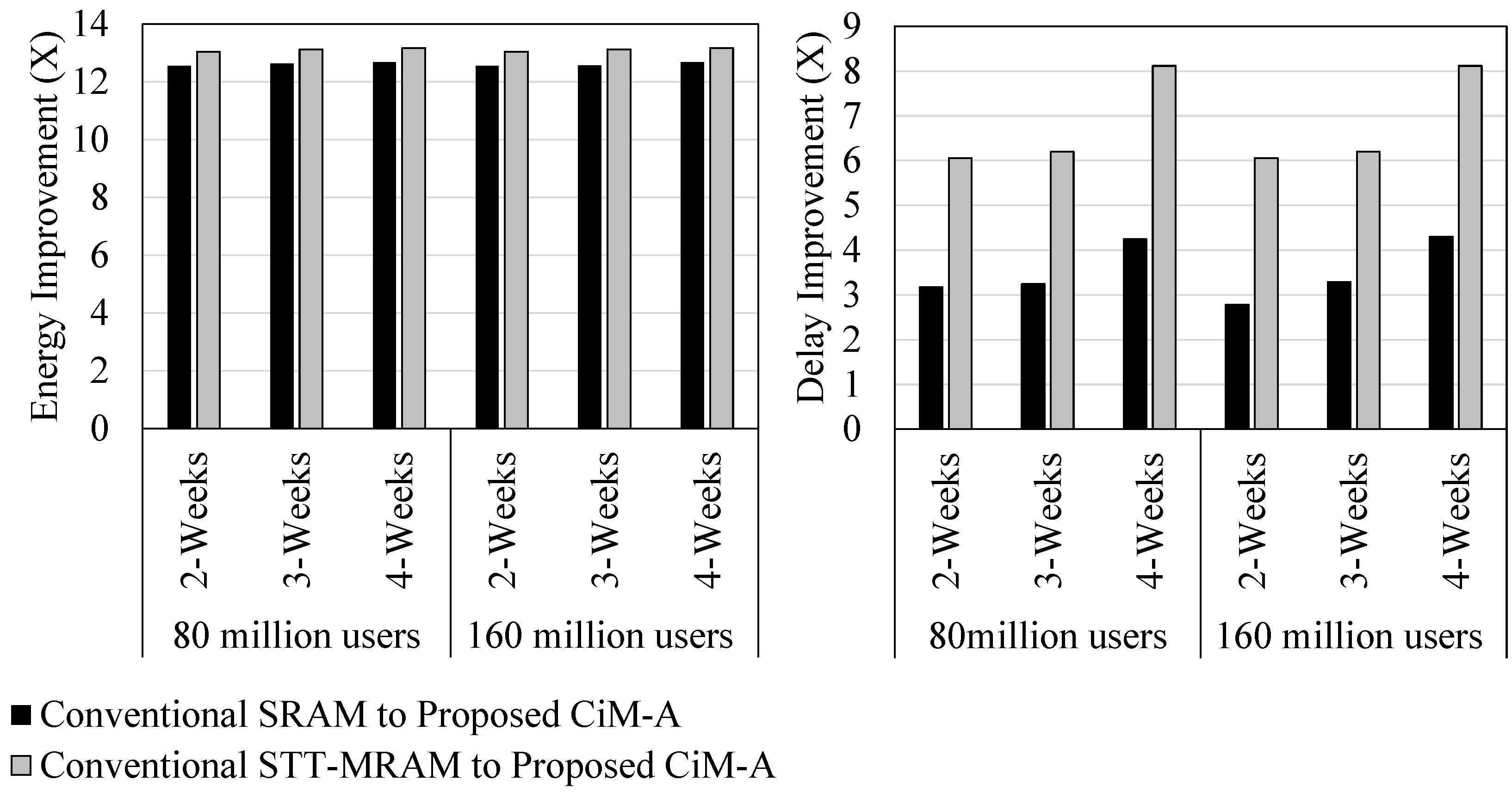
Figure 11 shows the results of the delay and energy improvement for data query application on a CPU-based (non-CiM) architecture in the proposed CiM-A. To perform this task with the proposed CiM-A architecture, the 2 n 1 AND operations had to be replaced by a sequence of inversions (which could be achieved by performing an in-memory XOR) and CiM OR operations.
According to Figure 11, the presented approach was able to speed up the execution of the workload significantly (up to four times compared with the SRAM baseline and up to eight times compared with the STT-MRAM baseline). In addition, energy improvements of 12 and 13 times compared with SRAM and STT-MRAM were achieved, respectively.
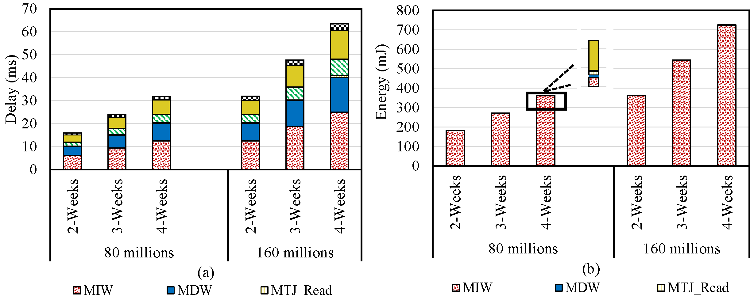
Furthermore, Figure 12 presents the comparative analysis of delay and energy consumption among various existing CiM designs. According to the evaluation, the delay and energy consumption of the proposed CiM-A were less than those of other CiMs in all evaluated workloads. To observe the proportion of each operation in CiM-A in more detail, CiM-A was divided into operations such as MIW, MDW, SRAM read, and MTJ write, as shown in Figure 13. As we can see in Figure 13, the MIW operations dominated the delay and energy consumption of the complete CiM operation. Since other operations except MIW were not visible in the energy consumption of the proposed CiM-A, we magnified some parts of the chart to highlight the other operations. Since all bitmap queries include various bitwise operations, it was expected that we would find similar performance and energy efficiency for any applications using bitmap indices.

5.2. Bit Vector Set

Another bitwise application scenario is the bit vector set. There are many algorithms using the set data structure [7,54]. For example, it is used for graph mining. One way of implementing a set with a fixed size is to use a bit vector [55]. In the bit vector function, each bit represents a corresponding element. It is possible to perform bitwise operations among bit vectors for multiple operations such as union, intersections, and difference.
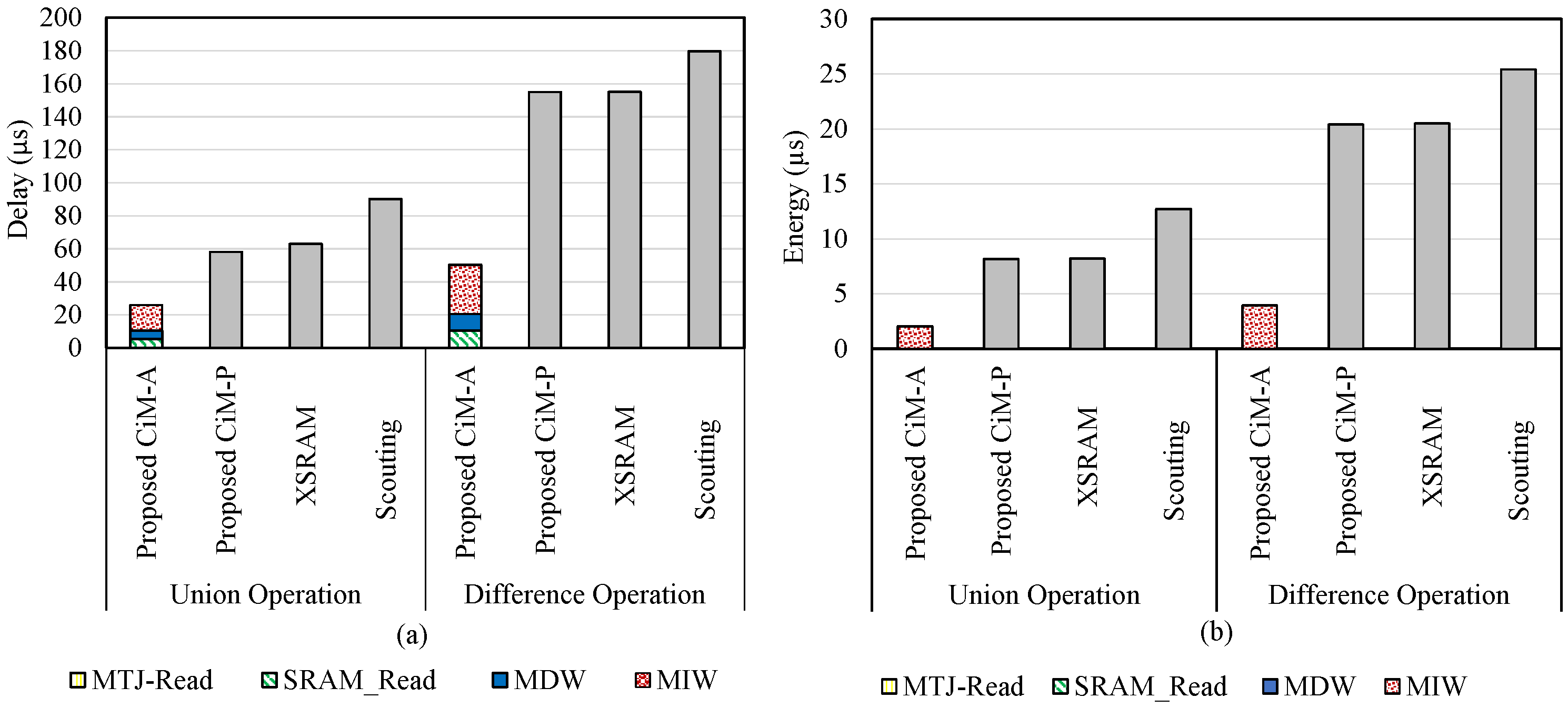
Table 10 presents the energy and delay of the union and the different operations for various memory designs using CiM-A. For this evaluation, we assumed a bit vector of 512K to represent the set. The union and difference operations were performed on 15 input sets. As is shown, CiM-A could improve the delay and energy by 2.24 and 4 times compared with XSRAM for union operation, respectively. These numbers for STT-based scouting logic design could reach 3.48 and 6.23 times the value in terms of delay and energy, respectively. Figure 14 presents the delay and energy for XSRAM, STT-based scouting, and the proposed CiM-A and CiM-P. The delay and energy for CiM-A consist of MIW, MDW, MTJ_read, and SRAM_Read operations. Figure 14 depicts the breakdown of delay and energy consumption for the proposed CiM-A architecture. As shown in these figures, most of the delay and energy consumption could be traced back to the MIW. For the energy evaluation, the MIW operation was the only visible contributor to the total energy consumption due to its large overall contribution compared with the other operations. Figure 14 presents the absolute values for the delay and energy. Typically, more complex operations result in a larger overhead in terms of delay and energy. The difference operation is more complex, as it includes more logic operations than union operations. Therefore, performing the difference operation requires more energy and a larger delay compared with the union operation, as shown in Figure 14. However, both operations profited from the presented design.

5.3. Pure Bitwise Operation

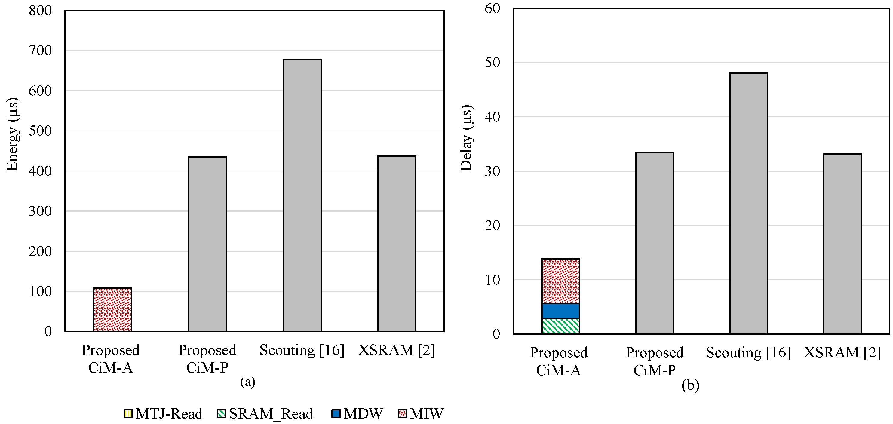
We also evaluated the proposed design on the pure bitwise operation to measure its efficiency [56]. Pure bitwise operations are part of many real-world applications such as graphs and data mining [57,58]. In addition, pure bitwise operations are used in bio-informatics to implement genetic algorithms [59]. Table 11 presents the delay and the energy of the pure XOR operation among 32 rows for XSRAM, the scouting CiM design, and conventional memory (STT-MRAM and SRAM) relative to the proposed CiM-A architecture. Performing XOR with the proposed CiM-A could improve the delay and energy consumption compared with other CiM architectures and conventional memories. Figure 15 presents the values of this delay and energy consumption for various CiM designs.
Moreover, the breakdown of the needed operations for the proposed CiM-A is shown. As shown in Figure 15, the proposed CiM-A performed XOR operations with less delay and energy consumption, with MIW being the dominant contributor in the CiM-A operation in terms of both delay and energy.

6. Conclusions

The computation-in-memory paradigm seems to be a promising approach to tackling the memory wall and high energy consumption issues. Emerging non-volatile memory types provides an efficient boolean logic implementation inside the memory. In this paper, we proposed a hybrid SRAM/STT-MRAM cell that performs logic operations within the memory array and saves the result of a CiM operation directly within the cell. A comprehensive evaluation of the cell and the array level were presented to validate the functionality of the proposed design. The proposed cell can significantly reduce delay and energy consumption compared with other STT-MRAM- and SRAM-based CiM-P implementations. We further showed the reliability and correctness of the design under process and temperature variations. The simulation results show that the proposed CiM architecture could achieve up to 8 times greater speeds and 13 times less energy consumed compared with conventional memory types for typical data-intensive applications with negligible overhead.

Author Contributions

Conceptualization, A.J., C.M., M.T.; Methodology, A.J., C.M.; Implementation, A.J., C.M.; Writing—original draft preparation, A.J., C.M.; Writing—review and editing, M.T.; visualization, A.J., C.M.; supervision, M.T.; funding acquisition, M.T. All authors have read and agreed to the published version of the manuscript.

Funding

This research was funded partly by a grant from German Research Foundation under grant number TA782/43-1.

Conflicts of Interest

The authors declare no conflict of interest.

References

  1. Seshadri, V.; Hsieh, K.; Boroum, A.; Lee, D.; Kozuch, M.A.; Mutlu, O.; Gibbons, P.B.; Mowry, T.C. Fast Bulk Bitwise AND and OR in DRAM. IEEE Comput. Archit. Lett. 2015, 14, 127–131. [Google Scholar] [CrossRef]
  2. Agrawal, A.; Jaiswal, A.; Lee, C.; Roy, K. X-SRAM: Enabling In-Memory Boolean Computations in CMOS Static Random Access Memories. IEEE Trans. Circuits Syst. I Regul. Pap. 2018, 65, 4219–4232. [Google Scholar] [CrossRef] [Green Version]
  3. Nair, S.M.; Bishnoi, R.; Vijayan, A.; Tahoori, M.B. Dynamic Faults based Hardware Trojan Design in STT-MRAM. In Proceedings of the 2020 Design, Automation Test in Europe Conference Exhibition (DATE), Grenoble, France, 9–13 March 2020; pp. 933–938. [Google Scholar] [CrossRef]
  4. Sebastian, A.; Le Gallo, M.; Khaddam-Aljameh, R.; Eleftheriou, E. Memory devices and applications for in-memory computing. Nat. Nanotechnol. 2020, 15, 529–544. [Google Scholar] [CrossRef] [PubMed]
  5. Li, C.; Hu, M.; Li, Y.; Jiang, H.; Ge, N.; Montgomery, E.; Zhang, J.; Song, W.; Dávila, N.; Graves, C.E.; et al. Analogue signal and image processing with large memristor crossbars. Nat. Electron. 2018, 1, 52–59. [Google Scholar] [CrossRef]
  6. Khalifa, M.; Ben-Hur, R.; Ronen, R.; Leitersdorf, O.; Yavits, L.; Kvatinsky, S. FiltPIM: In-Memory Filter for DNA Sequencing. In Proceedings of the 2021 28th IEEE International Conference on Electronics, Circuits, and Systems (ICECS), Dubai, United Arab Emirates, 28 November–1 December 2021; pp. 1–4. [Google Scholar]
  7. Seshadri, V.; Lee, D.; Mullins, T.; Hassan, H.; Boroumand, A.; Kim, J.; Kozuch, M.A.; Mutlu, O.; Gibbons, P.B.; Mowry, T.C. Ambit: In-Memory Accelerator for Bulk Bitwise Operations Using Commodity DRAM Technology. In Proceedings of the IEEE/ACM International Symposium on Microarchitecture (MICRO), Cambridge, MA, USA, 14–18 October 2017. [Google Scholar]
  8. Karunaratne, G.; Le Gallo, M.; Cherubini, G.; Benini, L.; Rahimi, A.; Sebastian, A. In-memory hyperdimensional computing. Nat. Electron. 2020, 3, 327–337. [Google Scholar] [CrossRef]
  9. Hamdioui, S.; Du Nguyen, H.A.; Taouil, M.; Sebastian, A.; Le Gallo, M.; Pande, S.; Schaafsma, S.; Catthoor, F.; Das, S.; Redondo, F.G.; et al. Applications of computation-in-memory architectures based on memristive devices. In Proceedings of the 2019 Design, Automation & Test in Europe Conference & Exhibition (DATE), Florence, Italy, 25–29 March 2019; pp. 486–491. [Google Scholar]
  10. Jain, S.; Ranjan, A.; Roy, K.; Raghunathan, A. Computing in memory with spin-transfer torque magnetic RAM. IEEE Trans. Very Large Scale Integr. (VLSI) Syst. 2017, 26, 470–483. [Google Scholar] [CrossRef]
  11. Edelstein, D.; Rizzolo, M.; Sil, D.; Dutta, A.; DeBrosse, J.; Wordeman, M.; Arceo, A.; Chu, I.C.; Demarest, J.; Edwards, E.R.J.; et al. A 14 nm Embedded STT-MRAM CMOS Technology. In Proceedings of the 2020 IEEE International Electron Devices Meeting (IEDM), San Francisco, CA, USA, 12–18 December 2020; pp. 11.5.1–11.5.4. [Google Scholar] [CrossRef]
  12. Guo, Q.; Guo, X.; Patel, R.; Ipek, E.; Friedman, E.G. Ac-dimm: Associative computing with stt-mram. In Proceedings of the International Symposium on Computer Architecture, Washington, DC, USA, 23–26 October 2013. [Google Scholar]
  13. Wright, C.D.; Hosseini, P.; Diosdado, J.A.V. Beyond von-Neumann computing with nanoscale phase-change memory devices. Adv. Funct. Mater. 2013, 23, 2248–2254. [Google Scholar] [CrossRef] [Green Version]
  14. Sebastian, A.; Le Gallo, M.; Eleftheriou, E. Computational phase-change memory: Beyond von Neumann computing. J. Phys. D Appl. Phys. 2019, 52, 443002. [Google Scholar] [CrossRef]
  15. Ielmini, D.; Wong, H.S.P. In-memory computing with resistive switching devices. Nat. Electron. 2018, 1, 333–343. [Google Scholar] [CrossRef] [Green Version]
  16. Xie, L.; Du Nguyen, H.A.; Yu, J.; Kaichouhi, A.; Taouil, M.; AlFailakawi, M.; Hamdioui, S. Scouting logic: A novel memristor-based logic design for resistive computing. In Proceedings of the IEEE Computer Society Annual Symposium on VLSI (ISVLSI), Bochum, Germany, 3–5 July 2017. [Google Scholar]
  17. Sayed, N.; Mao, L.; Tahoori, M.B. Dynamic behavior predictions for fast and efficient hybrid STT-MRAM caches. ACM J. Emerg. Technol. Comput. Syst. (JETC) 2021, 17, 1–21. [Google Scholar] [CrossRef]
  18. Boujamaa, E.M.; Ali, S.M.; Wandji, S.N.; Gourio, A.; Pyo, S.; Koh, G.; Song, Y.; Song, T.; Kye, J.; Vial, J.C.; et al. A 14.7 Mb/mm2 28nm FDSOI STT-MRAM with Current Starved Read Path, 52Ω/Sigma Offset Voltage Sense Amplifier and Fully Trimmable CTAT Reference. In Proceedings of the IEEE Symposium on VLSI Circuits, Kolkata, India, 4–8 January 2020. [Google Scholar] [CrossRef]
  19. Chang, T.C.; Chiu, Y.C.; Lee, C.Y.; Hung, J.M.; Chang, K.T.; Xue, C.X.; Wu, S.Y.; Kao, H.Y.; Chen, P.; Huang, H.Y.; et al. 13.4 A 22nm 1Mb 1024b-Read and Near-Memory-Computing Dual-Mode STT-MRAM Macro with 42.6GB/s Read Bandwidth for Security-Aware Mobile Devices. In Proceedings of the 2020 IEEE International Solid- State Circuits Conference—(ISSCC), San Francisco, CA, USA, 16–20 February 2020; pp. 224–226. [Google Scholar] [CrossRef]
  20. Nguyen, H.A.D.; Yu, J.; Lebdeh, M.A.; Taouil, M.; Hamdioui, S.; Catthoor, F. A classification of memory-centric computing. ACM J. Emerg. Technol. Comput. Syst. (JETC) 2020, 16, 1–26. [Google Scholar] [CrossRef] [Green Version]
  21. Kvatinsky, S.; Belousov, D.; Liman, S.; Satat, G.; Wald, N.; Friedman, E.G.; Kolodny, A.; Weiser, U.C. MAGIC—Memristor-aided logic. IEEE Trans. Circuits Syst. II Express Briefs 2014, 61, 895–899. [Google Scholar] [CrossRef]
  22. Nair, S.M.; Bishnoi, R.; Tahoori, M.B. Mitigating Read Failures in STT-MRAM. In Proceedings of the 2020 IEEE 38th VLSI Test Symposium (VTS), San Diego, CA, USA, 5–8 April 2020; pp. 1–6. [Google Scholar] [CrossRef]
  23. Khvalkovskiy, A.; Apalkov, D.; Watts, S.; Chepulskii, R.; Beach, R.; Ong, A.; Tang, X.; Driskill-Smith, A.; Butler, W.; Visscher, P.; et al. Basic principles of STT-MRAM cell operation in memory arrays. J. Phys. D Appl. Phys. 2013, 46, 074001. [Google Scholar] [CrossRef]
  24. Mayahinia, M.; Jafari, A.; Tahoori, M.B. Voltage Tuning for Reliable Computation in Emerging Resistive Memories. In Proceedings of the 2022 IEEE VLSI Test Symposium (VTS), San Diego, CA, USA, 25–27 April 2022; pp. 1–7. [Google Scholar] [CrossRef]
  25. Yu, J.; Du Nguyen, H.A.; Xie, L.; Taouil, M.; Hamdioui, S. Memristive devices for computation-in-memory. In Proceedings of the 2018 Design, Automation & Test in Europe Conference & Exhibition (DATE), Dresden, Germany, 19–23 March 2018; pp. 1646–1651. [Google Scholar]
  26. Borghetti, J.; Snider, G.S.; Kuekes, P.J.; Yang, J.J.; Stewart, D.R.; Williams, R.S. ‘Memristive’switches enable ‘stateful’logic operations via material implication. Nature 2010, 464, 873–876. [Google Scholar] [CrossRef] [PubMed]
  27. Kvatinsky, S.; Satat, G.; Wald, N.; Friedman, E.G.; Kolodny, A.; Weiser, U.C. Memristor-based material implication (IMPLY) logic: Design principles and methodologies. IEEE Trans. Very Large Scale Integr. (VLSI) Syst. 2013, 22, 2054–2066. [Google Scholar] [CrossRef]
  28. Rohani, S.G.; TaheriNejad, N. An improved algorithm for IMPLY logic based memristive full-adder. In Proceedings of the IEEE Canadian Conference on Electrical and Computer Engineering (CCECE), Windsor, ON, Canada, 30 April–3 May 2017. [Google Scholar]
  29. Teimoory, M.; Amirsoleimani, A.; Shamsi, J.; Ahmadi, A.; Alirezaee, S.; Ahmadi, M. Optimized implementation of memristor-based full adder by material implication logic. In Proceedings of the IEEE International Conference on Electronics, Circuits and Systems (ICECS), Marseille, France, 7–10 December 2014. [Google Scholar]
  30. Hur, R.B.; Wald, N.; Talati, N.; Kvatinsky, S. SIMPLE MAGIC: Synthesis and in-memory mapping of logic execution for memristor-aided logic. In Proceedings of the IEEE/ACM International Conference on Computer-Aided Design (ICCAD), Westminster, CO, USA, 4–7 November 2017. [Google Scholar]
  31. Talati, N.; Gupta, S.; Mane, P.; Kvatinsky, S. Logic design within memristive memories using memristor-aided loGIC (MAGIC). IEEE Trans. Nanotechnol. 2016, 15, 635–650. [Google Scholar] [CrossRef]
  32. Linn, E.; Rosezin, R.; Tappertzhofen, S.; Böttger, U.; Waser, R. Beyond von Neumann—logic operations in passive crossbar arrays alongside memory operations. Nanotechnology 2012, 23, 305205. [Google Scholar] [CrossRef]
  33. Snider, G. Computing with hysteretic resistor crossbars. Appl. Phys. A 2005, 80, 1165–1172. [Google Scholar] [CrossRef]
  34. Xie, L.; Du Nguyen, H.A.; Taouil, M.; Hamdioui, S.; Bertels, K. Fast boolean logic mapped on memristor crossbar. In Proceedings of the IEEE International Conference on Computer Design (ICCD), Washington, DC, USA, 18–21 October 2015. [Google Scholar]
  35. Kang, W.; Wang, H.; Wang, Z.; Zhang, Y.; Zhao, W. In-memory processing paradigm for bitwise logic operations in STT–MRAM. IEEE Trans. Magn. 2017, 53, 1–4. [Google Scholar]
  36. Pan, Y.; Ouyang, P.; Zhao, Y.; Kang, W.; Yin, S.; Zhang, Y.; Zhao, W.; Wei, S. A multilevel cell STT-MRAM-based computing in-memory accelerator for binary convolutional neural network. IEEE Trans. Magn. 2018, 54, 1–5. [Google Scholar] [CrossRef]
  37. Guo, X.; Ipek, E.; Soyata, T. Resistive computation: Avoiding the power wall with low-leakage, STT-MRAM based computing. ACM SIGARCH Comput. Archit. News 2010, 38, 371–382. [Google Scholar] [CrossRef]
  38. Jovanović, B.; Brum, R.M.; Torres, L. Comparative analysis of MTJ/CMOS hybrid cells based on TAS and in-plane STT magnetic tunnel junctions. IEEE Trans. Magn. 2014, 51, 1–11. [Google Scholar] [CrossRef]
  39. Monga, K.; Chaturvedi, N.; Gurunarayanan, S. Design of a novel CMOS/MTJ-based multibit SRAM cell with low store energy for IoT applications. Int. J. Electron. 2020, 107, 899–914. [Google Scholar] [CrossRef]
  40. Janniekode, U.M.; Somineni, R.P.; Khalaf, O.I.; Itani, M.M.; Chinna Babu, J.; Abdulsahib, G.M. A Symmetric Novel 8T3R Non-Volatile SRAM Cell for Embedded Applications. Symmetry 2022, 14, 768. [Google Scholar] [CrossRef]
  41. Fujita, S.; Noguchi, H.; Nomura, K.; Abe, K.; Kitagawa, E.; Shimomura, N.; Ito, J. Novel nonvolatile L1/L2/L3 cache memory hierarchy using nonvolatile-SRAM with voltage-induced magnetization switching and ultra low-write-energy MTJ. IEEE Trans. Magn. 2013, 49, 4456–4459. [Google Scholar] [CrossRef]
  42. Mittal, S.; Verma, G.; Kaushik, B.; Khanday, F.A. A Survey of SRAM-Based Processing-in-Memory Techniques and Applications. Available online: https://www.researchgate.net/profile/Sparsh-Mittal-2/publication/351344022_A_Survey_of_SRAM-based_Processing-in-Memory_Techniques_and_Applications/links/60922686458515d315f760c6/A-Survey-of-SRAM-based-Processing-in-Memory-Techniques-and-Applications.pdf (accessed on 23 October 2022).
  43. Wu, P.C.; Su, J.W.; Chung, Y.L.; Hong, L.Y.; Ren, J.S.; Chang, F.C.; Wu, Y.; Chen, H.Y.; Lin, C.H.; Hsiao, H.M.; et al. A 28 nm 1 Mb Time-Domain Computing-in-Memory 6T-SRAM Macro with a 6.6 ns Latency, 1241GOPS and 37.01 TOPS/W for 8b-MAC Operations for Edge-AI Devices. In Proceedings of the 2022 IEEE International Solid-State Circuits Conference (ISSCC), San Francisco, CA, USA, 20–24 February 2022; Volume 65, pp. 1–3. [Google Scholar]
  44. Su, J.W.; Chou, Y.C.; Liu, R.; Liu, T.W.; Lu, P.J.; Wu, P.C.; Chung, Y.L.; Hung, L.Y.; Ren, J.S.; Pan, T.; et al. 16.3 A 28nm 384kb 6T-SRAM Computation-in-Memory Macro with 8b Precision for AI Edge Chips. In Proceedings of the 2021 IEEE International Solid- State Circuits Conference (ISSCC), San Francisco, CA, USA, 13–22 February 2021; Volume 64, pp. 250–252. [Google Scholar] [CrossRef]
  45. Guo, R.; Liu, Y.; Zheng, S.; Wu, S.Y.; Ouyang, P.; Khwa, W.S.; Chen, X.; Chen, J.J.; Li, X.; Liu, L.; et al. A 5.1 pJ/Neuron 127.3us/Inference RNN-based Speech Recognition Processor using 16 Computing-in-Memory SRAM Macros in 65 nm CMOS. In Proceedings of the 2019 Symposium on VLSI Circuits, Kyoto, Japan, 9–14 June 2019; pp. C120–C121. [Google Scholar] [CrossRef]
  46. Mejdoubi, A.; Prenat, G.; Dieny, B. A compact model of precessional spin-transfer switching for MTJ with a perpendicular polarizer. In Proceedings of the International Conference on Microelectronics Proceedings, Algiers, Algeria, 16–20 December 2012. [Google Scholar]
  47. De Rose, R.; d’Aquino, M.; Finocchio, G.; Crupi, F.; Carpentieri, M.; Lanuzza, M. Compact modeling of perpendicular STT-MTJs with double reference layers. IEEE Trans. Nanotechnol. 2019, 18, 1063–1070. [Google Scholar] [CrossRef]
  48. Cuchet, L.; Rodmacq, B.; Auffret, S.; Sousa, R.C.; Prejbeanu, I.L.; Dieny, B. Perpendicular magnetic tunnel junctions with double barrier and single or synthetic antiferromagnetic storage layer. J. Appl. Phys. 2015, 117, 233901. [Google Scholar] [CrossRef]
  49. Wang, H.; Kang, W.; Zhang, Y.; Zhao, W. Modeling and evaluation of sub-10-nm shape perpendicular magnetic anisotropy magnetic tunnel junctions. IEEE Trans. Electron Dev. 2018, 65, 5537–5544. [Google Scholar] [CrossRef]
  50. Dong, X.; Xu, C.; Xie, Y.; Jouppi, N.P. Nvsim: A circuit-level performance, energy, and area model for emerging nonvolatile memory. IEEE Trans. Comput. Aided Des. Integr. Circuits Syst. 2012, 31, 994–1007. [Google Scholar] [CrossRef]
  51. Song, Y.; Lee, J.; Han, S.; Shin, H.; Lee, K.; Suh, K.; Jeong, D.; Koh, G.; Oh, S.; Park, J.; et al. Demonstration of highly manufacturable STT-MRAM embedded in 28nm logic. In Proceedings of the 2018 IEEE International Electron Devices Meeting (IEDM), San Francisco, CA, USA, 1–5 December 2018; pp. 18–22. [Google Scholar]
  52. Chan, C.Y.; Ioannidis, Y.E. Bitmap index design and evaluation. In Proceedings of the ACM SIGMOD International Conference on Management of Data, San Jose, CA, USA, 1–4 June 1998. [Google Scholar]
  53. Denir, D.; AbdelRahman, I.; He, L.; Gao, Y. Audience Insights Query Engine. Available online: https://www.facebook.com/business/news/audience-insights (accessed on 23 October 2022).
  54. Besta, M.; Kanakagiri, R.; Kwasniewski, G.; Ausavarungnirun, R.; Beránek, J.; Kanellopoulos, K.; Janda, K.; Vonarburg-Shmaria, Z.; Gianinazzi, L.; Stefan, I.; et al. SISA: Set-Centric Instruction Set Architecture for Graph Mining on Processing-in-Memory Systems. arXiv 2021, arXiv:2104.07582. [Google Scholar]
  55. Std::set, std::bitset. Available online: https://en.cppreference.com/w/cpp/utility/bitset (accessed on 23 October 2022).
  56. Li, S.; Xu, C.; Zou, Q.; Zhao, J.; Lu, Y.; Xie, Y. Pinatubo: A processing-in-memory architecture for bulk bitwise operations in emerging non-volatile memories. In Proceedings of the Design Automation Conference (DAC), Austin, TX, USA, 5–9 June 2016. [Google Scholar]
  57. Beamer, S.; Asanovic, K.; Patterson, D. Direction-optimizing breadth-first search. In Proceedings of the SC’12: Proceedings of the International Conference on High Performance Computing, Networking, Storage and Analysis, Washington, DC, USA, 10–16 November 2012; pp. 1–10. [Google Scholar]
  58. Bogdanov, D.; Niitsoo, M.; Toft, T.; Willemson, J. High-performance secure multi-party computation for data mining applications. Int. J. Inf. Secur. 2012, 11, 403–418. [Google Scholar] [CrossRef]
  59. Pedemonte, M.; Alba, E.; Luna, F. Bitwise operations for GPU implementation of genetic algorithms. In Proceedings of the 13th Annual Conference Companion on Genetic and Evolutionary Computation, Dublin, Ireland, 12–16 July 2011; pp. 439–446. [Google Scholar]
Figure 1. STT-MRAM device: (a) MTJ as a storing device for values of 0 and 1 and (b) STT-MRAM cell.
Jlpea 12 00063 g001
Figure 2. The impact of temperature on resistance distributions of P and AP for STT-MRAM at nominal voltage and at 27 C and 85 C.
Jlpea 12 00063 g002
Figure 3. Schematic of a spintronic 2M/7T computation-in-memory cell, where two MTJs always at the same resistance states are used to store the data bit, and the SRAM part is used to store another data bit to have CiM. Read and write peripheral modules are shown to read and write the data stored in both the SRAM and MTJ parts.
Jlpea 12 00063 g003
Figure 4. MDW transitions depend on MTJ states. The short WL pulse allows Q to change from “0” to “1” only if the MTJ is in the P state. (a) Control signals to perform the operation. (b) Inner node Q of SRAM part for AP and P MTJ states.
Jlpea 12 00063 g004
Figure 5. The overall procedure to implement logical operations with proposed CiM design.
Jlpea 12 00063 g005
Figure 6. Schematic of the proposed cell for performing CiM-P logic, including the asymmetric differential SA with skewed transistor operations.
Jlpea 12 00063 g006
Figure 7. XOR and OR operation signal waveforms. (a) Signal Q for XOR with different SRAM writing and MTJ states. (b) Signal Q for OR with different SRAM writing and MTJ states.
Jlpea 12 00063 g007
Figure 8. Sense margin of the CiM operations for different process corners of transistors (TT, FF, SF, FS, and SS) and MTJs (TC_TR, SR_HR, LSC_LR-SR_LR, HSC_HR, FR_LR, and FR_HR) with transistor corners (T: typical, F: fast, and S: slow) and MTJ corners (TC_TR: typical current, typical resistance; SR_HR: slow read, high resistance; LSC_LR-SR_LR: low switching current, low resistance; HSC_HR: high switching current, high resistance; FR_LR: fast read, low resistance; and FR_HR: fast read, high resistance).
Jlpea 12 00063 g008
Figure 9. The impact of temperature on the C i M _ M a r g i n for various TMR values in the proposed cell.
Jlpea 12 00063 g009
Figure 10. Memory array organizations considered in this paper for simulation results at circuit and array level, with number of banks and MATs and sub-array size. In addition, the procedure of mapping vector and logic operation performance is shown. One of the operands is stored as an MTJ state, which is shown by a green triangle (AP state) and yellow triangle (P state). Another operand is based on the SRAM encoded into MIW and MDW presented in two time steps (T1 and T2), and the result of the operation is produced in the cell based on the state of the MTJ and SRAM in the third time step (T3). Note: SRAM state at the first time step (T0) is not important, denoted by X.
Jlpea 12 00063 g010
Figure 11. Quantification of the energy and delay for the proposed CiM-A design compared with conventional SRAM and STT-MRAM for the bitmap index-based database application [7].
Jlpea 12 00063 g011
Figure 12. Delay and energy consumption comparison between various CiM designs for bitmap index database queries.
Jlpea 12 00063 g012
Figure 13. Breakdown of operations for delay and energy consumption of the proposed CiM-A architecture. The MIW in the proposed CiM-A is the dominant part compared with other operations in terms of both delay and energy.
Jlpea 12 00063 g013
Figure 14. Delay and energy of union and difference operations for various CiM designs are shown in (a) and (b), respectively. The proposed CiM-A is broken down into individual operations such as MTJ_Read, SRAM_Read, MDW, and MIW.
Jlpea 12 00063 g014
Figure 15. Energy and delay for pure XOR among different CiM designs. Breakdown of the proposed CiM-A into used operations (MTJ_Read, SRAM_Read, MDW, and MIW).
Jlpea 12 00063 g015
Table 1. Read decision failure (RDF) for STT-MRAM and ReRAM memories at 25 C and 85 C. (CiM-X in scouting logic shows the X numbers of operands in a column, which can be activated together simultaneously.)
MemoriesSTT-MRAMReRAM
Temperature25 C85 C25 C85 C
CiM-24.24 × 5 1.59 × 10 4 5.57 × 10 10 2.77 × 10 8
CiM-43.27 × 10 3 4.49 × 10 3 2.77 × 10 8 1.31 × 10 10
CiM-80.22050.221073.74 × 10 5 1.90 × 10 6
Table 2. Cell state transitions for MIW and MDW operations.
MTJBL Q old Q new
MIWMDW
P0000
P0100
P1011
P1111
AP0000
AP0101
AP1010
AP1111
Table 3. The truth table based on encoding operands as used for different logical operations.
Different Logical Operations
XOR OperationOR OperationIMP Operation
xyf (x,y)xyf (x,y)xyf (x,y)
0 (P)0 (10)00 (P)0 (10)00 (P)0 (01)1
0 (P)1 (01)10 (P)1 (11)10 (P)1 (11)1
1 (AP)0 (10)11 (AP)0 (10)11 (AP)0 (01)0
1 (AP)1 (01)01 (AP)1 (11)11 (AP)1 (11)1
Table 4. Technology parameters for the simulation set-up.
ParametersValue
SRAM, STT-MRAM and proposed Memory Size8 MB
Technology Node22 nm
Supply Voltage and Temperature0.8 V and 27 C
Radius of MTJ20 nm
MTJ Barrier MaterialMgO
Nominal Tunneling Magneto-Resistance Ratio150%
Resistance-Area Product in MTJ7.5 Ω μ m 2
Free/Oxide Layer Thickness1.31/1.48 nm
`P”/“AP” Resistance6 k Ω / 15 k Ω
Table 5. Circuit-level results for conventional SRAM compared with the proposed cell design. The technology parameters are set according to Table 4 for the nominal corner.
ParametersConventional
SRAM
Proposed
Cell
Compared with
SRAM
Read Delay1.79 ns1.89 ns1.01 ×
Read Energy5.30 fJ7.67 fJ1.44 ×
Write Delay
with MTJ
-3.79 ns2.78 ×
Write Delay
without MTJ
1.36 ns-
Write Energy
with MTJ
-104.90 fJ1.19 ×
Write Energy
without MTJ
16.00 fJ-
Numbers of Transistors
or MTJs
6 Transistors6 Transistors
+2 MTJs
+2 MTJs
Table 6. Circuit-level results for conventional STT-MRAM compared with the proposed cell design. The technology parameters are set according to Table 4 for the nominal corner.
ParametersConventional
STT-MRAM
Proposed
Cell
Compared with
STT-MRAM
Read Delay458 ps687 ps1.50 ×
Read Energy2.80 fJ3.40 fJ1.21 ×
Write Delay5.43 ns12.1 ns2.22 ×
Write Energy190 fJ400 fJ2.10 ×
Numbers of Transistors
or MTJs
1 Transistor
+1 MTJ
6 Transistors
+2 MTJs
+2 MTJs
Table 7. Circuit-level results for the proposed CiM. The technology parameters are set according to Table 4 for the nominal corner.
ParametersMDW DelayMDW EnergyMIW DelayMIW Energy
Proposed
CiM1.71 ns87.75 fJ1.82 ns104.90 fJ
Table 8. Array-level results for conventional SRAM, STT-MRAM, and the proposed CiM design for 8 MB memory with a 64-byte data width and a subarray organization of 256 rows × 128 columns.
ParametersSRAMSTT-MRAMProposed Cell
Operating as
Overhead to
SRAMSTT-MRAMSRAMSTT-MRAM
Area5.67 mm 2 4.33 mm 2 9.63 mm 2 1.69×2.22×
Read Latency2.55 ns4.18 ns2.57 ns4.23 ns1.00×1.01×
Write Latency2.58 ns7.28 ns5.01 ns13.95 ns1.94×1.91×
Read Energy65.43 pJ67.25 pJ65.59 pJ74.49 pJ1.00×1.10×
Write Energy65.05 pJ68.96 pJ66.20 pJ82.42 pJ1.01×1.19×
CiM Latency--6.72 ns--
CiM Energy--66.21 pJ--
Table 9. Datasets and benchmarks.
ApplicationsDescriptionImplementation Detail
DatabaseBitmap-based datasetQuery to track users’ characteristics and activities
SetImplementing set with N-bit bit vectorPerform Union and difference operations on 15-input sets
VectorPure XOR operation2 17 vectors, 32 rows of XOR operations
Table 10. Delay and energy comparison of the proposed CiM-A for union and difference set operations normalized to our proposed CiM-A.
ParametersConventional
SRAM
Conventional
STT-MRAM
Scouting Logic
 [16]
XSRAM [2]Proposed
CiM-P
Proposed
CiM-A
Union
Operation
Delay (X)4.797.413.482.242.401
Energy (X)11.8113.736.234.004.001
Difference
Operation
Delay (X)4.916.613.563.003.001
Energy (X)10.1711.566.455.215.171
Table 11. Delay and energy comparison related to the proposed CiM-A for pure XOR operation, normalized to our proposed CiM-A.
ParametersConventional SRAMSTT-MRAMScouting LogicXSRAMProposed CiM-PProposed CiM-A
Delay (X)4.778.843.462.382.401
Energy (X)11.8112.756.024.024.001
Publisher’s Note: MDPI stays neutral with regard to jurisdictional claims in published maps and institutional affiliations.