Abstract
This paper is an extended version of a previously reported conference paper regarding a low-power design for NAND Flash. As the number of bits per NAND Flash die increases with cost scaling, the IO data path speed increases to minimize the page access time with a scaled CMOS in IOs. The power supply for IO buffers, namely, VDDQ, decreases from 3 V to 1.2 V, accordingly. In this paper, the way in which a reduction in VDDQ can contribute to power reduction in the BL path is discussed and validated. Conventionally, a BL voltage of about 0.5 V has been supplied from a supply voltage source (VDD) of 3 V. The BL path power can be reduced by a factor of VDDQ to VDD when the BL voltage is supplied by VDDQ. To maintain a sense margin at the sense amplifiers, the supply source for BLs is switched from VDDQ to VDD before sensing. As a result, power reduction and an equivalent sense margin can be realized at the same time. The overhead of implementing this operation is an increase in the BL access time of about 2% for switching the power supply from VDDQ to VDD and an increase in the die size of about 0.01% for adding the switching circuit, both of which are not significant in comparison to the significant power reduction in the BL path power of the NAND die of about 60%. The BL path is then designed in 180 nm CMOS to validate the design. When the cost for powering the SSD becomes quite significant, especially for data centers, an additional lower voltage supply, such as 0.8 V, dedicated to BL charging for read and program verifying operations may be the best option for future applications.
1. Introduction
As of 2020, data centers accounted for 1% of the worldwide electricity use [1]. As cloud services such as artificial intelligence, autonomous vehicles, and distributed manufacturing systems have been expanding, more data centers are required. Their energy use has been predicted to increase by a factor of three or four within the next decade. As a result, many researchers have been focusing on power reduction without affecting computing performance.
Figure 1 compares power breakdowns for data centers in the following areas [2,3,4]: (1) servers and storage systems, (2) cooling and humidification systems, (3) power conditioning equipment, (4) networking equipment, and (5) lighting/physical security. A server’s power strongly depends on the workload. The cooling power depends on the ambient weather conditions around the data center facility in question. These three data sources show that servers and cooling consume about 80% of data centers’ total power needs. Figure 2 shows the breakdown of “servers” into CPU, DRAM, and storage. Storage includes hard disk drives (HDDs) and NAND Flash-based solid-state drives (SSDs). NAND Flash memory is a nonvolatile semiconductor memory. As bit density increases, SSDs whose storage components are NAND Flash memory drives have been replacing hard disk drives in data centers as well as personal computers because of their lower power usage and faster latency.
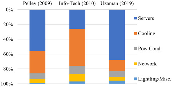
Figure 1.
Power breakdowns for data centers shown in three different sources [2,3,4].
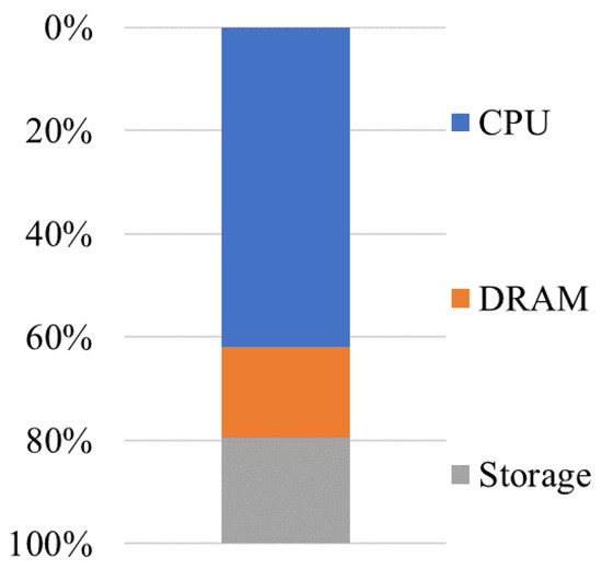
Figure 2.
Breakdown in “Servers” [4].
Distributed temperature control units control the local temperature surrounding CPUs running with different workloads [5]. As a result, the total power for servers and cooling can be minimized. The energy-efficient distribution of power converters is also important in reducing the total power requirements of data centers [6]. Shuffled topologies spread secondary power feeds over the power grid, which allows for a single power unit failure. Power routing schedules workload dynamically. The network consumes much less power than the servers and the cooling system at full utilization. However, since servers typically operate at much lower levels of utilization, the network power cannot be ignored. If a system is 15% utilized and the servers are fully energy-proportional, the network will consume about 50% of the overall power used [7]. Thus, the network power needs to be proportional to the workload. It has been shown that a flattened butterfly topology is itself inherently more power-efficient than the other commonly proposed topology for high-performance datacenter networks [7]. Database software also affect the energy efficiency of servers. It has been shown that CPUs’ power consumption varies by as much as 60% depending on the operators for the same CPU level of utilization [8]. Thus, data centers’ energy consumption depends on each of the following aspects: individual hardware such as CPUs, memory, storage, cooling, and network; construction and control of the hardware and software; and workload and environmental temperature. Therefore, energy consumption models are important in designing energy-efficient data centers and optimizing their operations. Reference [9] surveys more than 200 models for all the hierarchical levels of the hardware. In [10], analytical models called FlashPower were developed to estimate NAND Flash memory chip energy dissipation during basic flash operations such as read, program, and erase. Each component, such as selected and unselected word lines (WLs), bit lines (BLs) for data 0 and 1, source lines, decoders, and sense amplifiers, is parameterized for each operation.
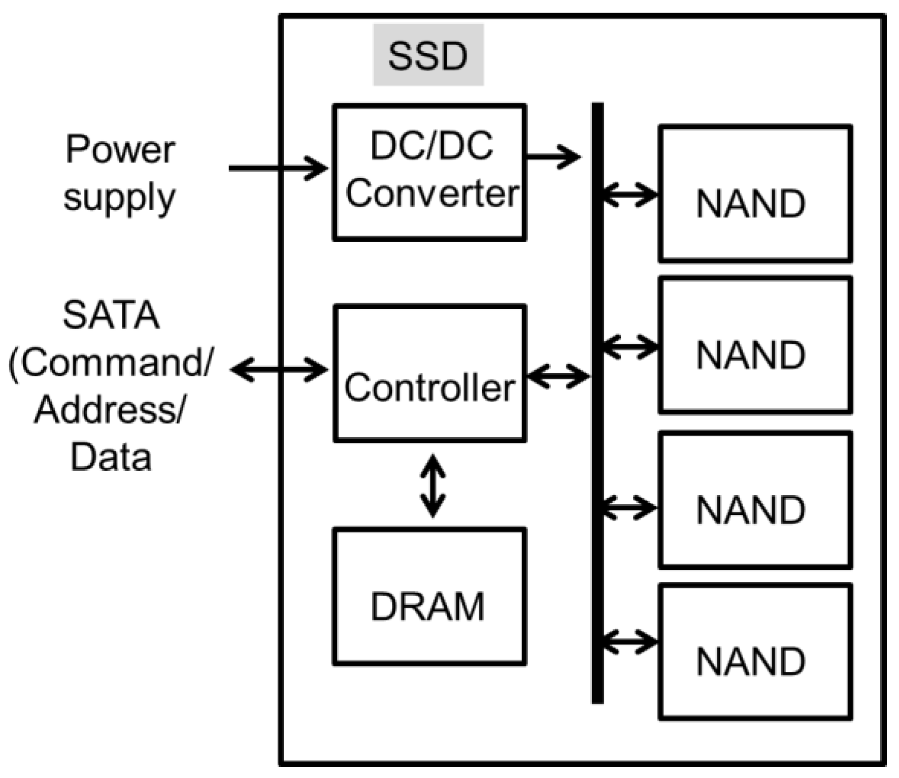
Now, let us take a look at the inside of an SSD. Figure 3 illustrates a block diagram of the internal structure of an SSD [11]. Multiple NAND Flash drives are integrated to store large volumes of data. DRAM is used as a memory buffer for multiple NAND drives. An SSD controller controls data traffic at the interface between the SATA (serial advanced technology attachment) and the NAND drives. When data are written into the SSD, the sequential written data inputs to the SSD are stored in the DRAM first and then are transferred to one or more NAND dies through a data bus inside the SSD, according to the written address. When data are read out of the SSD, the sequential data are moved from one or more NAND to the DRAM through the data bus inside the SSD first and then are transferred to the SATA. A DC/DC converter inputs power from a 3 V power source to output multiple voltages for the controller, NAND, and DRAM.

Figure 3.
Block diagram of the internal structure of an SSD.
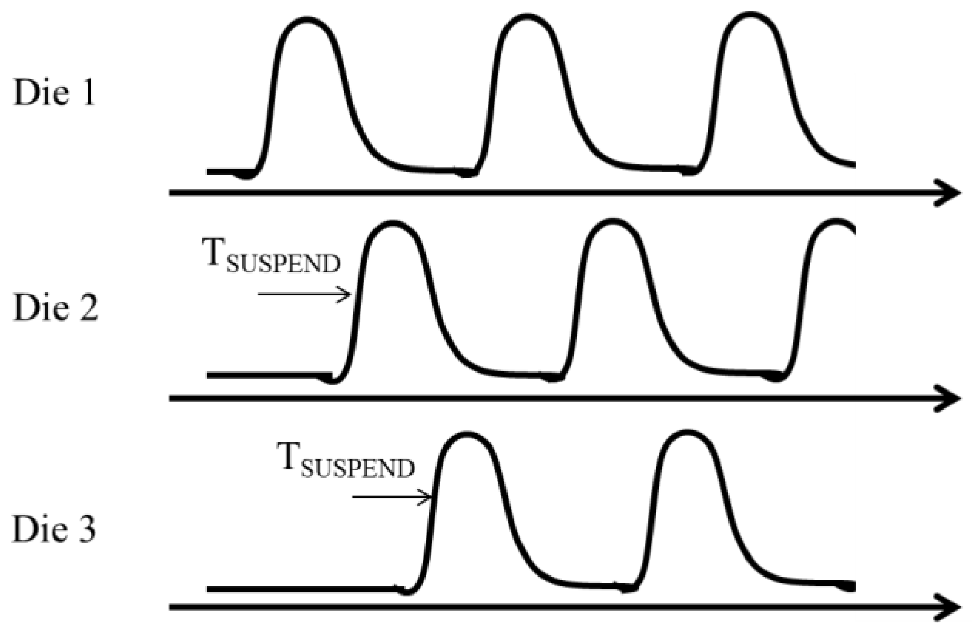
The array access time of NAND is much longer than that of DRAM by factors of 1000 for the read operation and of 10,000 for the write operation. In order to increase the band width for the read and write operations, multiple NAND dies in an SSD operate in parallel. The maximum number of NAND dies operating in parallel is determined by the peak power [12]. The peak point occurs when heavily capacitive WLs and BLs are charged up. As shown in Figure 4, the peak point can be shifted by adding a suspend time (TSUSPEND) between the NAND dies, which improves the parallelism. It is more favorable to reduce the power itself not only for parallelism but also for energy reduction in the SSDs and in the data center.

Figure 4.
IDD waveform of three drives operating in parallel.
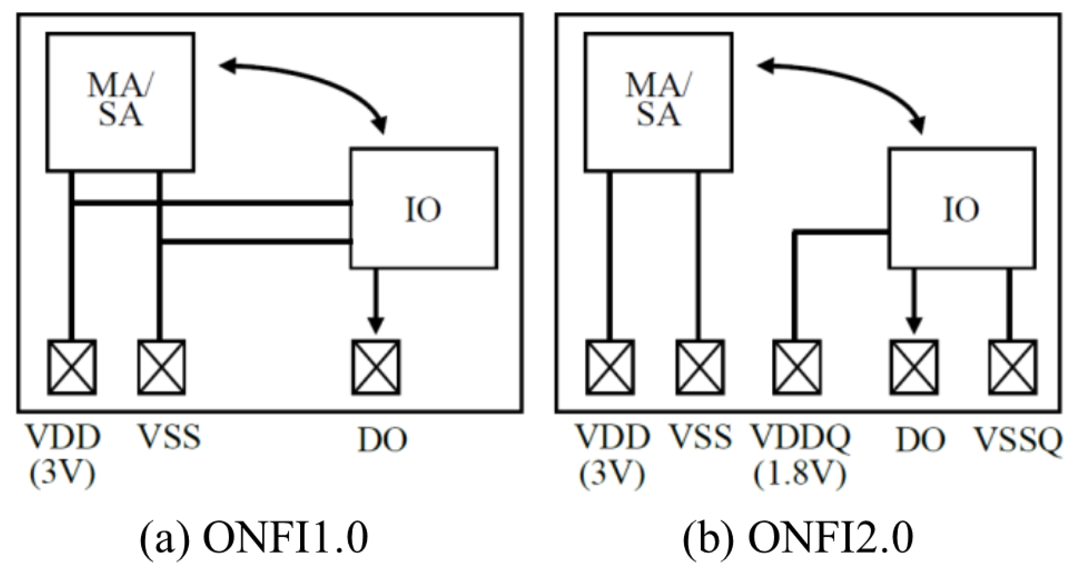
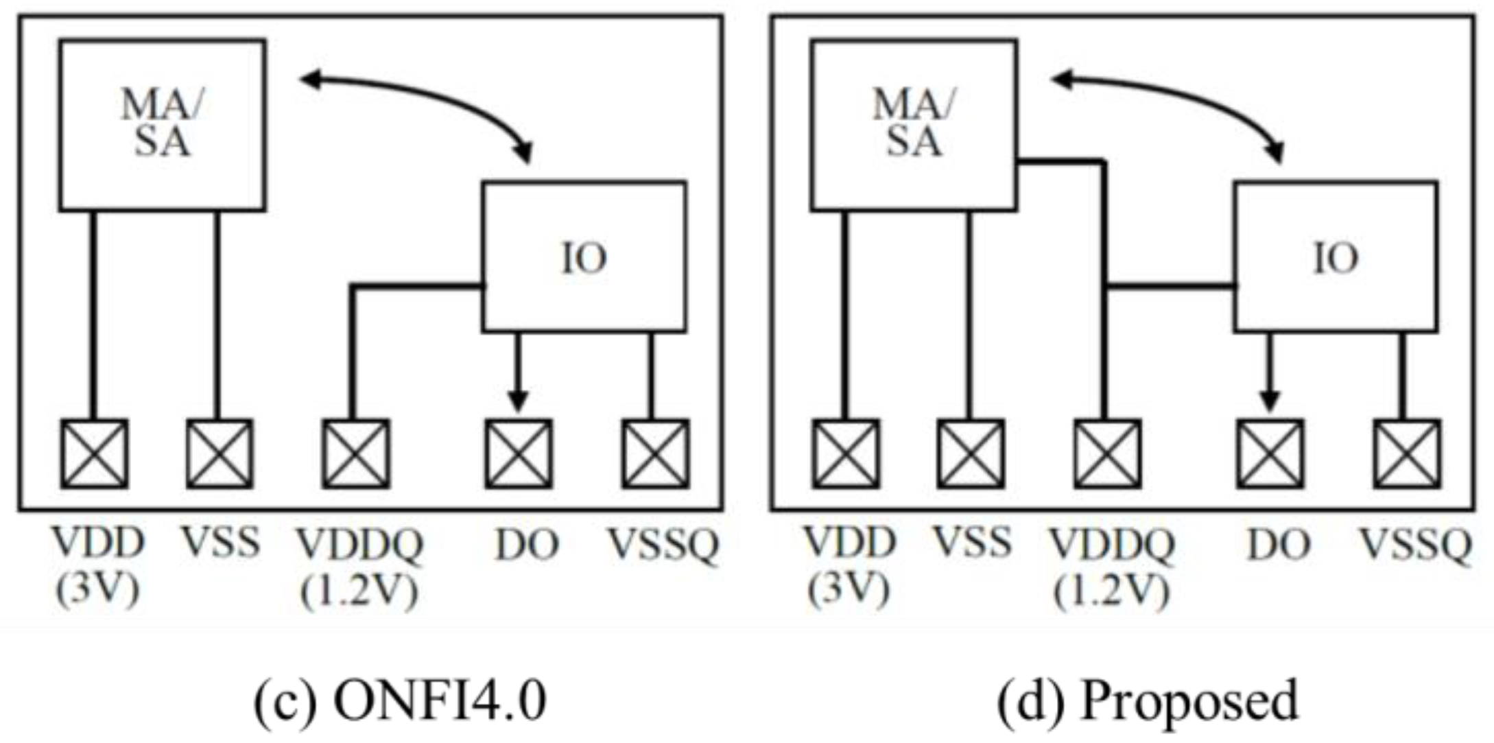
As the NAND bit density increases, page length increases from 512 B to 16 KB. Because read and program operations are carried out on a page basis, the IO speed needs to increase accordingly in order to prevent a bottleneck at the IO path in the data traffic. In order to make it easier to develop an advanced SSD controller and an advanced SSD, two groups, the Open NAND Flash Interface (ONFI) [13] and Toggle [14] working groups, have standardized the interface of NAND. Figure 5 illustrates the power distribution for a NAND dies with ONFI 1.0 (a), 2.0 (b), and 4.0 (c) and the proposed power distribution in a NAND die (d). MA, SA, and IO are the memory array, the sense amplifier, and the IO buffers, respectively. In order to increase the bandwidth of the NAND interface, IO transistors are scaled. As a result, the power supply for IO buffers, namely, VDDQ, decreases from 3 V to 1.8 V and from 1.8 V to 1.2 V. A 2.4 Gb/s IO speed has been previously achieved in a 1 Tb 3D NAND Flash [15]. The ONFI 1.0 NAND has one set of a VDD power supply and a ground VSS. IO operates at 3 V with VDD/VSS. Since the creation of ONFI 2.0 [16,17], the power/ground for IO is dedicated to VDDQ/VSSQ to allow for scaled transistors operating at a lower voltage for faster IO operation. VDD remains at 3 V even when VDDQ is lowered, because high voltages of over 20 V for program and erase operations need to be generated by charge pumps on a chip [18]. If VDD were to be scaled like VDDQ, the charge pumps would have increased circuit areas, which would affect the cost. In order to further improve IO operation frequency for increasing band widths, more scaled transistors require a lower VDDQ of 1.2 V with ONFI 4.0 [19]. As shown in Figure 5d, the proposed design [20] utilizes VDDQ not only for IO buffers but also for SA to significantly reduce the power in the BL path, as will be described in the following sections.
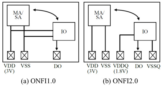
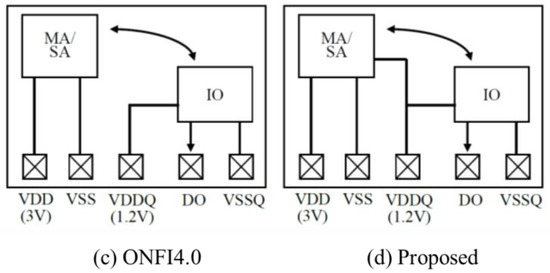
Figure 5.
Power distribution for NAND dies with ONFI 1.0 (a), 2.0 (b), and 4.0 (c). Proposed power distribution in a NAND dies (d). MA: memory array; SA: sense amplifier; and IO: IO buffers. The arrows show the data path between SA and IO.
This paper is an extended version of a previously reported conference paper [20] regarding a low-power design for NAND Flash with an existing NAND Flash interface. NAND Flash dies with this low-power design can replace existing ones without any additional cost, because there is no need to update the printed circuit boards for the SSDs and the design of the NAND controller.
This paper is organized as follows: Section 2 overviews and models two operations for BL read access: shielded-BL (SBL) [21] and all-BL (ABL) [22] read operations. Section 3 compares the circuit diagrams and read operations in the conventional and proposed circuits for the ABL read operation. Experimental results are shown in Section 4. Section 5 discusses design considerations such as scalability in BL capacitance and noise immunity.
2. BL Access for Read Operation
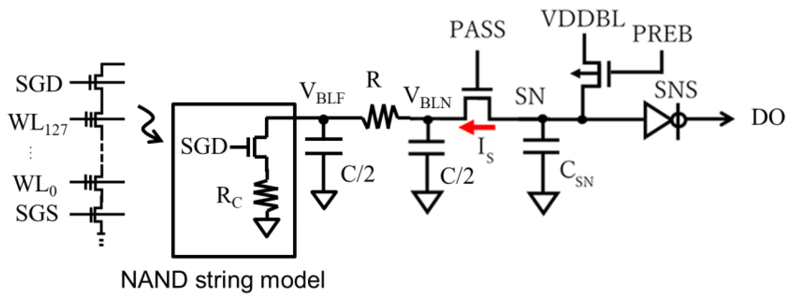
Figure 6 illustrates the BL path of NAND Flash. This section overviews and models two operations for BL read access: SBL [21] and ABL [22] read operations. A long, narrow, and tightly pitched BL has a relatively high parasitic resistance and capacitance, as depicted by R and C. Multiple cells are connected with the BL. (For simplicity, Figure 6 shows only one of them connected at the farthest node, which has the longest delay). The gates of NAND Flash cells are connected with WLs and two selected gates (SGD, SGS). A read operation is carried out as follows: Only a selected WL, e.g., WL127, goes up to a certain voltage, e.g., 1 V, while the other deselected WLs and the two selected gates go up to a higher voltage, such as 5 V, to turn on regardless of the cell’s threshold voltages. When the selected cell has a threshold voltage below 1 V, it turns on, while, if this threshold is above 1 V, it turns off.

Figure 6.
BL path of NAND Flash. The arrow indicates that a NAND string is modeled by the circuit enclosed by a rectangle.
NAND string is modeled by a switching transistor controlled by the SGD signal as a switch and a linear resistor RC for simplicity. In this paper, the cell data are related to RC as follows: the cell whose data are 0, namely, 0-cell, has a much lower current than the cell whose data are 1, namely, 1-cell, i.e., the 0-cell has a much higher RC than the 1-cell. The BL is modeled by a simple 2 π RC model. The PASS gate acts as a source follower to limit the BL voltage VBL to about 0.5 V. The lower boundary is determined by the value at which the cell current enters into a linear region where the cell current ICELL has a strong function as VBL. The BL access time increases as ICELL decreases. The higher boundary is limited by reliability. A too-high VBL increases the probability of a hot carrier injection into the gate of the cell transistors, resulting in a substantial shift in the cell’s threshold voltage. From the viewpoint of power, VBL should be as low as possible. The lower the VBL, the lower the power in the BL path. SN indicates the “storage node”. The parasitic capacitance CSN stores charges temporarily, whose amounts are translated into digital values of 1 or 0 at the DO by a clocked invertor controlled by a sensing signal SNS. The BL is charged up through the PREB transistor from VDDBL.
2.1. BL Delay Time in the Case of a Shielded-BL Read
Figure 7 shows the waveform of the BL control signals and VBL for an SBL read operation. The BL access time TBL (TSBL for SBL and TABL for ABL) is the sum of a pre-charge period TPRE and a discharge period TDIS. The BL starts charging up with PASS high and PREB low. Because SGD is forced to ground during TPRE, VBLF and VBLN go up regardless of the cell data. The discharge period starts with PASS low and SGD high. Depending on the cell data, VBLN gradually lowers by ΔVBL for 1-cell, whereas it remains the same for 0-cell. After TDIS, PASS goes up to a voltage slightly lower by ΔVPASS than that in TPRE. SN rapidly lowers for 1-BL, with ΔVBL > ΔVPASS, whereas it keeps the voltage for 0-BL as high as VDDBL. With SNS high, DO is set to present the cell data.
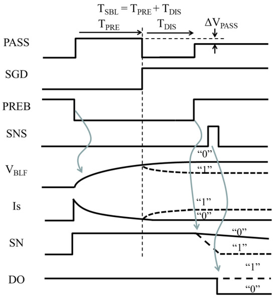
Figure 7.
Waveform for an SBL read operation. The arrows indicate signal propagation. The dash lines show the signals for “1”-date.
Next, TSBL is estimated with the simple model shown in Figure 6. Assuming VBLN, VBL at the nearest node to the sense amplifier is forced to a constant voltage of VBL_PRE with PASS high in TPRE, VBLF, and VBL. VBL at the farthest node from the sense amplifier is given by Equation (1).
In TDIS, the differential equations for VBLN and VBLF are given by (2) and (3).
Using the initial conditions of (4) and (5),
VBLN(t) is solved to be (6).
where , f1, VA, and VB are defined by (7)–(10), respectively.
ΔVBL = VBL_PRE − VBLN(TDIS) can be calculated by (6) at t = TDIS, with specific RC values for 0-cell and 1-cell.
2.2. BL Delay Time in the Case of an All-BL Read
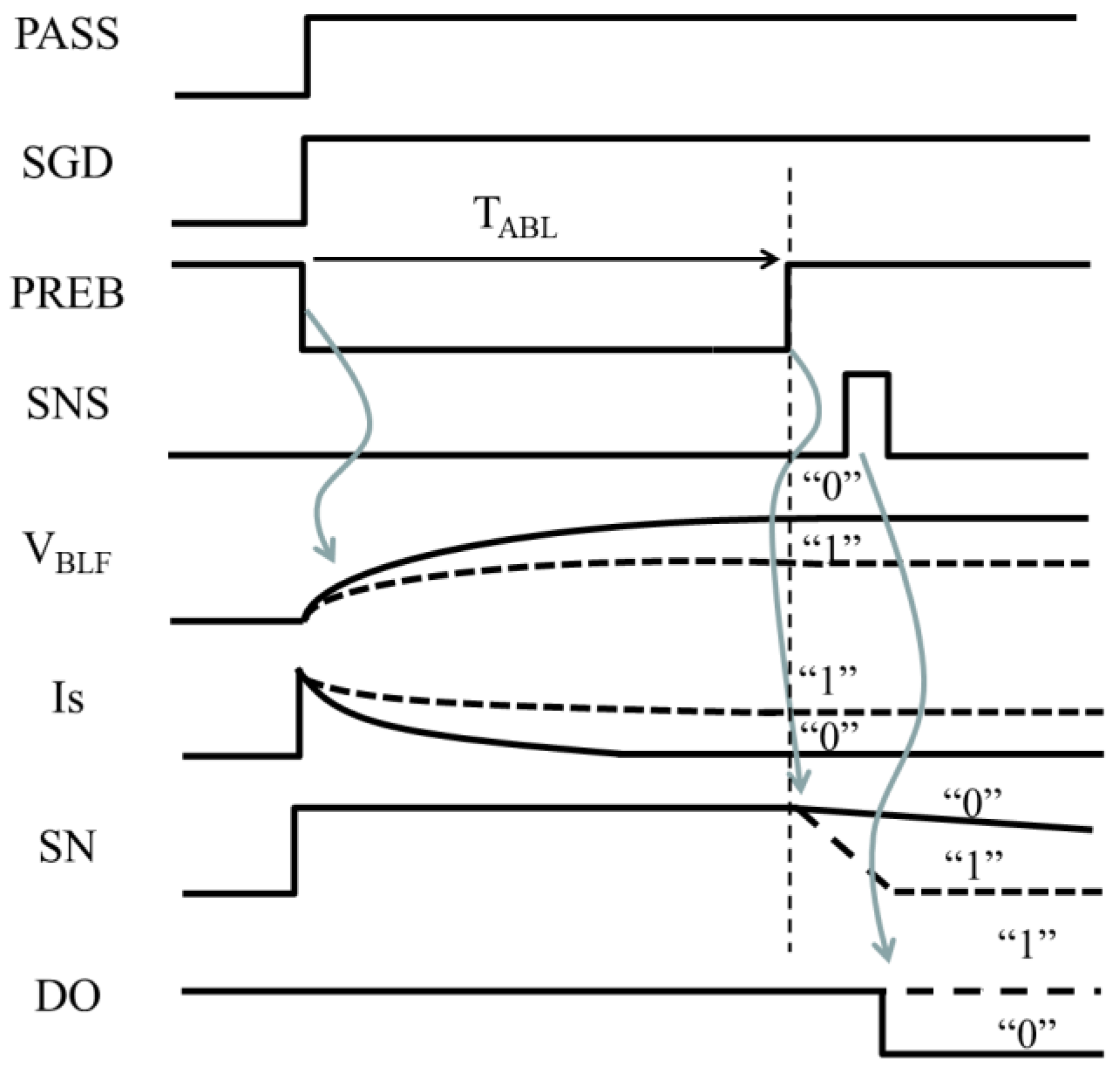
Figure 8 shows the waveform of the BL control signals and VBL for an ABL read operation. The BL starts charging up with SGD and PASS high and PREB low. The VBLF goes up depending on the cell data. The VBLF for 1-cell is lower than that for 0-cell. The sense current IS approaches the cell current. After TABL, PASS increases to discharge CSN. SN rapidly lowers for 1-BL in comparison to 0-BL. When VSN becomes low enough, SNS toggles to transfer the cell data to DO.

Figure 8.
Waveform for an ABL read operation. The arrows indicate signal propagation. The dash lines show the signals for “1”-date.
TABL is estimated as follows. VBLF is governed by (11), which is solved as (12), with the initial condition of VBLF (0) = 0.
IS can be calculated by (13).
A sense margin for ABL can be defined by %IS. Thus, TABL is a function of %IS.
2.3. Energy in the BL Path
VDDBL supplies energy (ESBL) into every BL as given by (15), regardless of data 1 or 0 in the case of SBL.
On the other hand, ABL requires more energy because VDDBL needs to supply a direct cell current in addition to the displacement current for the BL parasitic capacitance, as given by (16), where EABL is the averaged energy per BL.
2.4. Performance Comparison between SBL and ABL
TABL and EBL depend on a sensing scheme such as SBL or ABL, on technology-dependent parameters such as R and C, and on design parameters such as VBL_PRE, ΔVBL, and %IS. It is challenging to determine which sensing scheme is better than the other in terms of performance generally, but it would be good to demonstrate their comparison under a specific condition. In this sub-section, the following parameters are used as a demonstration: ; ; ; ; VDDBL = 2.0 V; = 25, 50, and 75 mV for SBL; and 70, 80, and 90% for ABL. VBL_PRE is also skewed, as shown in Table 1.

Table 1.
Condition of VBL_PRE for demonstration.
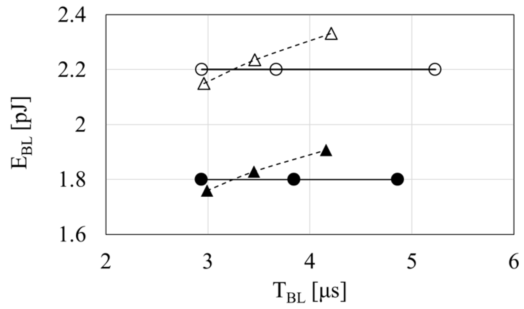
Figure 9 shows a performance comparison between SBL with = 25, 50, and 75 mV (from left to right) and ABL with 70, 80, and 90% (from left to right). Note that the condition was selected so as to have crossing points between the SBL and the ABL. More sensing margins result in a longer BL delay but do not contribute (for SBLs) or provide a minor contribution (for ABLs) to the energy for the read operation in the BL path. A finite slope of EBL(TBL) curves for the ABL comes from the cell current. The longer the TBL with more sensing margin, the greater the integration of power due to the cell current. In Section 3 and afterwards, a proposed design is based on ABLs, but its effectiveness on energy reduction is also expected with SBLs.
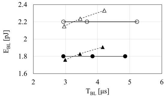
Figure 9.
Performance comparison between SBL and ABL. Symbols are defined in Table 1.
3. BL Path Design: Conventional vs. Proposed
3.1. Circuits
Figure 10a,b illustrate conventional and proposed circuits in a BL path, respectively. In the proposed circuit, a power switch is added to the conventional circuit in order to supply VDDBL from an internal VDD (VDDint) to VDD or vice versa.
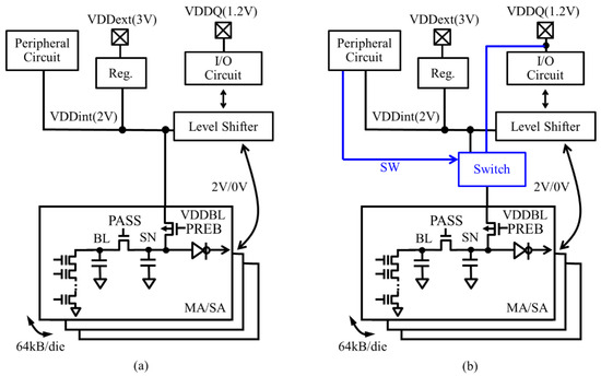
Figure 10.
Conventional (a) and proposed (b) circuits in a BL path. The arrows indicate the data path between SA and the level shifters.
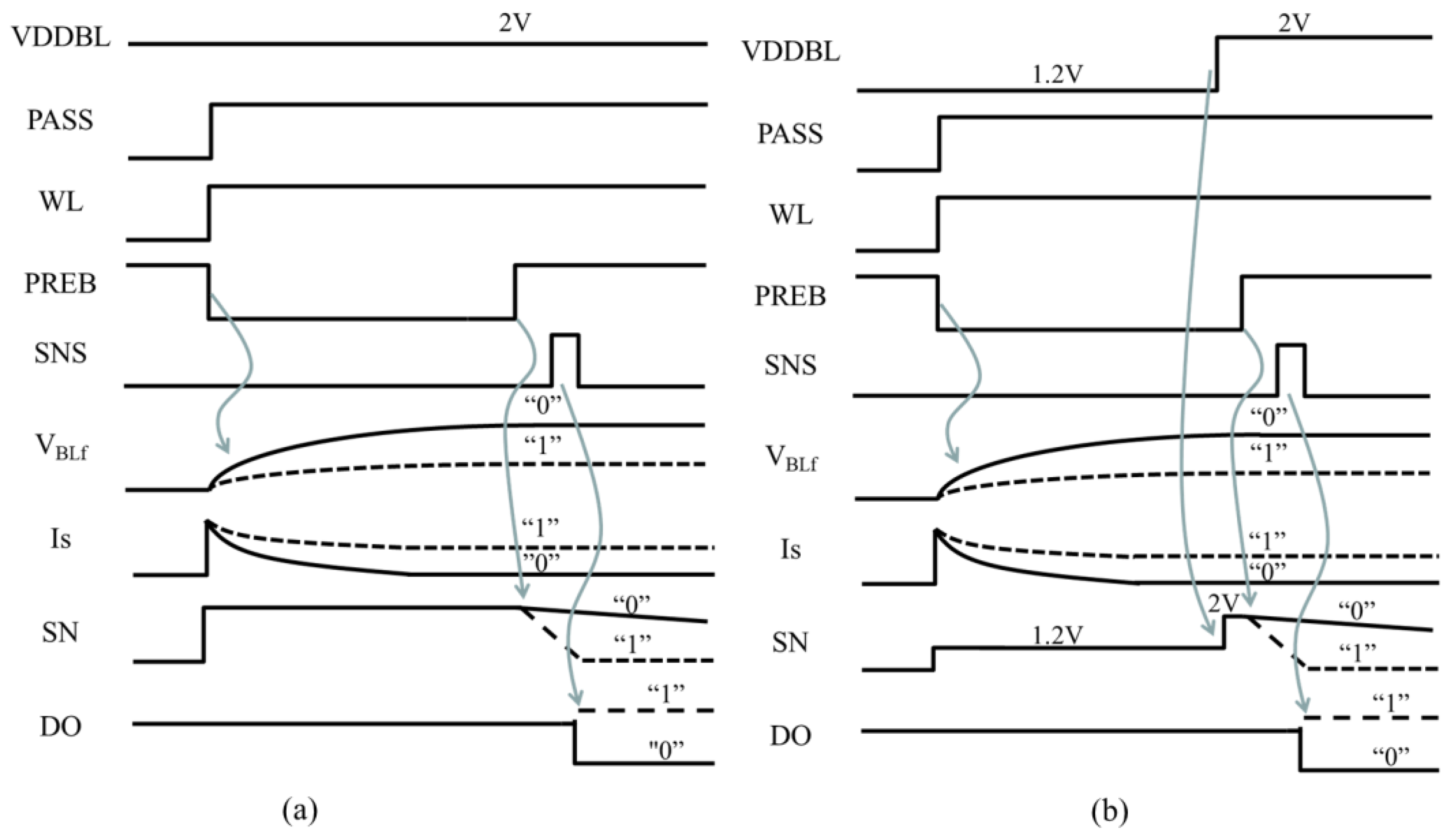
Figure 11a,b show the read operation waveforms of the conventional (a) and proposed (b) circuits, respectively. The differences in the operation of the proposed circuit are that (1) VDDBL is switched to VDDQ during BL pre-charge with PREB low to reduce the power to BLs, and (2) the SN voltage is boosted up to 2 V after the pre-charge operation, before sensing, by switching VDDBL to VDDint to keep the SN voltage as high as that in the conventional circuit, maintaining a sense margin which is defined by the voltage difference at SN between “1” and “0”. The N-well of PREB transistors can be switched from VDDQ to VDDint in 100 ns. The access overhead of the proposed design is about 2% when the BL access time of the conventional design is 5 μs.
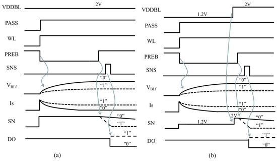
Figure 11.
Read operation waveform of conventional (a) and proposed (b) circuits. The arrows indicate signal propagation. The dash lines show the signals for “1”-date.
3.2. Energy in the BL Path
The energy during the pre-charge period (EP) and the sense period (ES) of the conventional design are given by (17) and (18), respectively. (Note that power supplies are disconnected in the sense period).
Therefore, the total energy per read cycle (EBL) is estimated by (19).
In the case of the proposed design, (20) and (21) hold, instead of (17) and (18).
As a result, the total energy per read cycle of the proposed design is estimated by (22).
To estimate how much energy can be reduced with the proposed design in the worst case scenario and compare the estimates with the SPICE results, the parameters in Table 2 are used. The EP and ES of the conventional design are 6.7 pJ and 0 pJ, whereas those of the proposed one are 2.6 pJ and 0.3 pJ. As a result, the EBL is estimated to be 6.7 pJ for the conventional design and 2.9 pJ for the proposed one. A reduction in energy of 56% mainly comes from the difference in the most significant first terms of (19) and (22).
Table 2.
Device and design parameters used for the circuit design.
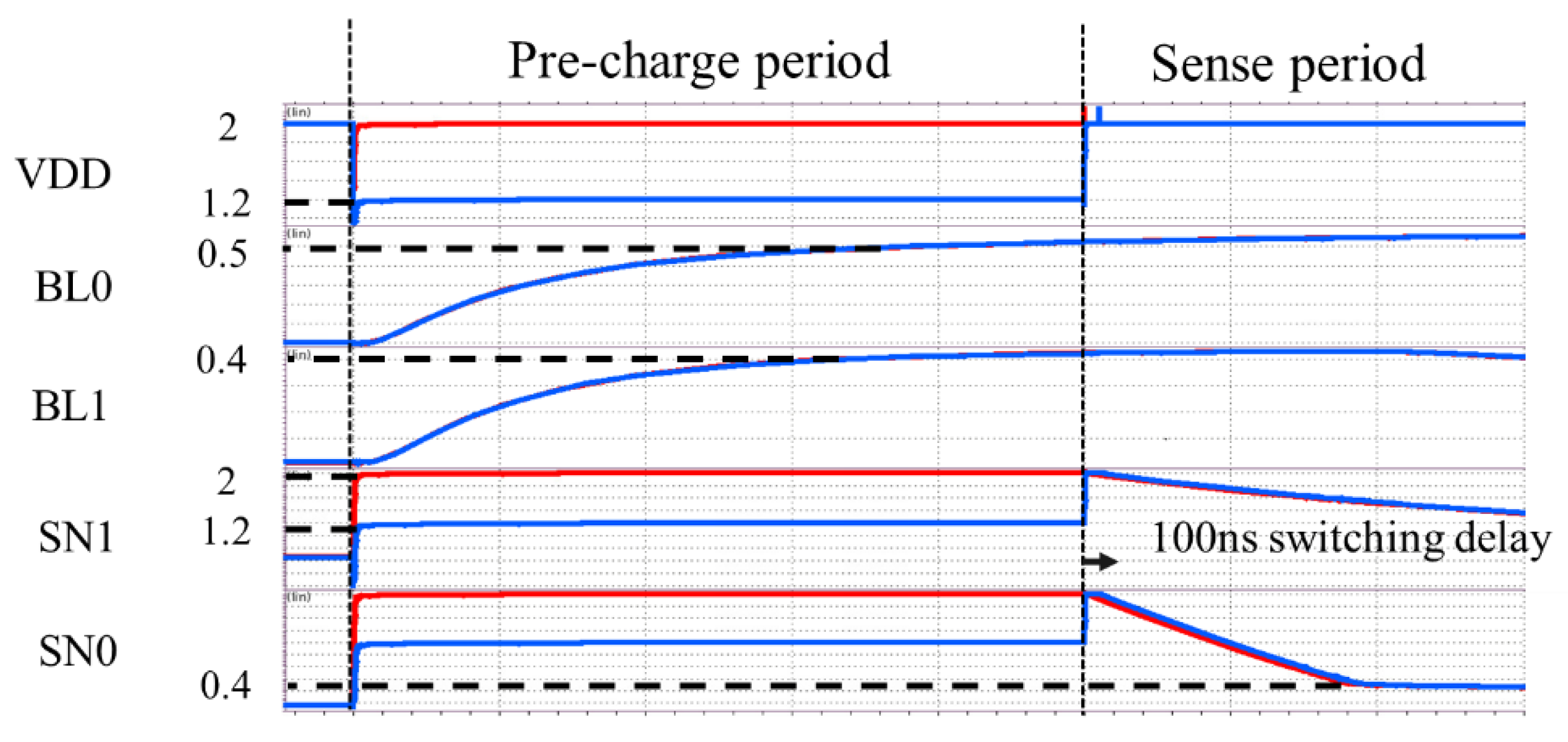
Figure 12 shows the SPICE waveforms of the conventional (in red) and proposed (in blue) designs. The energy in the operation cycle are 6.6 pJ and 3.0 pJ, respectively. A reduction of 55% was confirmed with SPICE.
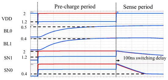
Figure 12.
Comparison of SPICE waveform: conventional in red and proposed in blue. The dashed lines are added in the original captured SPICE waveform to show the voltage levels.
In the above explanation, the proposed design was based on all-bit-line sensing [21], but it is also effective when based on other designs such as shielded-BL sensing [22] and improved sensing [23,24]. Thus, the proposed circuit can be used commonly.
4. Experimental
To validate the effectiveness of the proposed design on power reduction, a test circuit was designed and fabricated in 180 nm CMOS, as shown in Figure 13. In an actual NAND Flash memory, parasitic BL resistance and capacitance are based on the nature of the wiring. In this test circuit, a poly resistor and an MIM capacitor were used to mimic parasitic BL resistance and capacitance. Without the memory process, normal NMOSFETs were used as cell transistors. To have ICELL1 and ICELL0 with a normal NMOSFET, the WL voltage (i.e., gate voltage of the transistors) was altered between high and low. Equivalently, 100 sets of BLs and sense amp were implemented. A sufficiently small area was required for the power switch. Analog buffers were placed next to the BLs to monitor VBL at different locations.
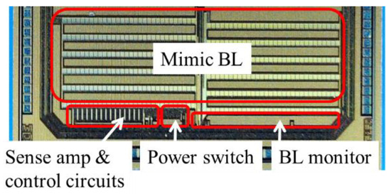
Figure 13.
Die photo.
Figure 14a illustrates an analog buffer. To monitor VBL in the range between 0 V and 0.5 V, PMOSFET is used as a source follower amp. Because 3 V transistors are available in 180 nm CMOS, a VDDMON of 3 V is sufficient to monitor VBL up to 1 V, as shown in Figure 14b.
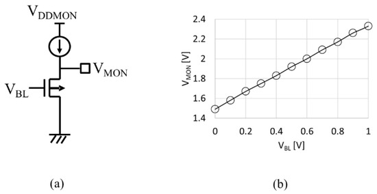
Figure 14.
Analog buffer (a) and VBL(VMON) characteristics (b).
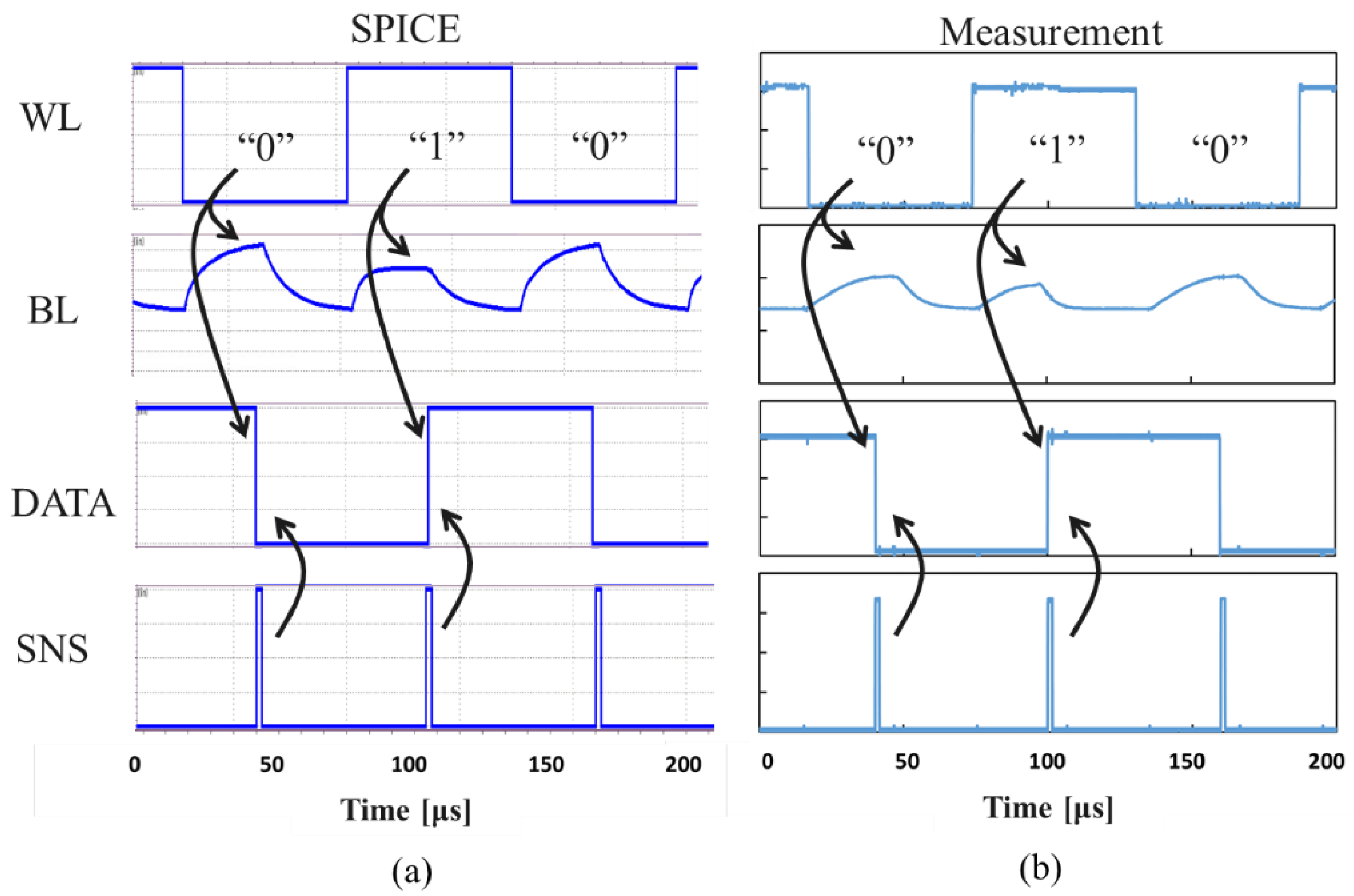
To estimate the energy of the conventional design, the power switch was not toggled to force VDDBL with VDDint in entire cycles. Figure 15 shows the waveform in the case of 0-1-0 access with a cycle time of 60 μs in the proposed circuit mode. Due to the insufficient tail current of the fabricated analog buffers, the cycle time needed to be longer than expected to accurately measure the energy. Therefore, the energy in a cycle time of 5 μs was estimated using the data in Figure 16. The estimated energy for a 5 μs read cycle was 1.3 nJ in the case of the conventional circuit mode and 0.54 nJ in the case of the proposed circuit mode. As a result, a reduction in energy of 59% was achieved.
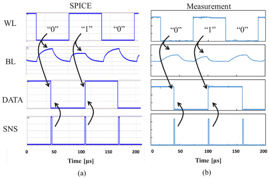
Figure 15.
(a) Simulated and (b) measured waveforms. The arrows show signal transition.
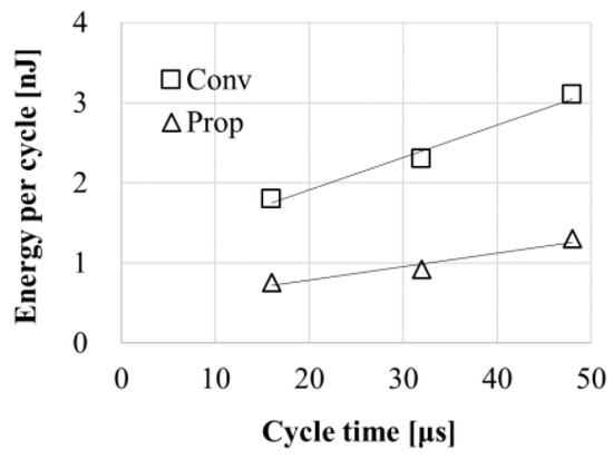
Figure 16.
Energy per cycle vs. cycle time.
5. Design Consideration
Every NAND product has a specific BL capacitance and a specific energy ratio of BL path to WL path. Section 5.1 and Section 5.2 discuss energy as a function of BL capacitance and the average drive energy as a function of the energy ratio of the BL path to the WL path, respectively. In addition, immunity against noise in VDDQ is presented in Section 5.3. The impact of capacitive coupling between adjacent nodes is part of the work remaining, which is further specified in Section 5.4.
5.1. Energy vs. BL Capacitance
In Section 3 and Section 4, a C of 3 pF was assumed for the validation of the proposed design. This value can vary by product when the BL length is longer or shorter, depending on the number of blocks per die. The value can also be different in terms of technology, when the thickness, width, or space of the BL wires is varied. Figure 17a shows the energy for one BL path in a single read operation as a function of C. Figure 17b shows the reduction rate obtained with the proposed design over the conventional one. As discussed in Section 3, EBL has the components of C, VBL, and VSupply and ICELL, TC, and VSupply. As long as the first component is the majority, the reduction rate in EBL does not significantly depend on C. Figure 17b indicates that the proposed design can be effective over various products with different Cs.
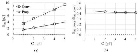
Figure 17.
(a) Energy vs. C and (b) reduction rate vs. C.
5.2. Average Die Energy vs. Energy Ratio of BL Path to WL Path
How much energy consumption is reduced by with the proposed design depends on the value of VDDQ. In addition, the average die energy is the sum of the energy for the BL and WL paths when the rest can be negligibly, relatively small. The energy ratio of the BL path to the WL path depends on the array configuration, which varies by product. Thus, the reduction in the average die energy with the proposed BL path design is a function of VDDQ and the energy ratio of the BL path to the WL path. Figure 18 shows the average die energy normalized by that of ONFI 1.0 NAND with 3 V VDDQ. Three cases with respect to the energy ratio (EBL:EWL) are studied, with 1:2, 1:1, and 2:1. As expected, the average die energy is reduced as VDDQ is reduced from 3 V in ONFI 1.0 to 1.8 V in ONFI 2.0 and to 1.2 V in ONFI 3.0 and 4.0, regardless of the energy ratio of the BL path to the WL path. As long as VDDQ is high enough to operate PASS transistors in the saturation region at a VBL of 0.5 V, even at a low VDDQ of 0.8 V, normal BL path operation and energy reduction can be observed in the SPICE results. The reduction in the average die energy with the proposed design is estimated to be about 22% for the 1:2 case, 33% for the 1:1 case, and 46% for the 2:1 case. As a result, the proposed design can still be effective for NAND products with different VDDQs and different energy ratios of BL path to WL path.
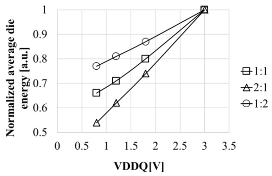
Figure 18.
Normalized energy vs. VDDQ.
5.3. Immunity against Noise in VDDQ
Because VDDQ is the supply voltage for IO buffers, it has a noise generated from IO operation. Another design concern is how much VBL is affected by such a noise in the VDDQ during the pre-charge period. SPICE simulations were run with single-tone noises whose frequencies ranged from 1 kHz to 1 GHz. PASS transistors operating in the saturation region had a sufficiently large drain-to-source impedance, with a 40 dB rejection ratio, which means that the VBL varies by 1 mV when a ripple in the VDDQ is 100 mV. As a result, NAND dies following the proposed design could work even in severe environments of heavy traffic in the IO data paths of SSDs. When the PASS signal line is routed in parallel with the VDDQ line, layout designers need to add a shielding line between the two with sufficiently low impedance.
In this paper, it is assumed that the NAND interface does not change to eliminate the additional cost for designing and producing new printed circuit boards. However, when the cost for powering the SSD becomes quite significant, especially for data centers, an additional lower voltage supply, such as 0.8 V, dedicated to BL charging for read and program verifying operations may be the best option for future applications.
5.4. Remaining Work: Impact of Capacitive Coupling between Adjacent Nodes
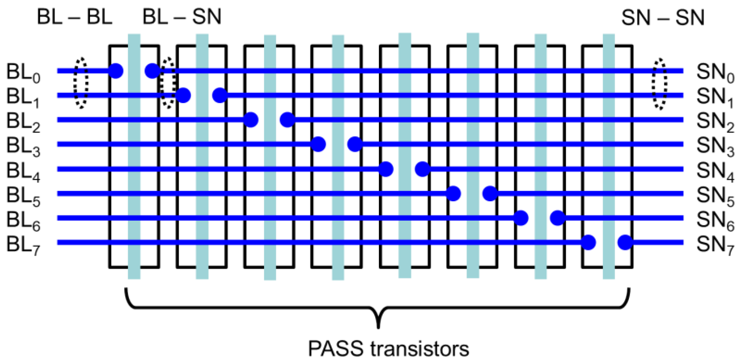
In this paper, the model has been developed under the assumption that next-neighbor BLs are short to the ground (to be replaced with redundancy BLs), which determines TBL based on the largest BL capacitance. In this case, the developing time for SN nodes of 100 ns was sufficient. Figure 19 illustrates a layout example of eight next-neighbor sense amplifiers. In addition to BL–BL coupling, there are BL–SN coupling and SN–SN coupling, as marked. The overlapped length between a BL and an SN can be as short as 1 μm, which would have no significant capacitive coupling to the sensing operation. On the other hand, the overlapped length between adjacent SN nodes can be much longer. For a “0”—BL whose next-neighbor BLs are connected with 1-cell, strong capacitive coupling may decrease the SN voltage below the threshold of the sense amplifier. In this situation, a capacitor needs to be added at every SN node intentionally in order to reduce such a coupling effect. The additional capacitance will increase the delay time for SN nodes. As a result, the assumed delay time of 100 ns in this work can be much longer. It is necessary to revise the circuit model to include capacitively coupling effects between adjacent BLs and sense amplifiers in future works.
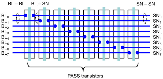
Figure 19.
Layout example for multiple sense amplifiers.
6. Summary
A low-power design in the BL path of NAND Flash was proposed and validated. A reduction in the entire energy demand per die of 20% to 40% can be expected for ONFI 3 or 4 NAND Flash with a VDDQ of 1.2 V, depending on the energy ratio between BL and WL paths, in comparison to conventional BL path operations. The overheads of a delay time in the BL path of 2% and an area of the additional power switch of 0.1% are drawbacks but can be considered small enough against the significant energy reduction obtained using the proposed method. Further reductions with the proposed design will be possible for future NANDs through lower VDDQs or by introducing an additional lower-voltage supply dedicated to BL charging for read and program verifying operations.
Author Contributions
Conceptualization, T.T.; methodology, H.M. and T.T.; software, H.M.; validation, H.M. and T.T.; formal analysis, H.M. and T.T.; investigation, H.M. and T.T.; writing—original draft preparation, H.M.; writing—review and editing, T.T.; funding acquisition, T.T. All authors have read and agreed to the published version of the manuscript.
Funding
This research was partially funded by Kioxia Corp.
Data Availability Statement
Data are contained within the article.
Conflicts of Interest
The authors declare no conflicts of interest.
References
- Masanet, E.; Shehabi, A.; Lei, N.; Smith, S.; Koomey, J. Recalibrating global data center energy-use estimates. Science 2020, 367, 984–986. [Google Scholar] [CrossRef] [PubMed]
- Pelley, S.; Meisner, D.; Wenisch, T.F.; VanGilder, J.W. Understanding and Abstracting Total Data Center Power. Workshop on Energy-Efficient Design. 2009, Volume 11, pp. 1–6. Available online: https://www.yumpu.com/en/document/read/6834164/understanding-and-abstracting-total-data-center-power-dept-of- (accessed on 24 January 2024).
- Info-Tech. Top 10 Energy-Saving Tips for a Greener Data Center; Info-Tech Research Group: London, ON, Canada, 2010; Available online: http://static.infotech.com/downloads/samples/070411_premium_oo_greendc_top_10.pdf (accessed on 20 January 2024).
- Uzaman, S.K.; Shuja, J.; Maqsood, T.; Rehman, F.; Mustafa, S. A systems overview of commercial data centers: Initial energy and cost analysis. Int. J. Inf. Technol. Web Eng. (IJITWE) 2019, 14, 42–65. [Google Scholar] [CrossRef]
- Pakbaznia, E.; Ghasemazar, M.; Pedram, M. Temperature-aware dynamic resource provisioning in a power-optimized datacenter. In Proceedings of the 2010 Design, Automation & Test in Europe Conference & Exhibition (DATE 2010), Dresden, Germany, 8–12 March 2010; IEEE: New York, NY, USA; pp. 124–129. [Google Scholar]
- Pelley, S.; Meisner, D.; Zandevakili, P.; Wenisch, T.F.; Underwood, J. Power routing: Dynamic power provisioning in the data center. ACM SIGARCH Comput. Archit. News 2010, 38, 231–242. [Google Scholar] [CrossRef]
- Abts, D.; Marty, M.R.; Wells, P.M.; Klausler, P.; Liu, H. Energy proportional datacenter networks. In Proceedings of the 37th Annual International Symposium on Computer Architecture, Saint-Malo, France, 19–23 June 2010; pp. 338–347. [Google Scholar]
- Tsirogiannis, D.; Harizopoulos, S.; Shah, M.A. Analyzing the energy efficiency of a database server. In Proceedings of the 2010 ACM SIGMOD International Conference on Management of Data, Indianapolis, IN, USA, 6–11 June 2010; pp. 231–242. [Google Scholar]
- Dayarathna, M.; Wen, Y.; Fan, R. Data center energy consumption modeling: A survey. IEEE Commun. Surv. Tutor. 2015, 18, 732–794. [Google Scholar] [CrossRef]
- Mohan, V.; Bunker, T.; Grupp, L.; Gurumurthi, S.; Stan, M.R.; Swanson, S. Modeling power consumption of nand flash memories using flashpower. IEEE Trans. Comput.-Aided Des. Integr. Circuits Syst. 2013, 32, 1031–1044. [Google Scholar] [CrossRef]
- M550 M.2 Type 2280 NAND Flash SSD. Available online: https://www.micron.com/-/media/client/global/documents/products/data-sheet/ssd/m550_m2_2280_ssd.pdf (accessed on 24 January 2024).
- Siau, C.; Kim, K.H.; Lee, S.; Isobe, K.; Shibata, N.; Verma, K.; Ariki, T.; Li, J.; Yuh, J.; Amarnath, A.; et al. 13.5 A 512 Gb 3-bit/cell 3D flash memory on 128-wordline-layer with 132 MB/s write performance featuring circuit-under-array technology. In Proceedings of the 2019 IEEE International Solid-State Circuits Conference-(ISSCC), San Francisco, CA, USA, 17–21 February 2019; IEEE: New York, NY, USA, 2019; pp. 218–220. [Google Scholar]
- ONFI. Available online: https://www.onfi.org/ (accessed on 24 January 2024).
- Toggle. Available online: https://www.jedec.org/category/keywords/toggle (accessed on 24 January 2024).
- Yuh, J.; Li, J.; Li, H.; Oyama, Y.; Hsu, C.; Anantula, P.; Jeong, S.; Amarnath, A.; Darne, S.; Bhatia, S.; et al. A 1-Tb 4b/Cell 4-Plane 162-Layer 3D Flash Memory with a 2.4-Gb/s I/O Speed Interface. In Proceedings of the IEEE International Solid-State Circuits Conference (ISSCC), San Francisco, CA, USA, 20–26 February 2022. [Google Scholar] [CrossRef]
- Lassa, P. The New EZ NAND in ONFI v2.3. In SanDisk-Flash Memory Summit-Aug; SanDisk: Milpitas, CA, USA, 2010. [Google Scholar]
- Tripathy, S.; Sahoo, D.; Satpathy, M.; Pinisetty, S. Formal modeling and verification of nand flash memory supporting advanced operations. In Proceedings of the 2019 IEEE 37th International Conference on Computer Design (ICCD), Abu Dhabi, United Arab Emirates, 17–20 November 2019; IEEE: New York, NY, USA, 2019; pp. 313–316. [Google Scholar]
- Tanzawa, T.; Tanaka, T.; Takeuchi, K.; Nakamura, H. Circuit techniques for a 1.8-V-only NAND flash memory. IEEE J. Solid-State Circuits 2002, 37, 84–89. [Google Scholar] [CrossRef]
- Gonugondla, S.K.; Kang, M.; Kim, Y.; Helm, M.; Eilert, S.; Shanbhag, N. Energy-efficient deep in-memory architecture for NAND flash memories. In Proceedings of the 2018 IEEE International Symposium on Circuits and Systems (ISCAS), Florence, Italy, 27–30 May 2018; IEEE: New York, NY, USA, 2018; pp. 1–5. [Google Scholar]
- Makino, H.; Tanzawa, T. A 30% Power Reduction Circuit Design for NAND Flash by Utilizing 1. 2 V I/O Power Supply to Bitline Path. In Proceedings of the IEEE the 18th Asia Pacific Conference on Circuits and Systems, Shenzhen, China, 11–13 November 2022. [Google Scholar]
- Tanaka, T.; Tanaka, Y.; Nakamura, H.; Sakui, K.; Oodaira, H.; Shirota, R.; Ohuchi, K.; Masuoka, F.; Hara, H. A quick intelligent page-programming architecture and a shielded bitline sensing method for 3 V-only NAND flash memory. IEEE J. Solid-State Circuits 1994, 29, 1366–1373. [Google Scholar] [CrossRef]
- Cernea, R.A.; Pham, L.; Moogat, F.; Chan, S.; Le, B.; Li, Y.; Tsao, S.; Tseng, T.-Y.; Nguyen, K.; Li, J.; et al. A 34 MB/s MLC write throughput 16 Gb NAND with all bit line architecture on 56 nm technology. IEEE J. Solid-State Circuits 2009, 44, 186–194. [Google Scholar] [CrossRef]
- Huh, H.; Cho, W.; Lee, J.; Noh, Y.; Park, Y.; Ok, S.; Kim, J.; Cho, K.; Lee, H.; Kim, G.; et al. 13.2 a 1Tb 4b/Cell 96-Stacked-WL 3D NAND Flash Memory with 30MB/s Program Throughput Using Peripheral Circuit under Memory Cell Array Technique. In Proceedings of the 2020 IEEE International Solid-State Circuits Conference-(ISSCC), San Francisco, CA, USA, 16–20 February 2020. [Google Scholar]
- Kim, C.; Kim, D.H.; Jeong, W.; Kim, H.J.; Park, I.H.; Park, H.W.; Lee, J.; Park, J.; Ahn, Y.-L.; Lee, J.Y.; et al. A 512-Gb 3-b/Cell 64-Stacked WL 3-D-NAND Flash Memory. IEEE J. Solid-State Circuits 2018, 53, 124–133. [Google Scholar] [CrossRef]


Disclaimer/Publisher’s Note: The statements, opinions and data contained in all publications are solely those of the individual author(s) and contributor(s) and not of MDPI and/or the editor(s). MDPI and/or the editor(s) disclaim responsibility for any injury to people or property resulting from any ideas, methods, instructions or products referred to in the content. |
© 2024 by the authors. Licensee MDPI, Basel, Switzerland. This article is an open access article distributed under the terms and conditions of the Creative Commons Attribution (CC BY) license (https://creativecommons.org/licenses/by/4.0/).