1. The Need for Intelligent Sampling Approaches
The expansion of the Internet of Things (IoT) has brought forth an explosion in the number of wireless sensor node (WSN) applications; the WSN market [
1] is currently growing by 15.5% annually. The primary objective of a WSN (
Figure 1a) is to efficiently encode observations of physical phenomena into digital symbols for wireless transmission to a base station. Nearly all application scenarios of WSNs are resource-constrained, and WSN designers must intelligently balance power usage, data integrity, and system adaptability, which are, in turn, dependent on both the input signal and the signal processing pipeline. Biomedical applications, such as wearables and implantable devices [
2,
3,
4,
5], are particularly challenging since they have stringent upper bounds on device size and power consumption.
To obtain approximate design constraints for implantables, we consider intracortical neural recorder arrays. The volume of packaged arrays must be a few
or less. For typical die areas (roughly 30 mm
2), intracortical neural recorder arrays have a power limit of roughly 10
to prevent damage to brain tissue [
6]. The low-noise amplifiers (LNAs) required in the analog front end consume 20–30% of the total power in a typical neural recorder power budget, while wireless transmission and the analog–digital converters (ADCs) have a combined 40–50% contribution to the total power [
6,
7].
Modern ADCs perform at efficiencies exceeding 1
/Mbps [
8], yet simply connecting the ADC output to a standard digital pad, which can present up to 100
capacitance (at VDD = 1
), would require 50
/Mbps. In fact, the power consumption of wireless transmission and ADCs can range from 100
/Mbps for backscatter communication to 10
/Mbps for short-range frequency-shift keying (FSK) transmission [
6,
7]. Bluetooth low energy 5 (BLE 5) and similar commercial standards need roughly 50
/Mbps at 8 dBm transmit power [
9].
Improvements in LNA power consumption and data transmission cost are fundamentally bottlenecked by gain and noise requirements [
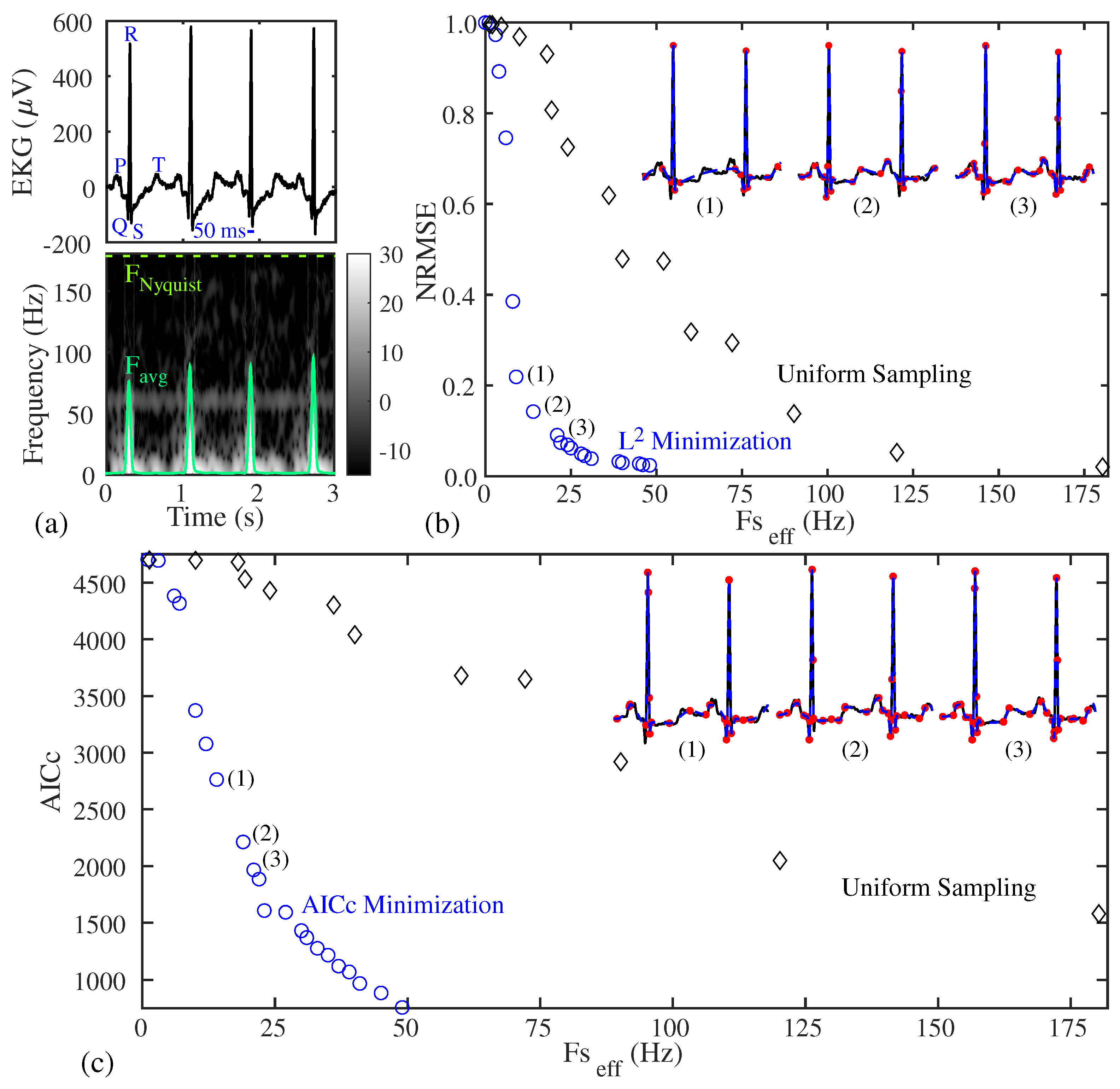
6]. Nevertheless, not all sensor data are relevant, and one can greatly benefit from reducing the transmitted data. However, data reduction approaches must not cause the excessive loss of information or require excessive resource overhead. Biological signals, epitomized by electrocardiograms (ECGs) (
Figure 2a), are often non-stationary [
10,
11,
12]. To accurately capture the rapid transients of the QRS complexes (marked in
Figure 2a), which usually persist for less than 20% of the inter-heartbeat period, sampling rates of at least 250
and resolutions of at least 8 bit are essential [
13,
14]. This non-stationary characteristic opens up the possibility of utilizing nonuniform sampling to significantly reduce the number of transmitted data points at the source without requiring complex data compression approaches.
The relevance of nonuniform sampling stretches beyond its conventional applications in sensing into physical computation applications. Solutions derived from biologically inspired ordinary differential equations (ODEs) frequently exhibit non-stationary signals. Due to the analogous behavior of metal-oxide-semiconductor field-effect transistors (MOSFETs) and biological channels, these biologically inspired ODEs can often be computed physically with less power than is needed for sampling the solution at the necessary speed and precision [
15]. Consequently, the same incentives for the nonuniform sampling of physiological signals are applicable to the digital readout of ODE solutions on analog hardware accelerators.
This work, which builds on [
16], proposes an extrema pulse generator which is capable of triggering an ADC (like an asynchronous successive approximation register (SAR)) at significant extrema and a timer to capture the corresponding timestamps (
Figure 1b). While extrema sampling is a versatile, theoretically justified nonuniform sampling method, its practical use requires the development of more robust hardware and software than those currently available. In contrast to the limited number of previous hardware approaches [
17,
18] that have demonstrated low-power extrema detection circuits and signal reconstruction from extrema points, our work presents the following enhancements and technical contributions:
A comprehensive discussion justifying extrema sampling using signal-theoretic principles and two naive nonuniform sampling approaches.
A novel extrema pulse generator circuit design that is readily adaptable for scenarios with differing operating frequencies, power budgets, and signal-to-noise ratios (SNRs).
A reconstruction algorithm that is resilient to circuit nonideality and allows for a more relaxed set of assumptions about the interpolation function.
Experimental verification of the Pareto optimality of extrema sampling over uniform sampling for two test signals.
We construct the extrema pulse generator and experimentally demonstrate its performance using an system-on-chip (SoC) field-programmable analog array (FPAA) previously fabricated in a 350
complementary MOS process at Georgia Institute of Technology [
19]. The rest of this work is structured as follows:
Section 2 justifies the reasons for using extrema sampling as opposed to other nonuniform sampling approaches,
Section 3 provides a brief overview of the SoC FPAA infrastructure,
Section 4 presents an in-depth analysis of the subcircuits composing the extrema pulse generator,
Section 5 explains the signal reconstruction process,
Section 6 offers a comparative analysis of the system’s performance against other sampling methods, and
Section 7 offers concluding remarks.
2. Nonuniform Sampling Approaches
A primary reason for the high energy efficiency of the human sensory nervous system is that it is only sensitive to
novel events [
20]. Nonuniform sampling approaches typically employ similar event-driven strategies to improve energy efficiency and reduce the need for energy-intensive compression algorithms and the data transmission cost in WSNs. Most nonuniform sampling approaches [
21,
22,
23,
24,
25,
26,
27] leverage extra assumptions or information about signal features (besides the spectral support range) to sample more intelligently. Each nonuniform sampling approach comes with its own set of challenges, tradeoffs, and assumptions. As a result, nonuniform sampling approaches are often highly application-specific, posing a barrier to the commercial availability of nonuniform ADCs. Even in academic settings (e.g., clinical studies), a priori information about the signal features of interest can be limited, so a feature-specific sampling approach may cause the undesired loss of information. It is illuminating to analyze contemporary nonuniform sampling approaches before discussing extrema sampling.
Application-specific event-detectors usually wake up a microcontroller to sample an ADC when an interesting event is detected (such as acoustic spectra from a vehicle [
27]). This approach performs well when interesting events are rare, since high-power components can be kept in sleep states for prolonged periods while an always-on, low-power classifier monitors for interesting events. Yet, as interesting events become more frequent, the benefits gleaned by application-specific event-detectors become less pronounced [
27] and are eventually overcome by the additional hardware overhead. Low-power event classifiers are often heavily limited in scope and require meticulous retraining for a different event class.
Level-crossing ADCs [
22], which generalize the principle of event detection, sample the input signal when it changes by some multiple of a least sensitive bit. Level-crossing ADCs map the problem of precision voltage measurement at uniform time steps to the often easier problem of precision time measurement as the input crosses (usually uniformly spaced) reference voltages. Level-crossing ADCs are expected to scale well since time–digital converter precision and energy efficiency improve with decreasing technology node [
28]. Although there have been efforts to mitigate this [
25,
26], level-crossing ADCs tend to oversample many classes of signals, especially if good voltage resolution is required.
If it is known a priori that the signal to be sampled has a sparse representation in some transform domain, then the signal can be acquired by random sampling approaches widely known as compressive sampling. Compressive sampling has been immensely successful in the recovery of many natural signals far below their Nyquist rate. Yet, a major demerit of compressive sampling lies in signal recovery, where a convex optimization problem (typically L
1 norm minimization) must be solved [
23,
24]. The best case overhead for L
1 minimization [
29] tends to be higher than that of Lagrange [
30,
31] or cubic [
32] interpolation. Furthermore, the convergence time of the recovery algorithm in compressive sensing, which is uncertain (as opposed to interpolation-based approaches), can be problematic for real-time or closed-loop applications.
To summarize, the events identified by a nonuniform sampling methodology range in complexity from simple input value changes, as in level-crossing ADCs, to complex, signal-specific features identified by techniques like spectral template matching [
27], as in application-specific event detectors. While the former method offers higher sensitivity with a lower component count (albeit with lower specificity), the latter approach provides higher specificity, but with lower sensitivity and an increased number of components. In contrast, our proposed approach, extrema sampling, is a broadly applicable solution that reduces energy usage with both a low component count and low reconstruction error.
Indeed, extrema sampling, in contrast to the previously mentioned methods, relaxes signal-specific assumptions, offering a framework applicable to a wide array of scenarios. Sampling at twice the mean frequency of the input signal, extrema sampling often samples considerably below the global Nyquist rate for non-stationary signals (even after accounting for the two-fold penalty associated with also acquiring sample timestamps). Moreover, extrema sampling does not necessitate costly signal reconstruction algorithms and is grounded [
21] in theory since
In addition to the established reasons described above, in this work, we also show that extrema sampling arises naturally from the solution of a few types of optimization problems. The first problem we propose is the selection of time-domain points so as to minimize the polynomial reconstruction error subject to a constraint on the mean sampling rate (
). We formulate this first problem as the following constrained nonlinear integer programming problem, which we solve using a genetic algorithm:
Normalized root-mean-square error (NRMSE) is an estimate of the error between the original ECG data vector (
) and the reconstructed data vector (
), guided by a vector (
) of length
n containing binary elements which decide which of the
n elements of
to sample. It can be shown that the definition of NRMSE in this work, which was proposed previously in [
15], is equivalent to the root-mean-square reconstruction error normalized by the standard deviation of the truth (original ECG data). While solving Equation (
1), we ensure
is highly oversampled so as to approximate a continuous-time signal, and we reconstruct
using a piecewise cubic Hermite interpolating polynomial (PCHIP) function.
The Pareto fronts (please see [
34] for a detailed discussion on Pareto fronts and optimality) obtained for uniform and nonuniform ECG sampling (as determined by solving Equation (
1)) are shown in
Figure 2b. As shown in
Figure 2b, our naive nonuniform sampling approach has a tendency to prioritize significant signal extrema, which allows the nonuniform method to reconstruct ECGs using a fewer number of sample points and with a lower reconstruction error (NRMSE) than the uniform sampling approach (i.e., achieving a Pareto optimal tradeoff between NRMSE and the effective sampling rate
relative to uniform sampling). The optimality advantage of nonuniform sampling remains even if the extra overhead needed to acquire timestamps in the nonuniform case is considered.
Our second proposed problem is the selection of time-domain points so as to minimize a model-selective, information-theoretic criterion subject to a constraint on the mean sampling rate (
). We formulate this second problem as the following constrained nonlinear integer programming problem, which is also solved using a genetic algorithm:
The number and selection of sample points on the time-domain waveform corresponds to the selection of the PCHIP model order and a choice of parameters. AICc denotes the Akaike Information Criterion corrected for small sample sizes, which is a widely used information-theoretic model selection criterion [
35,
36] that rewards models with lower mean-squared error while appropriately penalizing models with a larger number of model parameters (
k) and adding a correction term for small sample sizes. In our mathematical formalism, AICc can be written as follows [
36]:
The optimization results of Equation (
2) are shown in
Figure 2c. We see similar results in
Figure 2b, where the AICc minimization demonstrates that an intelligent choice of time-domain sample points leads to a precise, yet more parsimonious, representation of a signal than a uniformly sampled set of points. Additionally, like in
Figure 2b, the optimal sample points also predominantly include extrema.
The efficacy of signal reconstruction from extrema samples is contingent on a proper selection of reconstruction basis. The discussion in the preceding paragraph suggests that, for certain smooth signals like ECGs, PCHIPs are a good choice of basis function because PCHIPs enforce continuity and smoothness conditions. However, for signals with abrupt changes or corners, such as a sawtooth wave, a different basis function (e.g., a linear interpolation method) could be more effective, offering accurate reconstructions without the need for complex algorithms. It should be noted that signals that are contaminated with high-frequency noise beyond signal frequencies should be prefiltered before extrema sampling to mitigate false positives. False positives do not constitute data loss and thus would not degrade reconstruction quality given an a posteriori assessment of which data points correspond to false positives (e.g., using a method we show in
Section 5). However, the occurrence of false positives would diminish the data savings gained through extrema sampling, thereby increasing the mean effective sampling rate to a value that is closer to the Nyquist rate.
3. SoC FPAA Infrastructure
To construct our circuits, we use an SoC field-programmable analog array FPAA developed at Georgia Institute of Technology. The SoC FPAA is a highly versatile general-purpose analog computing platform in a 350
process [
19]. The FPAA uses software tools that are openly available at hasler.ece.gatech.edu/FPAAtool/ and has 98 fully reconfigurable computational analog blocks (CABS) that are interconnected with a programmable, nonvolatile routing fabric comprising floating-gate (FG) transistors (
Figure 3).
Each CAB contains a wide assortment of analog computational elements: operational transconductance amplifiers (OTAs), floating-gate OTAs (FGOTAs), discrete transistors, capacitors, current mirrors, and T-gates, which can be interconnected to synthesize larger circuits. Synthesized circuits can be either contained within a CAB or span multiple CABs.
The routing fabric of the FPAA is used to make flexible nonvolatile connections or to generate nonvolatile subcircuit current biases with 13-bit precision [
37] using roughly half-a-million FG transistors. An FG transistor is a MOSFET with only capacitors tied to the gate. In this way, the gate of a FG is floating, with no DC connection to any other node, which allows charge to be trapped on the gate. One of these gate capacitors (typically a MOS capacitor) is used to remove electrons from the FG through Fowler–Nordheim tunneling across its insulator. The other capacitors, which typically have a higher coupling factor to the FG than the MOS capacitor, are control gates. The control gates are particularly useful during hot electron injection, a process by which electrons can be injected into the FG through the gate oxide of the FG transistor. FG transistors allow circuit designers a great level of control over transistor IV curves and can be used to mitigate manufacturing mismatch.
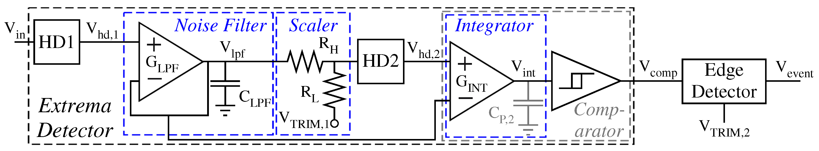
4. Extrema Pulse Generator
Comprising two subcircuits, the extrema detector and the edge detector, our proposed low-power extrema pulse generator is shown in
Figure 4. The objective of the extrema detector is to change its output state at the input extrema. The edge detector then produces an active-low pulse given a state change on the extrema detector output. The hysteretic differentiator (HD) is pivotal to the overall extrema detector circuit; thus, it is imperative to first elucidate the HD operation.
4.1. Hysteretic Differentiator
In order to detect extrema, one must perform edge detection using some sort of differentiation operation. However, the noise immunity of linear differentiators is poor [
20]. In a fundamental sense, differentiators are circuits whose outputs are insensitive to the absolute voltage level of the signal while remaining sensitive to the local signal derivative. The functionality of our extrema detector is contingent on the HD (
Figure 5a), a nonlinear differentiator circuit [
20] which is tolerant to noise.
In essence, the structure of the HD is analogous to a voltage follower comprising a nonlinear buffer stage that is driven by OTA , which is biased via an FG pFET. The output of the HD () corresponds to the output of . For a small HD input (), the output swing of the buffer stage is also small, and the buffer can be approximated as a linear system; thus, tracks closely given a small . In contrast, is sensitive to when is large, transitioning sharply at signal extrema since the dominant FET swaps; given the unconventional positioning of the transistors (pFET drain at ground and nFET drain at Vdd), the swap of the dominant FET requires a large change in the common gate control voltage to source or sink an appreciable amount of current. Note that the pFET is dominant for decreasing , and the nFET is dominant for increasing .
4.2. Extrema Detector Circuit
While the HD can generate sharp transitions upon observing extrema, the output transients of an HD are slow if a large neighborhood surrounding the extrema is flat, and the swing of an HD is not rail-to-rail. Therefore, a single HD cannot fulfil the key objective of the extrema detector: to produce a digital output (
) that flips its state when it observes a significant
extrema. Therefore, to produce the extrema detector, we cascade two HDs (labeled HD1 and HD2 in
Figure 4). This approach allows HD1 to sharpen
extrema so that HD2 can have faster transients. Therefore, since the input of HD2 is already sharp, HD1 dominates latency; thus, the use of two HDs does not appreciably increase the overall system power draw. We then compare the output of HD2 to the output of HD1 to generate the digital classification
.
Directly cascading HDs leads to nonidealities, as each HD contributes output noise, has an input feedthrough component, and overall gain. In order to address these nonidealities, we introduce other subcircuits into the system: the noise filter, scaler, integrator, and Schmitt trigger. It is undesirable to pass the output noise of HD1 lying far beyond input signal frequencies into HD2, since this high-frequency noise would be amplified. To this end, we use a low-pass OTA-capacitor noise filter to mitigate high-frequency noise from HD1.
The input offset and input swing of HD2 can be transformed via the voltage bias () and resistors ( and ) present in the scaler circuit, respectively. , , and are intelligently chosen to satisfy two criteria:
For typical swings, the input voltage swing of HD2 does not saturate near the supply rails.
The HD1 output offset is larger than the HD2 output offset by the HD2 output noise swing. This condition mitigates spurious comparisons.
To better illustrate the circuit operation, we show the response of the cascaded HDs to sinusoids of successively larger amplitudes in
Figure 5b.
We cascade an integrator with a Schmitt trigger to produce a noise-immune comparator. We tune the time constant of the integrator so the switching period of the comparator is well below the period of
but higher than the period of undesired noise components. As shown in
Figure 6a, our Schmitt trigger is composed of two current-starved inverters arranged in a topology inspired by [
38]. The second current-starved inverter in the cascade uses an FG pFET bias to limit the short-circuit current. In the first starved inverter, the bias is directly set by the input pFET, which itself is an FG transistor. In fact, the FG pFET in the first inverter has two control gates, where the first control gate (
) corresponds to the Schmitt trigger input (
), and the second control gate (
) is tied to the Schmitt trigger output (
) so as to create a positive feedback loop.
The hysteresis curve of the Schmitt trigger is mostly shaped by the parameters of the two-input FG pFET in the first inverter. Mainly, the ratio of
to the total capacitance on the FG node (
) controls the spacing between the low–high (
) and high–low (
) transitions, while the charge trapped on the FG (
) sets the low–high output transition level (
). We can derive compact (approximate) expressions for
and
by solving for the transition voltage of the first inverter in the cascade (i.e., the DC point where the output of the first inverter
) using the square-law models for MOSFETs operating in above-threshold saturation [
38]:
In our derivation of Equation (
5), we have assumed
, which was ensured during the design of the SoC FPAA, and that
and
are large compared to any other miscellaneous capacitances on the floating gate node. We tune the Schmitt trigger to symmetrize the hysteresis curve around the the mean value of
, resulting in the response shown in
Figure 6b. After biasing, we observe that the extrema detector response has some latency, which can be characterized by using sinusoidal test inputs with increasing frequencies, as shown in
Figure 6c. We find that the latency has a component that is invariant to the input and a component that scales proportionately to the input signal period.
4.3. Edge Detector Circuit
Our edge detector circuit, shown in
Figure 7a, generates a negative pulse when its input
has a falling or rising edge, as shown in
Figure 7b. An OTA integrator and a current-starved inverter are used within the edge detector to produce a delayed and inverted copy of the input (
).
is then compared to
using an ‘XOR’ operation to generate the edge detector output
.
We induce integration capacitance using routing parasitics. The clock pulse width is tuned using the integrator bias . We then trim any mismatch between the OTA slew rates on the negative and positive edges by setting the common mode voltage of the OTA in the integrator using its reference . Our tuning approach results in a symmetric clock pulse width (20 here) on maxima and minima.
5. Reconstruction Algorithm
In the context of this work, extrema sampling corresponds to the sampling of
and the recording of the corresponding timestamps on each falling edge of
using an 8-bit oscilloscope. The reconstruction of the input signal from extrema samples is performed through two successive processes: (1) sample extrapolation and (2) polynomial interpolation. Algorithm 1 and
Figure 8 show the details of the extrapolation algorithm, which first infers if a sample corresponds to a local extremum from the values of the surrounding points. At each identified extrema, the extrapolation algorithm compensates sample timestamps by estimating the extrema pulse generator latency. Latency is estimated via a linear model since, as mentioned previously, the latency has an input-invariant component and a component that grows proportionately to the period of the input signal. The latency model depends on process–voltage–temperature (PVT) conditions and is estimated through sinusoidal input test signals. During sample extrapolation, the input period is estimated from a local sinusoidal assumption. To summarize, given an extremum, the following sequence of events occurs:
Timestamps of the two neighboring points to the sample are leveraged for the estimation of the local period of the signal.
A linear model is used to estimate the delay from the true extrema location to the clock pulse produced by the extrema pulse generator.
Extrema voltage values are estimated from the sampled voltage using a parabolic approximation of the waveform and the delay estimate; the form of the parabolic approximation is found by computing a Taylor series expansion of the local sinusoid.
We reconstruct the input from the extrapolated sample points using polynomial interpolation. While theoretically ideal [
21,
30], Lagrange interpolation variants can be unreliable if nonidealities, such as a slight misalignment of the extrapolated extrema points with the true extrema locations or a few false negatives/positives from the extrema pulse generator are present. This intolerance of Lagrange interpolation to nonidealities makes polynomial interpolation approaches often more preferable in practice. Previous studies used a family of Bézier curves with concavity restrictions [
17,
18]; however, the concavity assumptions implicate that this family of functions would perform poorly with certain signals (e.g., triangle/sawtooth waves). We use PCHIPs [
32] in this work because PCHIPs make much more general assumptions about the characteristics of the input signal and are much more well-behaved given nonidealities in timing or false positives/negatives. PCHIPs also have minimal overshoot.
| Algorithm 1: Extrapolation of samples |
![Jlpea 14 00011 i001]() |
6. Results and Discussion
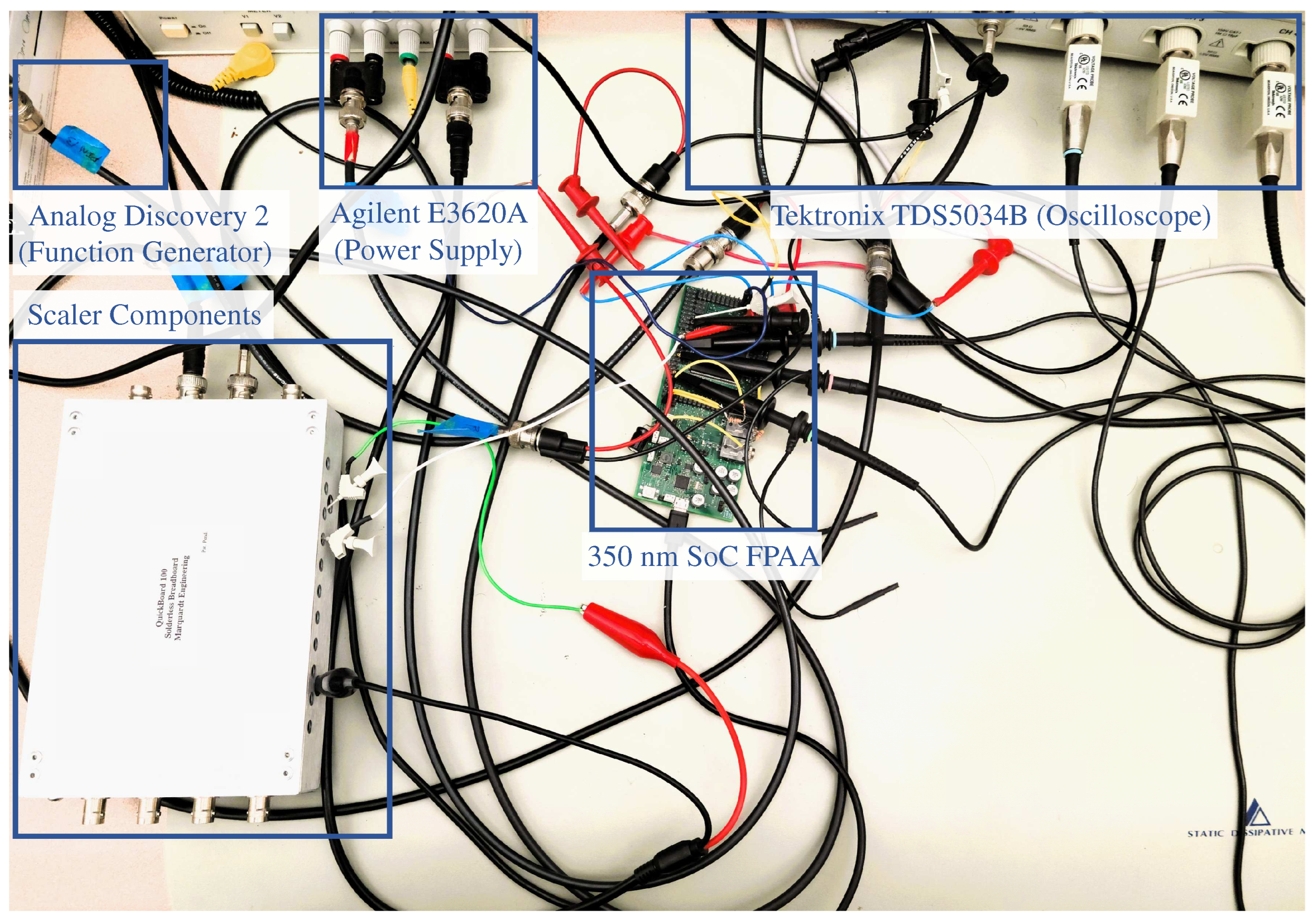
As shown in
Figure 4, with the exception of the scaler circuit, we construct all other extrema pulse generator circuits on the 350
SoC FPAA. During characterization, we supply dynamic voltages from a function generator (Digilent Analog Discovery 2), supply static voltages from a power supply (Agilent E3620A), and acquire extrema samples from an 8-bit oscilloscope (Tektronix TDS5034B) on the falling edge of
. An annotated photograph of our experimental test setup is shown in
Figure 9. We optimize and demonstrate our circuit first for a quadratic chirp and then for an ECG signal. The majority of the power draw of the extrema pulse generator stems from use of OTA circuits. The OTA-capacitor interactions on each OTA output node determine the bandwidth of the overall extrema pulse generator. Since the OTAs are biased in subthreshold saturation, the transconductance of each OTA scales proportionally to its bias current. Consequently, the overall power scales proportionally to the input bandwidth. In this work, the power-bandwidth scaling factor is 100
/
, which translates to a
draw for the quadratic chirp and a
draw for the ECG.
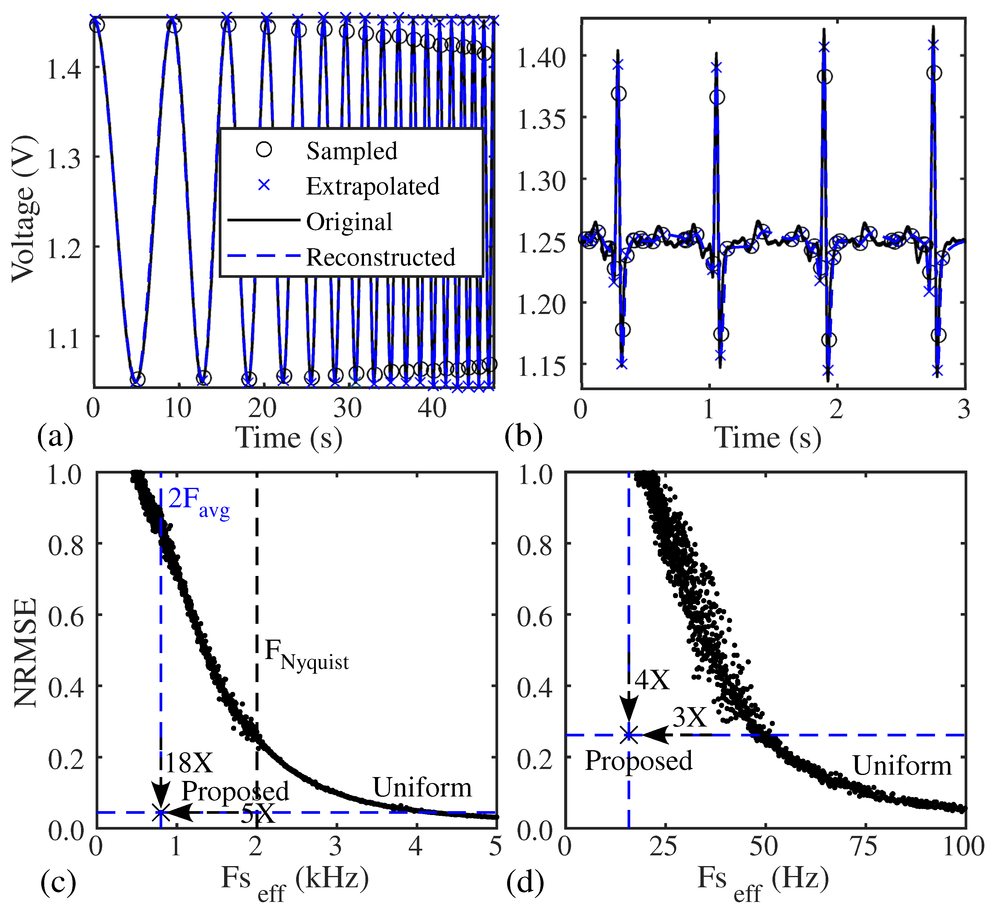
From the reconstructed waveforms in
Figure 10a,b, we visually observe that the ECG and the quadratic chirp can be reconstructed quite well. Numerically, the NRMSE corresponding to the reconstructions shown in
Figure 10a,b are 0.044 (quadratic chirp) and 0.261 (ECG). These NRMSEs are substantially less than the NRMSEs observed if these same signals are uniformly sampled at the same mean rate. Typically, uniform sampling would need to sample a couple of times faster than our proposed nonuniform sampling approach in order to achieve a similar reconstruction error. In a quadratic chirp, the average signal frequency (
) is less than a quarter of the global Nyquist rate of the signal. We therefore experimentally find that extrema sampling, which samples at a rate of roughly
, results in an effective sampling rate of roughly
; even after accounting for the sampling of timestamps, extrema sampling reduces the amount of data recorded during the acquisition of a quadratic chirp while achieving an 18-fold lower reconstruction error than uniform sampling. If uniform sampling is used, the ECG signal must be sampled three times faster on average in order to obtain the NRMSE as the extrema sampling approach. Furthermore, the NRMSE in uniform sampling is four-fold higher given the same
as the extrema sampling approach. In both ECG and quadratic chirp sampling, extrema sampling remains a Pareto improvement over uniform sampling, which means that it is an improvement in both NRMSE and
compared to the Pareto front of the uniform sampling approach (even after accounting for any additional overhead associated with timestamp acquisition). Nevertheless, implementation nonidealities (mostly false positives), mean that solutions lying on the ideal Pareto front in
Figure 2c cannot be attained with our extrema pulse generator.
We compare the performance of previous nonuniform sampling methodologies; specifically, audio-range FPAA or application-specific integrated circuit (ASIC) approaches in similar technology nodes are compared with our extrema pulse generator in
Table 1. Notably, reference [
39] is a recent demonstration of extrema sampling for a task other than data rate reduction [
39];the authors use maxima sampling for envelope signal estimation in a resource-constrained voltage-controlled oscillator (VCO) with automatic gain control. We find that the proposed extrema pulse generator is more energy-efficient than other nonuniform sampling methodologies on FPAAs [
17,
18,
27], drawing less power for the same input bandwidth. A better performance can be attained on ASICs [
25] since routing parasitics can be made lower than an FPAA implementation.
As demonstrated, PCHIP reconstruction works well; however, our PCHIPs do not leverage information pertaining to the classification of the sample points (maximum, minimum, or false positive) explicitly. In subsequent discussions, the performance can be improved further by extracting information from sample point classification. The extrema pulse generator also has a tradeoff between noise immunity and output delay, which should be decoupled in future architectural designs. Nevertheless, the great potential of extrema sampling for data reduction in ADCs is clearly demonstrated by the results of this work.


