Communication

Design of Impedance Matching Network for Low-Power, Ultra-Wideband Applications

Department of Electrical and Computer Engineering, McMaster University, Hamilton, ON L8S 4L8, Canada
*
Author to whom correspondence should be addressed.
J. Low Power Electron. Appl. 2024, 14(1), 16; https://doi.org/10.3390/jlpea14010016
Submission received: 29 January 2024 / Revised: 14 March 2024 / Accepted: 16 March 2024 / Published: 19 March 2024

Abstract

:
This paper addresses the design of ultra-wideband (UWB) impedance matching networks operating in the unlicensed 3.1–10.6 GHz frequency band for low-power applications. It improves the simplified real frequency technique (SRFT) by adding a realizability check and employing an iterative approach with different initial guesses in optimization to achieve realizable solutions under the requirements of UWB, low-power consumption, and a minimum number of circuit components. The comparison of solutions obtained using the SRFT with published solutions based on the Chebyshev filter theory is presented. It is shown that the optimal SRFT solution requires fewer components in the impedance matching network, maximizes the RF power delivery over the UWB spectrum with a reflection coefficient below −10 dB, and allows for circuit optimization to reduce power consumption. Using the improved SRFT, it demonstrates a systematic approach to find the strategies and limitations of designing the input matching networks for low-power UWB applications using GlobalFoundries 90 nm BiCMOS technology.

1. Introduction

Ultra-wideband (UWB) technology is characterized by exceptional features, such as high data rate, low power spectral density, enhanced target recognition, precise localization, and ranging capabilities [1]. These qualities make UWB a desirable choice for a wide variety of applications, including wireless communication, radar, and imaging. In these applications, the primary focus is ensuring the optimal transmission and reception of signals within the operational bandwidth. Hence, the design of broadband impedance matching networks (IMN) has emerged as a significant area of interest for engineers [2].
To match a source impedance ZS to an arbitrary load impedance ZL, as illustrated in Figure 1, various theories and techniques have been developed. To meet this objective, Fano [3] and Youla [4] invoked the gain-bandwidth limitation theory and utilized the Darlington representation, where the load ZL is represented by a lossless two-port terminated in a unit resistor. Analytical models for determining the IMN are also used, but they require an analytical model of the load impedance [5] and often result in suboptimal solutions in terms of circuit performance metrics and network complexity [6].
Another approach to the design of passive IMNs relies on filter theory [7,8,9,10]. The approach employs either a cascaded L-section topology consisting of high-pass and low-pass filters [7,8] or a bandpass filter [9,10]. These fixed topologies, however, may not necessarily provide a minimum number of elements in the IMN for a specific load [6]. A related approach employs series or tank resonators, and it is based on manipulations of the resonant frequencies [11,12]. When these resonant frequencies can be strategically spaced apart while maintaining an acceptable gain variation, it is possible to attain a broadband IMN. However, it may not prove effective for high fractional bandwidth (FBW) requirements, where many resonators are required.
Design approaches for IMNs with no prior assumption about the network topology, no need for analytical load modelling, and leading to a minimum element count have always been desired. To fulfill this need, Carlin [5] developed the so-called real frequency technique (RFT) utilizing the real-frequency (e.g., experimental) load-impedance data along with numerical optimization. The initial version of the RFT technique was to solve a single matching problem, i.e., a complex load impedance ZL with a source impedance Zs = 50 Ω [5]. The subsequently developed RFTs can be classified into four distinct categories, namely the line segment technique (RFT-LST), the direct computational technique (DCT), the parametric approach, and the simplified real frequency technique (SRFT) [2]. The line segment technique, direct computational technique, and parametric approach formulate the objective function utilizing the unknown input immittance (driving point admittance or impedance) across the entire angular real-frequency ω axis. The procedure starts with the real part of the input immittance, as the imaginary part would be found with the Hilbert transformation or the Gewertz procedure. A lossless two-port IMN can be synthesized by finding an optimized input immittance. The line segment technique formulates the real part of the input immittance as a linear combination of straight lines R in = k = 1 N a k ( ω ) R k [5]. On the other hand, the direct computational technique defines the real part of a positive real minimum immittance as a rational even function R in ( ω ) = E v { Z in ( s ) } | s = j ω = N ( ω 2 ) D ( ω 2 ) [13]. The parametric approach represents this rational function in a parametric form Z in ( s ) = k = 1 N A k s + s k and takes the even function of Zin as the real part of Zin [14]. Finally, the simplified real frequency technique simplifies the task by defining the two-port scattering parameters of an IMN as rational functions [15], which helps in handling the double-matching problems [13,16] and streamlining the computation process [17].
In this paper, we present the simplified real frequency technique in detail in Section 2 and apply this technique to the design of the IMN for low-power applications in Section 3, followed by the conclusions.

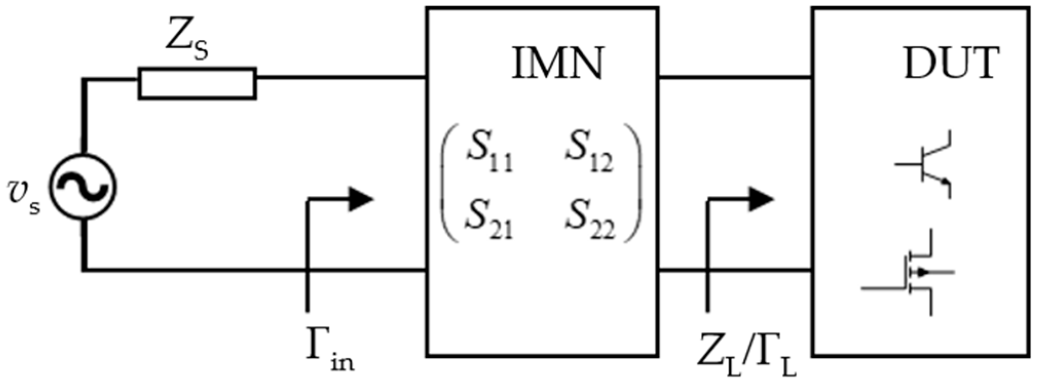
2. Simplified Real Frequency Technique (SRFT)

The SRFT starts with defining the scattering parameters, SIMN, of an IMN containing lossless reciprocal passive elements based on three polynomials: h, g, and f. Because the IMN should satisfy the paraunitary requirement S IMN S IMN = I [17,18,19], where I is the identity matrix, SIMN is expressed as
S IMN = [ S 11 = h ( s ) g ( s ) S 12 = f ( s ) g ( s ) S 21 = f ( s ) g ( s ) S 22 = ( 1 ) k h ( s ) g ( s ) ]
where h(s) and g(s) are polynomials of order n, n is the number of elements in an IMN, and k = 0, 1, 2, …, n. The polynomial g(s) is strictly Hurwitz, which has all poles on the left-hand side of the complex plane to avoid impractical or unrealizable solutions. The polynomial f(s) provides the information about the transmission zeros of the IMN. Transmission zeroes are defined as the frequencies at which the output signal is completely cut off. In consideration of a transmittance function S21 that may possess finite zeros at ±i, zeros at infinity, or zeros at the origin, its general form is expressed as
f ( s ) = s k i = 1 m ( s 2 + ω i 2 )
Such form implies that f(s) can be either an odd function or an even function. The presence of finite zeros, such as in the modified Chebyshev design [20], often increases the number of elements and complicated synthesis [21]. Therefore, it is preferable for f(s) to be in the s k form. The parameter k may assume a value of zero in low-pass scenarios and a value greater than one in bandpass and high-pass cases [22]. The lossless condition introduces a relationship among the polynomials f, g, and h. Knowing f(s) allows for expressing g(s) as a function of h(s) as
g ( s ) g ( s ) = h ( s ) h ( s ) + f ( s ) ( s )
The objective in designing the IMN for a known load can be achieved by either maximizing the transductor power gain GT, ideally approaching unity, or minimizing the reflection coefficient Γin, as follows from
G T = | S 21 | ( 1 | Γ L | 2 ) | 1 S 22 Γ L | 2
and
Γ in = S 11 + S 21 S 12 Γ L 1 S 22 Γ L
The SRFT utilizes optimization techniques to determine the optimal polynomial h(s) and, consequently, the corresponding polynomial g(s). Optimization aims to minimize the error function based on the objective function (4) or (5) for load impedance data.

3. Results and Discussion

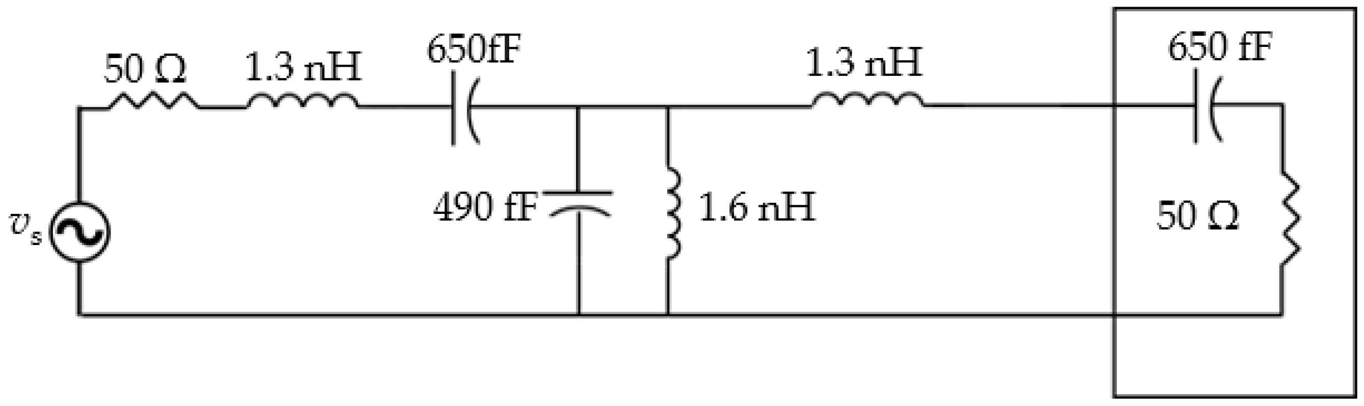
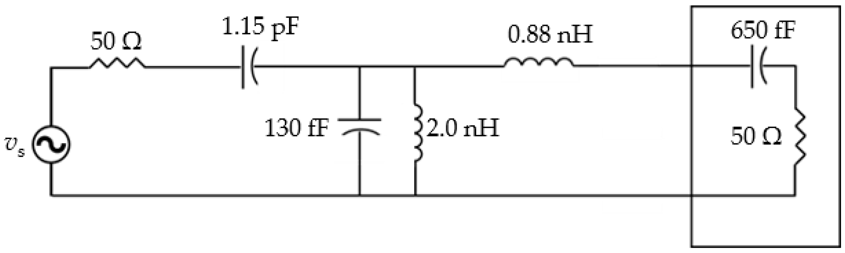
3.1. Comparing SRFT and Chebyshev Filter-Based Solutions

Bode and Fano demonstrated a physical limitation on the maximum achievable bandwidth for loads comprising resistors and reactive elements [3,23]. For example, in the case of a load with a resistor R and capacitor C connected in series, this limitation can be found by [24]
0 1 ω 2 ln [ 1 | Γ in ( ω ) | ] d ω < π R C
It is evident from (6) that efficient broadband impedance-matching structures inherently exhibit filter-like characteristics [23,24]. For optimal matching performance, all reflection coefficients |Γin(ω)| within the frequency band of interest are preferred to be small while |Γin(ω)| outside this frequency range are one (i.e., perfect reflection). So, the sharper the cut-off rate of the filter is, the better the performance of the IMN will be [25]. It is well known that the Chebyshev filter offers a sharper cut-off; therefore, it is chosen for comparison with the SRFT method. In [9], a UWB Chebyshev filter theory was used to design the IMN for a load modelled by a 50 Ω resistor in series with a 650 fF capacitor. The IMN comprises five components, with their values (from [9]) depicted in Figure 2. The reflection coefficient resulting from this design is shown in Figure 3, obtained by simulating the circuit in Figure 2 using the Cadence Virtuoso Spectre circuit simulator with ideal elements from the analog library.
On the other hand, when designing a UWB IMN using SRFT, the choice of the optimization method plays a significant role in obtaining a solution with better performance. Most reported RFT and SRFT techniques use Levenberg–Marquart optimization [15,17,26], a local optimization algorithm that aims to find the minimum of a function in the vicinity of an initial guess. Thus, it is best suited for problems where a solution is expected to be found in the proximity of the initial guess [27]. Selecting a good initial guess in such a highly nonlinear optimization process is critical, and it substantially impacts the ability to reach the optimal IMN [15,22,28].
To see if we can obtain a better solution than the Chebyshev filter approach, we applied the SRFT to the same load as in [9]. It is observed that the SRFT may yield solutions that cannot be realized by LC elements, even if they demonstrate superior matching performance. We characterize them as unrealizable solutions. One such solution is shown by the red symbols in Figure 3. The realizability of a solution can be verified by examining the input reflection coefficients observed at the input port of the IMN when its output port is terminated with either a short or an open circuit. For example, when the IMN comprises solely reactive elements, and when the output port is open-circuited, its input reflection coefficient Γin,OC or input impedance Zin,OC can be expressed in terms of f(s), h(s), and g(s) as
Γ in , OC ( s ) = S 11 ( s ) + S 12 2 ( s ) 1 S 22 ( s ) = h ( s ) [ g ( s ) + ( 1 ) k h ( s ) ] + f 2 ( s ) g ( s ) [ g ( s ) + ( 1 ) k h ( s ) ] = N ( s ) D ( s )
and
Z in , OC ( s ) = 1 + Γ in , OC ( s ) 1 Γ in , OC ( s ) = D ( s ) + N ( s ) D ( s ) N ( s )                  = k n s n + k n 1 s n 1 + k 1 s + k 0 + k p 0 s + k p 1 s j ω p 1 + k p 1 s + j ω p 1
where N(s) and D(s) are the numerator and denominator of the input reflection coefficient. In (8), the input impedance Zin,OC is expressed in a partial-fraction form, where ki is the coefficient of si, kpi and k p i are residues, and ωpi are poles. Since the input impedance Zin,OC only comprises reactive components, it should exhibit the following three characteristics. First, it must be an odd function (k0 = 0) with the numerator and denominator differing by one degree. Second, it should contain only simple zeros and poles, all interlaced on the axis. Third, the residues of Zin,OC for all poles must be real-positive [29]. If a solution violates any of these features, it cannot be implemented only by reactive elements. For instance, the red curve in Figure 3 is not realizable because of its k0 < 0.
To find a realizable solution, an exhaustive search with various initial guesses using the Levenberg–Marquardt optimization method is required. In the SRFT, it assigns initial-guess values to the n + 1 coefficients of h(s). Each coefficient value is randomly selected from a continuous uniform distribution within the bounds defined by lb and ub for quick optimization convergence [30]. If the solution fails to satisfy the feasibility conditions outlined above, another initial guess is used until a realizable solution is found. Based on this iterative approach, a solution with a maximum reflection coefficient of −13.7 dB in the whole UWB spectrum has been found, as shown by the green symbols in Figure 3. This solution is better than the solution obtained using the Chebyshev filter theory, which features a maximum reflection coefficient of −12.3 dB [9]. Moreover, the solution obtained using the SRFT requires only four elements, as demonstrated in Figure 4, as opposed to the five elements required by the Chebyshev design. This is beneficial, particularly in this example, saving space since an inductor is eliminated.
Another way to verify the performance of an IMN solution for a particular load is to check how close it is to the Bode–Fano limit, πRC in (6). As |Γin(ω)| in (6) cannot be determined using an analytical expression in SRFT, it is assumed that |Γin(ω)| remains constant and equal to an average value Γavg across the specified frequency band. This approximation can simplify (6) as [24]
B W ω 0 2 ln ( 1 Γ avg ) < π R C
where B W = ω max ω min , ω 0 = ω max ω min , and ω min and ω max are the lower and upper limits of the frequency band. For the realizable solution shown in Figure 3, the averaged reflection coefficient Γavg is 0.115. This results in 78 ps, closer to the Bode–Fano limit of 102 ps compared with the 72 ps value obtained from [9].
As an alternative, one may consider utilizing global optimization techniques. These methods can offer the lowest possible reflection coefficient at the expense of significantly longer computations. RFT-based techniques predominantly employ local minimum optimization methods, yielding a solution quickly. As exemplified above, SRFT may result in an unrealizable solution, in which case another search must be initiated. With a global optimization method, e.g., the genetic algorithm (GA), the algorithm may bypass a realizable solution and converge to an unrealizable solution due to its inclination towards achieving the lowest minimax objective. Indeed, [31] reports an approach using the GA; however, impractical responses are sometimes obtained. It is clear that synthesizing a realizable solution for a UWB IMN (topology and component values) is problematic. While the optimization may indicate the existence of a solution, it may be difficult or even impossible to synthesize a practical network, particularly in scenarios involving intricate configurations and components like transformers. As shown in [32], some preassumption is required to find the right synthesis.

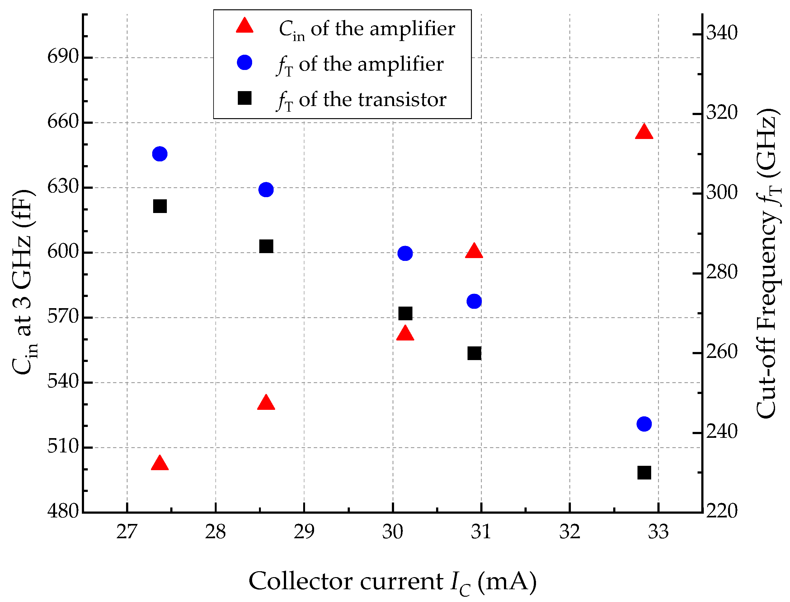
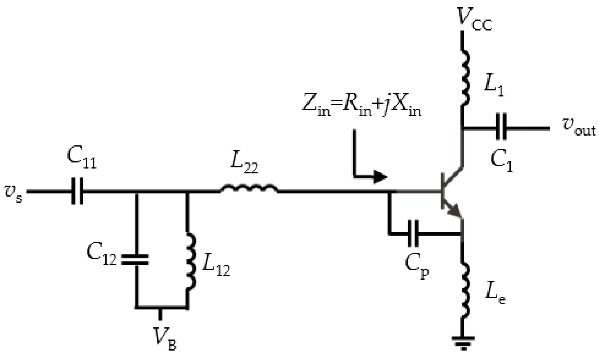
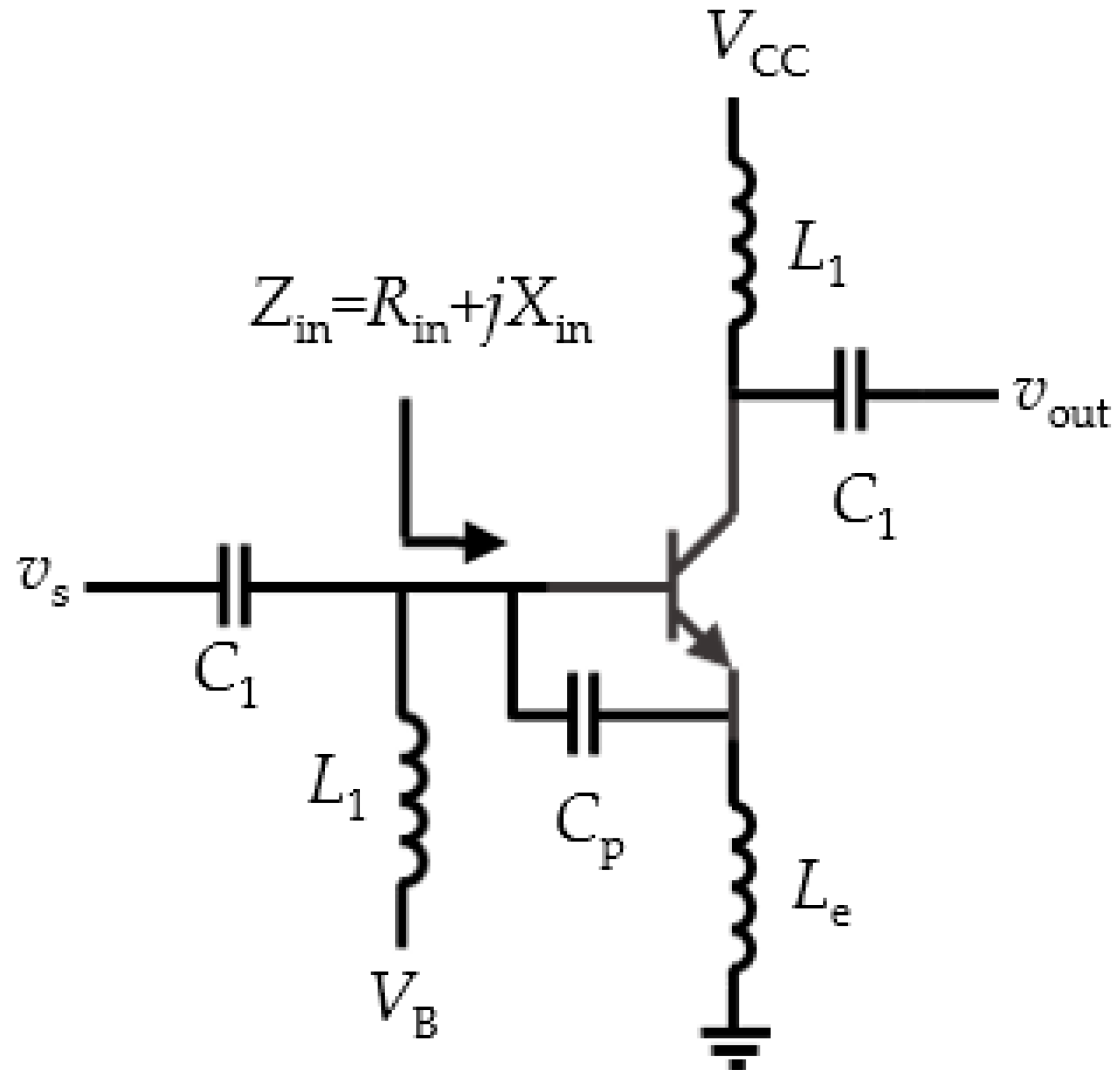
3.2. IMN for Low-Power Applications

Assuming the antenna provides a source impedance ZS = 50 Ω in the frequency band of interest, the improved SRFT can find an IMN to match a load ZL to the 50 Ω source impedance, as shown in Figure 1. The inductor-degenerated topology is a commonly used technique [33] for amplifiers using bipolar junction transistors (BJT) [34] and field-effect transistors (FET) [35]. Figure 5 shows the frequently used common emitter amplifier with a degeneration inductor Le to obtain the required input resistance for narrowband [34] and wideband matching [10]. Here, C1 serves as a DC blocking capacitor, and L1 is an RF choke to isolate the biasing circuit from the RF port. We demonstrate the designs of the input matching networks based on the improved SRFT for different bias conditions and circuit topologies using GlobalFoundries 90 nm BiCMOS technology.
For low-power applications, the circuit’s input reactance sets the lower power consumption limit. When we reduce the power consumption by decreasing the base-to-emitter voltage applied to the BJT, the base-emitter junction capacitor (Cbe) becomes smaller, resulting in a smaller Cin (or a bigger absolute value of input reactance) and a lower Bode–Fano limit, which makes it more challenging to find an IMN solution with Γin < −10 dB. To examine the lowest power consumption for the inductive degeneration topology shown in Figure 5 and ensure the circuit has sufficiently high cut-off frequency fT to cover the 3.1–10.6 GHz band, Figure 6 shows the equivalent Cin at 3 GHz, the fT of the transistor, and the fT of the amplifier (with Le in the range of 30–40 pH) at different collector currents IC. The transistor used in the simulation has a length and width of 90 nm and 10 μm, respectively, and its collector is biased at 1.0 V. To be able to compare with the result in [9] and ensure that we can obtain a realizable IMN solution with Γin < −10 dB over 3.1–10.6 GHz, we start with the collector current IC = 32.8 mA, at which Cin is about 650 fF, which is the same as the value reported in [9]. As expected, the reduction in the collector current decreases the equivalent input capacitance Cin at 3 GHz due to the reduction in Cbe. The lowest collector current for a realizable IMN solution is at IC = 27.4 mA. Further reducing Cin is prohibited by the Bode–Fano limit in (9). The Rin of this circuit exhibits frequency-dependent variations due to the inherent characteristics of the BJT transistor in this technology. The intrinsic base resistance varies from approximately 50 Ω to 17 Ω across the frequency band of interest. The adjustment of this variation around 50 Ω with the assistance of Le poses an additional challenge in the quest for an IMN compared to a circuit that provides a constant 50 Ω over the bandwidth. In addition, comparing the circuit’s cut-off frequency (fT) and the transistor’s fT at these bias points indicates that the emitter degeneration inductor Le enhances the fT of the circuit slightly and follows the fT of the transistor.
To further reduce the power consumption, Cin is to be established by adding a capacitor Cp in parallel at the amplifier input, as shown in Figure 7. Incorporating Cp mitigates variations in Rin with respect to frequency as it is placed in parallel with the intrinsic impedance of the transistor. This arrangement brings Rin closer to 50 Ω. When reducing the collector current IC, we adhere to two essential criteria: (1) ensuring that the IMN remains below −10 dB across the bandwidth and (2) maintaining the circuit’s fT above 100 GHz to ensure a circuit bandwidth up to 10.6 GHz. Cp and Le are adjusted to ensure that Zin and fT meet these requirements. Figure 8 shows the equivalent Cin at 3 GHz, the cut-off frequencies fT of the transistor and the amplifier (with Le in the range of 60–140 pH) at different collector currents IC. It is observed that, although adding Cp decreases the fT of the amplifier, we can further reduce the collector current IC to 6.1 mA. When comparing with the initial IC = 32.8 mA, we observe an 81.3% reduction in collector current while maintaining the fT at around 100 GHz to ensure the amplifier operates at 10.6 GHz. A further decrease in the collector current IC would yield a circuit with a reduced fT or Γin surpassing −10 dB. Table 1 shows the component values of the IMN, Cp, and Le for the bias conditions of the base-to-emitter voltage VBE and the collector current IC in Figure 8.
Based on the amplifier shown in Figure 7, Figure 9 shows the complete amplifier design with its input IMN. Table 1 shows the component values of the circuit for the bias conditions in Figure 8. The ICmax and ICmin specify the tolerable range of the collector current to which the IMN solution can still maintain Γin < −10 dB over 3.1–10.6 GHz. Maintaining the tolerance for ICmin at low bias currents is challenging because Cin and the resulting Bode–Fano limit reduce, and, therefore, it is hard to find a solution with Γin < −10 dB.

4. Conclusions

We demonstrated that the SRFT is a highly efficient design method for UWB IMNs, which provides solutions with the minimum component count in the IMN. On the other hand, we also show that not all optimal reflection-coefficient responses obtained with the SRFT can be assured to be realizable or synthesizable. The choice of the optimization method and the initial guess are essential for uncovering solutions in RFT-based methodologies. With local optimization, which is usually employed by the SRFT methods, an improper initial point can result in a solution that is optimal in a mathematical sense but is physically unrealizable with components such as capacitors and inductors. On the other hand, local optimization methods converge fast, thus allowing for exhaustive searches with various initial points. Such searches are not feasible with global optimization methods, which are slower and more difficult to steer through an initial guess and converge to a realizable solution. Nonetheless, there exists an opportunity for further investigation to rigorously define the underlying SRFT model features leading to unrealizable solutions, thereby providing guidelines for the selection of the initial guess as well as the formulation of constraints to steer the optimization away from such solutions. Finally, we have demonstrated that the improved SRFT ensures realizable IMN solutions. The systematic approach in this paper enables us to find a UWB IMN solution with an 81.3% power reduction and an amplifier fT at around 100 GHz to ensure the amplifier operates at 10.6 GHz.

Author Contributions

Conceptualization, S.H. and C.-H.C.; methodology, S.H. and C.-H.C.; software, S.H.; validation, S.H., C.-H.C. and N.K.N.; formal analysis, S.H.; investigation, S.H. and C.-H.C.; writing—original draft preparation, S.H.; writing—review and editing, S.H., C.-H.C. and N.K.N.; visualization, S.H. and C.-H.C.; supervision, C.-H.C. and N.K.N.; funding acquisition, C.-H.C. and N.K.N. All authors have read and agreed to the published version of the manuscript.

Funding

This research was funded by Natural Sciences and Engineering Research Council: RTI-2020-00456, RGPIN-2017-06058, RGPIN-2020-05706.

Data Availability Statement

Data is contained within the article.

Conflicts of Interest

The authors declare no conflict of interest.

References

  1. Fontana, R.J. Recent system applications of short-pulse ultra-wideband (UWB) technology. IEEE Trans. Microw. Theory Tech. 2004, 52, 2087–2104. [Google Scholar] [CrossRef]
  2. Yarman, B.S. Real frequency techniques a historical review. In Design of Ultra Wideband Antenna Matching Networks; Yarman, B.S., Ed.; Springer Science + Business Media B. V.: Dordrecht, The Netherlands, 2008; pp. 1–8. [Google Scholar]
  3. Fano, F.M. Theoretical limitations on the broadband matching of arbitrary impedances. J. Frankl. Inst. 1950, 249, 57–83. [Google Scholar] [CrossRef]
  4. Youla, D.C. A new theory of broadband matching. IEEE Trans. Circuit Theory 1964, 11, 30–50. [Google Scholar] [CrossRef]
  5. Carlin, H.J. A new approach to gain-bandwidth problems. IEEE Trans. Circuits Syst. 1977, 24, 170–175. [Google Scholar] [CrossRef]
  6. Carlin, H.J.; Amstutz, P. On optimum broadband matching. IEEE Trans. Circuits Syst. 1981, 28, 401–405. [Google Scholar] [CrossRef]
  7. Breed, G. Improving the Bandwidth of Simple Matching Networks; Summit Technical Media, LLC: Bedford, NH, USA, 2008; pp. 56–60. [Google Scholar]
  8. Yang, H.; Kim, K. Ultra-wideband impedance matching technique for resistively loaded vee dipole antenna. IEEE Trans. Antennas Propagat. 2013, 66, 5788–5792. [Google Scholar] [CrossRef]
  9. Bevilacqua, A.; Niknejad, A.M. An ultrawideband CMOS low-noise amplifier for 3.1–10.6-GHz wireless receivers. IEEE J. Solid-State Circuits 2004, 39, 2259–2268. [Google Scholar] [CrossRef]
  10. Ismail, A.; Abidi, A.A. A 3–10-GHz low-noise amplifier with wideband LC-ladder matching network. IEEE J. Solid-State Circuits 2004, 39, 2269–2277. [Google Scholar] [CrossRef]
  11. Zhao, C.; Duan, D.; Xiong, Y.; Liu, H.; Yu, Y.; Wu, Y.; Kang, K. A K-/Ka-band broadband low-noise amplifier based on the multiple resonant frequency technique. IEEE Trans. Circuits Syst. I 2022, 69, 3202–3211. [Google Scholar] [CrossRef]
  12. Zailer, E.; Belostotski, L.; Plume, R. Wideband LNA noise matching. IEEE J. Solid-State Circuits Lett. 2020, 3, 62–65. [Google Scholar] [CrossRef]
  13. Carlin, H.J.; Yarman, B.S. The double matching problem: Analytic and real frequency solutions. IEEE Trans. Circuits Syst. 1983, 30, 15–28. [Google Scholar] [CrossRef]
  14. Fettweis, A. Parametric representation of Brune functions. Int. J. Circuit Theory Appl. 1979, 7, 113–119. [Google Scholar] [CrossRef]
  15. Yarman, B.S.; Carlin, H.J. A simplified “real frequency” technique applied to broad-band multistage microwave amplifiers. IEEE Trans. Microw. Theory Tech. 1982, 30, 2216–2222. [Google Scholar] [CrossRef]
  16. Carlin, H.J.; Civalleri, P. On flat gain with frequency-dependent terminations. IEEE Trans. Circuits Syst. 1985, 32, 827–839. [Google Scholar] [CrossRef]
  17. Jarry, P.; Beneat, J.N. Microwave Amplifier and Active Circuit Design Using the Real Frequency Technique; John Wiley & Sons, Inc.: Hoboken, NJ, USA, 2016. [Google Scholar]
  18. Wu, D.Y.-T.; Mkadem, F.; Boumaiza, S. Design of a Broadband and Highly Efficient 45W GaN Power Amplifier via Simplified Real Frequency Technique. In Proceedings of the IEEE MTT-S International Microwave Symposium, Anaheim, CA, USA, 23–28 May 2010. [Google Scholar]
  19. Carlin, H.J. The scattering matrix in network theory. IRE Trans. Circuit Theory 1956, 3, 88–97. [Google Scholar] [CrossRef]
  20. Limand, J.S.; Park, D.C. A modified Chebyshev bandpass filter with attenuation poles in the stopband. IEEE Trans. Microw. Theory Tech. 1997, 45, 898–904. [Google Scholar]
  21. Yeung, L.K.; Wu, K.-L. A compact second-order LTCC bandpass filter with two finite transmission zeros. IEEE Trans. Microw. Theory Tech. 2003, 51, 337–341. [Google Scholar] [CrossRef]
  22. Yarman, B.S.; Fettweis, A. Computer-aided double matching via parametric representation of Brune functions. IEEE Trans. CAS 1990, 37, 212–222. [Google Scholar] [CrossRef]
  23. Bode, H.W. Network Analysis and Feedback Amplifier Design; D. Van Nostrand Co., Ltd.: New York, NY, USA, 1945; pp. 350–371. [Google Scholar]
  24. Steer, M. Microwave and RF Design Networks, 3rd ed.; NC State University: Raleigh, NC, USA, 2019. [Google Scholar]
  25. Matthaei, G.; Young, L.; Jones, E.M.T. Microwaves Filters, Impedance-Matching Networks, and Coupling Structures; McGraw-Hill: New York, NY, USA, 1985. [Google Scholar]
  26. Dai, Z.; He, S.; You, F.; Peng, J.; Chen, P.; Dong, L. A new distributed parameter broadband matching method for power amplifier via real frequency technique. IEEE Trans. Microw. Theory Tech. 2015, 63, 449–458. [Google Scholar] [CrossRef]
  27. Lera, G.; Pinzolas, M. Neighborhood based Levenberg–Marquardt algorithm for neural network training. IEEE Trans. Neural Netw. 2002, 13, 1200–1203. [Google Scholar] [CrossRef]
  28. Sengül, M. Design of practical broadband matching networks with lumped elements. IEEE Trans. Circuits Syst. II 2013, 60, 552–556. [Google Scholar] [CrossRef]
  29. Temes, G.C.; Lapatra, J.W. Introduction to Circuit Synthesis and Design; McGraw-Hill: New York, NY, USA, 1977. [Google Scholar]
  30. Köprü, R. FSRFT—Fast simplified real frequency technique via selective target data approach for broadband double matching. IEEE Trans. Circuits Syst. II Express Briefs 2017, 64, 141–145. [Google Scholar]
  31. Yegin, K.; Martin, A.Q. On the design of broadband loaded wire antennas using the simplified real frequency technique and a genetic algorithm. IEEE Trans. Antennas Propagat. 2003, 51, 220–228. [Google Scholar] [CrossRef]
  32. Gerkis, A.N. Broadband impedance matching using the real frequency network synthesis technique. Appl. Microw. Wirel. 1998, 10, 26–36. [Google Scholar]
  33. Bellomo, A.F. Gain and noise considerations in RF feedback amplifier. IEEE J. Solid-State Circuits 1968, 3, 290–294. [Google Scholar] [CrossRef]
  34. Meyer, R.G.; Mack, W.D. A 1-GHz BiCMOS RF front-end IC. IEEE J. Solid-State Circuits 1994, 29, 350–355. [Google Scholar] [CrossRef]
  35. Shaeffer, D.K.; Lee, T.H. A 1.5-V, 1.5-GHz CMOS low noise amplifier. IEEE J. Solid-State Circuits 1997, 32, 745–759. [Google Scholar] [CrossRef]
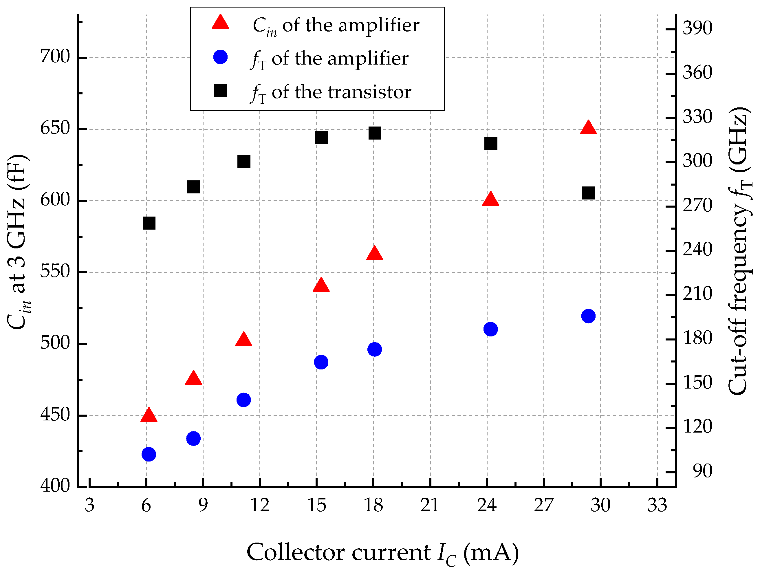
Figure 1. Matching an arbitrary load impedance ZL to a source impedance ZS.
Jlpea 14 00016 g001
Figure 2. UWB IMN based on the Chebyshev filter theory in [9].
Jlpea 14 00016 g002
Figure 3. Reflection coefficient of the design using the Chebyshev filter theory (●) [9], the SRFT-based realizable solution (▲), and the SRFT-based unrealizable solution (■). The maximum Γin of each response is indicated by the blue color symbols.
Jlpea 14 00016 g003
Figure 4. UWB IMN based on the SRFT.
Jlpea 14 00016 g004
Figure 5. Inductively degenerated common-emitter amplifier.
Jlpea 14 00016 g005
Figure 6. The equivalent input capacitance Cin (▲) at 3 GHz and the fT (●) of the inductive degeneration common-emitter amplifier in Figure 5 with Le in the range of 30–40 pH and the fT (■) of the transistor at different collector currents IC. The transistor used in the simulation has a length and width of 90 nm and 10 μm, respectively, and its collector is biased at VCC = 1.0 V.
Jlpea 14 00016 g006
Figure 7. An inductively degenerated common-emitter amplifier with a capacitor Cp connected in parallel to the input of the amplifier.
Jlpea 14 00016 g007
Figure 8. The equivalent input capacitance Cin (▲) at 3 GHz and the fT (●) of the inductive degeneration common-emitter amplifier with CP and Le in Figure 7 and the fT (■) of the transistor at different collector currents IC. The transistor used in the simulation has a length and width of 90 nm and 10 μm, respectively, and its collector is biased at VCC = 1.0 V.
Jlpea 14 00016 g008
Figure 9. Inductively degenerated common-emitter amplifier with its UWB IMN.
Jlpea 14 00016 g009
Table 1. Component values for the amplifier in Figure 9 with VCC = 1.0 V.
Cin (fF)655600562540502475449
Parameter
  VB (mV)923910894886873863852
  IC (mA)29.324.218.015.211.18.56.1
  Le (pH)6060758090110140
  Cp (fF)100140180195210220230
  C11 (pF)1.010.920.920.870.930.790.79
  L12 (nH)2.092.22.232.172.182.252.56
  C12 (fF)18011115813414011661
  L22 (nH)1.020.911.151.111.171.251.21
  ICmin (mA)2521.4615.913.4210.858.56.1
  ICmax (mA)34.530.524.222.717.710.811.4
Disclaimer/Publisher’s Note: The statements, opinions and data contained in all publications are solely those of the individual author(s) and contributor(s) and not of MDPI and/or the editor(s). MDPI and/or the editor(s) disclaim responsibility for any injury to people or property resulting from any ideas, methods, instructions or products referred to in the content.

