Article

A Simplified GmC Filter Technique for Reference Spur Reduction in Phase-Locked Loop

by
P. Purushothama Chary
*,
Rizwan Shaik Peerla
and
Ashudeb Dutta
Department of Electrical Engineering, Indian Institute of Technology, Hyderabad 502285, India
*
Author to whom correspondence should be addressed.
J. Low Power Electron. Appl. 2024, 14(1), 17; https://doi.org/10.3390/jlpea14010017
Submission received: 2 February 2024 / Revised: 8 March 2024 / Accepted: 10 March 2024 / Published: 20 March 2024

Abstract

:
This paper presents a wideband approach for L5 and S-band integer-N phase-locked loop (PLL) targeting Indian Regional Navigation Satellite System (IRNSS) applications. A reference spur reduction technique using a G m C filter is proposed. The reference spur is improved by 7 dB when compared with one without any G m C filter. The wideband integer-N PLL is designed and fabricated in UMC 65-nm CMOS process. The G m C filter block consumes 200 μ A current. The wideband voltage-controlled oscillator (VCO) oscillates from 1.6 GHz to 3.2 GHz having a tuning range (TR) of 40 % , achieving a best and worst phase noise of ≈−122 dBc/Hz and ≈ 116 dBc/Hz at a 1 MHz offset, respectively.

1. Introduction

Extreme accuracy is needed for the growing demand for location-based services (LBSs), particularly for space applications or rescue and search operations [1]. To attain the necessary location accuracy, LBSs need either a single global navigation satellite system (GNSS) frequency or several GNSS frequencies [2]. Numerous global navigational systems exist, including GLONASS (Russia), Galileo (EU), and BeiDou (China). A system specifically designed for the Indian subcontinent is the Indian Regional Navigation Satellite System (IRNSS). This system uses navigation signal frequencies between 1.17 GHz to 2.5 GHz. The received signal is weak (≈−130 dB), hence a high-sensitivity receiver is required for proper reception because IRNSS receivers are designed for critical applications like real-time monitoring and precise location positioning. Any receiver’s sensitivity depends on the local oscillator’s (LO) phase noise (PN), spectrum purity, and low spurs [3,4,5,6,7,8,9,10,11,12,13], which makes the design of the phase-locked loop (PLL) complicated [1,14]. In applications of transceivers, it is important to maintain a pure, single-tone spectrum, without unwanted tones to avert a corruption of required data.
This work presents a G m C filtering technique for the reference spur reduction of a wideband PLL. Firstly, a brief overview of PLLs implemented for IRNSS applications is discussed. Then, the reasons and parameters affecting the reference spur generation is presented. After that, the proposed G m C filter technique for reference spur reduction is analyzed. Finally, PLL measurement results and a performance comparison with other latest works are presented and a conclusion of the work is drawn.

1.1. Overview of IRNSS PLL

The L5 and S frequency bands are where the IRNSS receiver typically operates. There are single voltage-controlled oscillator (VCO) [15], multiple VCO PLLs’ [16], and rotatory traveling wave oscillator [17] architectures described in the literature. The most recent research covers both bands with a single broadband voltage-controlled oscillator (VCO) [18]. To achieve this, the PLL must operate at a reasonable power consumption with an acceptable quality factor (Q) and have stability throughout the whole range. In other works, these bands are covered by various PLLs [2]. The feedback divider, which must work over several ranges, is one of the factors contributing to the use of numerous PLLs. A PLL using an extended range divider is presented in [19,20].
Thus, high-performance PLLs mainly require better phase noise and low reference spurs simultaneously. To accomplish this in L5 and S bands, this work provides a wideband integer-N PLL using a single VCO. The wideband PLL covers multiple bands using a single VCO but comes at the cost of extra power to maintain an acceptable inductor’s Q-factor. To maintain PLL stability, the charge pump current ( I C P ) needs to have programmability. The wideband VCO also has a variable VCO gain ( K V C O ), which, along with I C P , affects the reference spur of the PLL.

1.2. Reference Spur in PLL

Ideally in the frequency domain, a PLL should generate a single tone. In reality, this signal is not a single tone because of the unwanted noise added at various points of the PLL, making the spectrum impure. A conventional type-II PLL highlighting the non-idealities causing the reference spur is shown in Figure 1. The phase frequency detector (PFD) senses the error between the reference signal ( F R E F ) and the feedback signal ( F D I V ). A proportional source/sink current is provided by the charge pump (CP), which is converted as a control voltage ( V t u n e ) and passed on to the VCO that generates the output frequency. The feedback divider divides the high-frequency output into a low-frequency signal that is given as input to the PFD.
Non-idealities of the PFD and CP circuits like PFD output mismatch, I C P mismatch, PFD-to-CP propagation delay mismatch, clock feed-through, etc., generate a periodic variation on V t u n e . In the frequency domain, this periodic variation is visualized as signals at F R E F and at its offsets from the VCO output.
Some detailed analyses of spurs due to the above non-idealities are discussed in [21]. The spur level depends on K V C O and on the order of the low-pass filter (LPF). The magnitude of the spur reference is shown in (1) [22] (units are in dBc):
A s p u r = 20 log N · ϕ e · ω L B W ω R E F · 2 20 log ω R E F ω P
where ϕ e is the phase offset due to the leakage current, ω P is the out-of-band pole frequency, ω R E F is the reference frequency, and ω L B W is the loop bandwidth frequency of the PLL as given in (2).
ω L B W I C P · R 1 · K V C O N

1.3. Spur Reduction Techniques
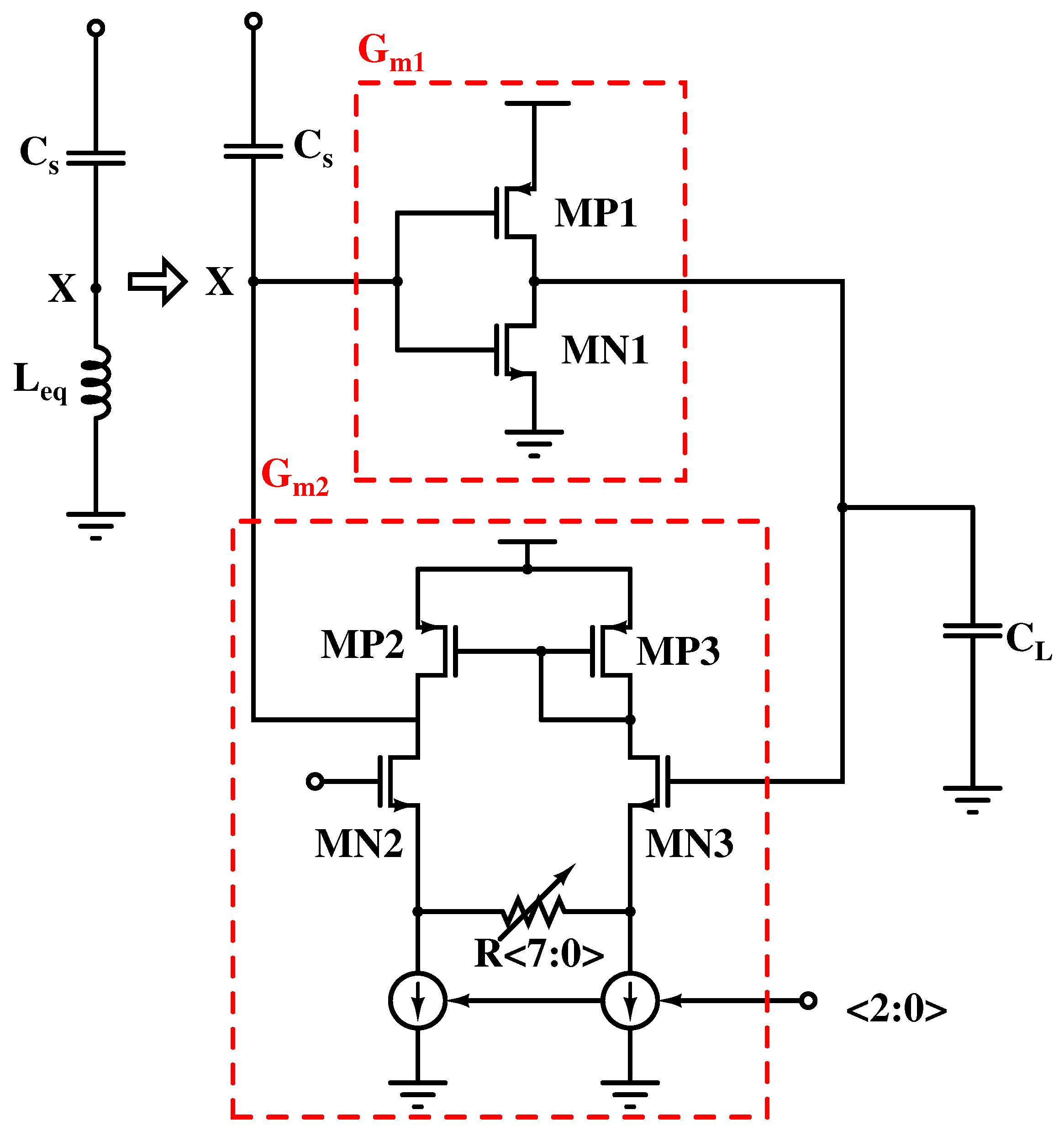
Several methods of spur reduction for PLLs have been published. In [3,4,5,6,7,8,9,10,11,12,13], the authors utilized the higher-order loop filter to achieve an acceptable spur level (< 65 dBc). However, a higher-order loop filter affects the PLL phase margin which might make the system unstable. Figure 2 shows the open-loop gain of a type-II PLL built using second-order and third-order loop filters.
From (1), the reference spur expression for the second- and third-order loop filter is given by (3) and (4), respectively.
A s p u r , 2 n d o r d e r = 20 log N . ϕ e . ω L B W ω R E F . 2 Δ B
A s p u r , 3 r d o r d e r = 20 log N . ϕ e . ω L B W ω R E F . 2 Δ B Δ A
Thus, the spur level is improved by Δ A when the loop filter order is increased from two to three. The amount of spur reduction mainly depends on out-of-band poles, i.e., ω P 1 and ω P 2 . From (1), one can observe that the magnitude of the spur is directly proportional to K V C O and inversely proportional to ω R E F . A lower K V C O has the effect of reducing the total VCO frequency bandwidth. This can be overcome by an additional switched capacitor array (SCA) [23], but it adds to the noise and circuit complexity.
In [24], a smaller VCO gain and loop bandwidth achieved low spur levels at the cost of a reduced frequency range and longer settling time. A charge distribution method used on the VCO control voltage was presented in [25] to reduce the spur level. This method shifted the spur frequency from the reference to a higher frequency, thus suppressing the spur effectively. This was achieved by either using multiple PFD-CP paths with different delays or using cascaded PLLs [26]. Additionally, sampling between the reference signal and VCO output signal to reduce the spur was proposed in [27]. Both techniques add extra noise to the PLL and thus are not preferred. A frequency boost circuit to minimize the spur level was also shown in [21]. Thus, there are many trade-offs when choosing a method to reduce reference spur.

1.4. G m C Filter Technique for Reference Spur Reduction

The LC-based notch filter at the loop filter input as shown in Figure 3 is proposed to reduce the reference spur. The notch filter, which attenuates a particular frequency component, does not affect the PLL stability. An active inductor is designed to achieve this which also reduces the chip area.
This approach was presented in [28] (see Figure 4) where the active inductor was implemented using an operational amplifier. Though it provides programmability, it adds extra complexity to the system. Another implementation of an active inductor for a G m C notch filter was presented in [29]. There, the target was to improve the close-in blocker tolerance of a receiver. A fully differential operational amplifier was designed, adding more complexity to the circuit.

2. Proposed G m C Filter Technique

The goal of this PLL is to achieve an acceptable reference spur with less complexity. The block level implementation of a simple active inductor circuit based on a capacitor/gyrator combination is shown in Figure 5a and the circuit level realization is shown in Figure 5b. The passive capacitor and two back-to-back transconductance amplifiers are connected to mimic the operation of an inductor. Here, Z L is the load impedance and g m a and g m b represent the effective transconductance gain of two amplifiers, respectively. To acquire a value for the effective inductance ( L e q ), the two amplifiers are treated as ideal and a voltage V i n is enforced at the input of the active inductor. The current at the first amplifier output, i a , is given by (5).
i a = g m a . V a = g m a . V i n
V o is the output voltage at the load, which can be expressed in (6) as
V o = i a . Z L = g m a . Z L . V i n
i i n is the input referred feedback current given by (7):
i i n = i b = ( V o . ( g m b ) ) = g m a . g m b . Z L . V i n
Z i n is the effective input impedance given by (8):
Z i n = v i n i i n = 1 g m a . g m b . Z L
The gyrator circuit therefore both inverts the impedance Z L and also scales it by a factor of g m a . g m b . When the load impedance Z L is formed by some ideal capacitance C L (see Figure 5), such that
Z L = 1 s C L ,
the input impedance is equal to
Z i n = s C L g m a . g m b
Therefore, the gyrator, in this case, behaves as an inductor with an equivalent inductance of L e q . The equivalent inductance is given by (11).
L e q = C L g m a . g m b
The tank circuit resonant frequency is adjusted by varying the transconductance g m a and g m b (see Figure 5a). The main advantage of this implementation is that it requires a small area and straightforward implementation along with providing a very large tuning range. The Q-factor of the G m C filter is shown in Figure 6 and the impact on PLL stability is shown in Figure 7. The Q-factor is obtained by the s-parameter analysis of the G m C filter, while the stability result is captured from the stability analysis performed on the PLL.
From Figure 7, it is clear that in both cases, viz., without G m C and with G m C , the loop bandwidth is ≈187 kHz, and the phase margin is ≈55°. Thus, the proposed technique does not impact the PLL stability. The reference spur of the PLL output spectrum in both cases, viz., without G m C and with G m C , is also shown in Figure 8. This is achieved by plotting the fast Fourier transform (FFT) of the PLL output after settling, in both the cases.
The reference spur without the G m C is ≈57 dBc. After incorporating G m C , the reference spur is ≈67 dBc, improving the reference spur level by ≈10 dB. This exercise was performed at a 2.4 GHz carrier with a 25 MHz reference. The same can be programmed for other reference values. The resonance frequency of the G m C filter may vary across process, voltage, and temperature (PVT). To maintain the resonance frequency across PVT, the resistor R S (see Figure 5) can be designed as a programmable resistor. Also, the G m C filter linearity is discussed in [28]. The estimate up to which the G m C filter should be linear is analyzed in [28]. This work followed the same method, and the G m C filter was designed such that the targeted frequency (23 MHz to 27 MHz) is in the linear range across PVT.

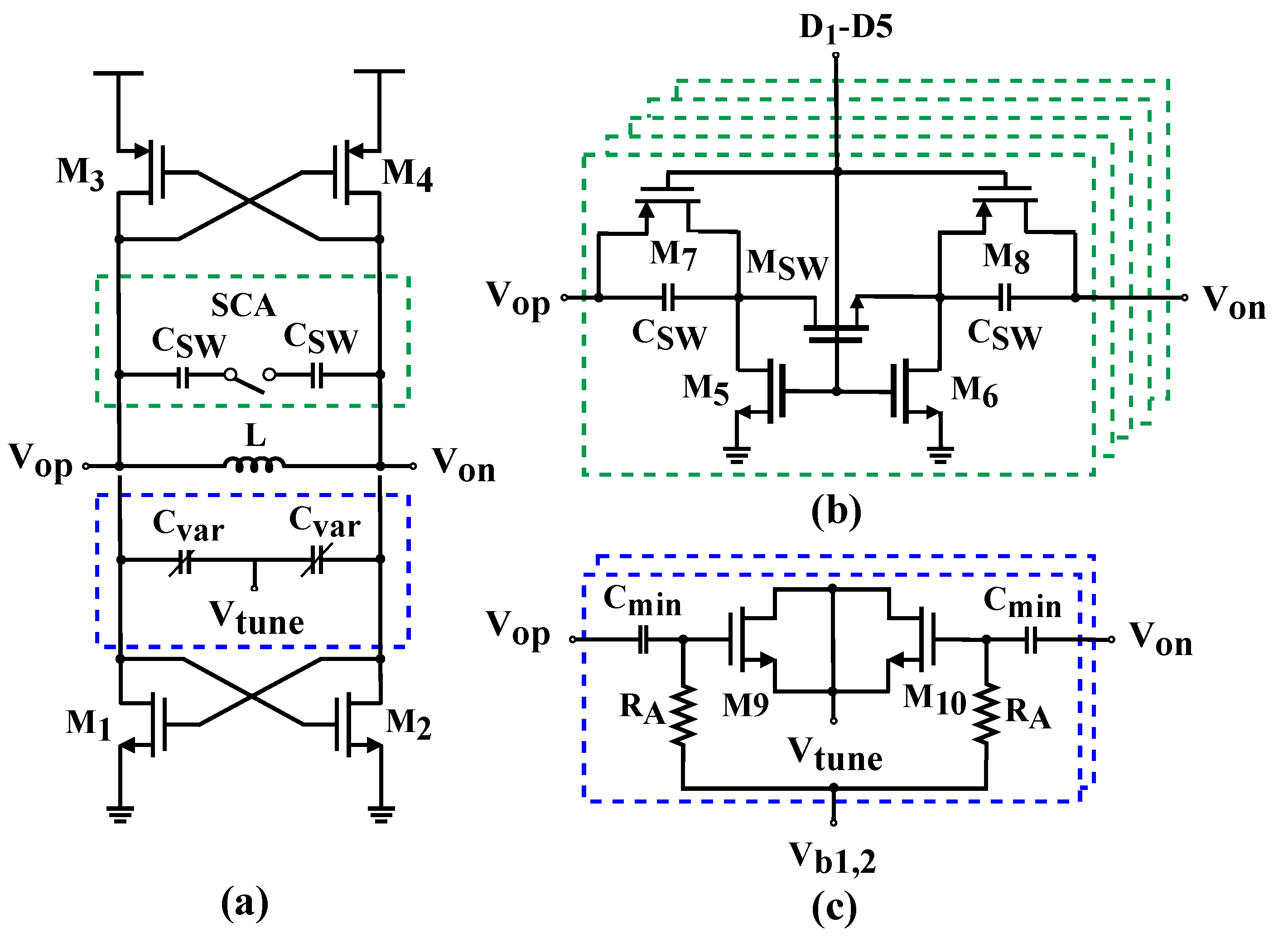
2.1. Phase-Locked Loop Design

The integer-N PLL using a wideband VCO is shown in Figure 3. The PLL crystal operates between 23 and 27 MHz, acting as the baseband and PLL clocks at the same time. A D-flip-flop-based PFD and programmable CP are designed to maintain stable loop dynamics. A second-order passive on-chip loop filter is selected to meet acceptable loop bandwidth and phase margin. A differential LC-VCO is used, followed by a high-speed current-mode logic (CML) divide by 2. The output of the LC-VCO and the divide by 2 are routed to the I/O pads through CML MUX. The PLL loop parameters and target PN at 100 kHz and 1 MHz offsets are tabulated in Table 1.

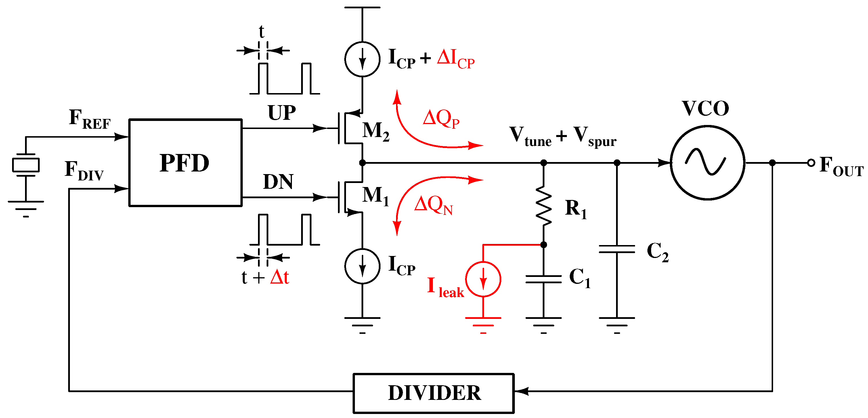
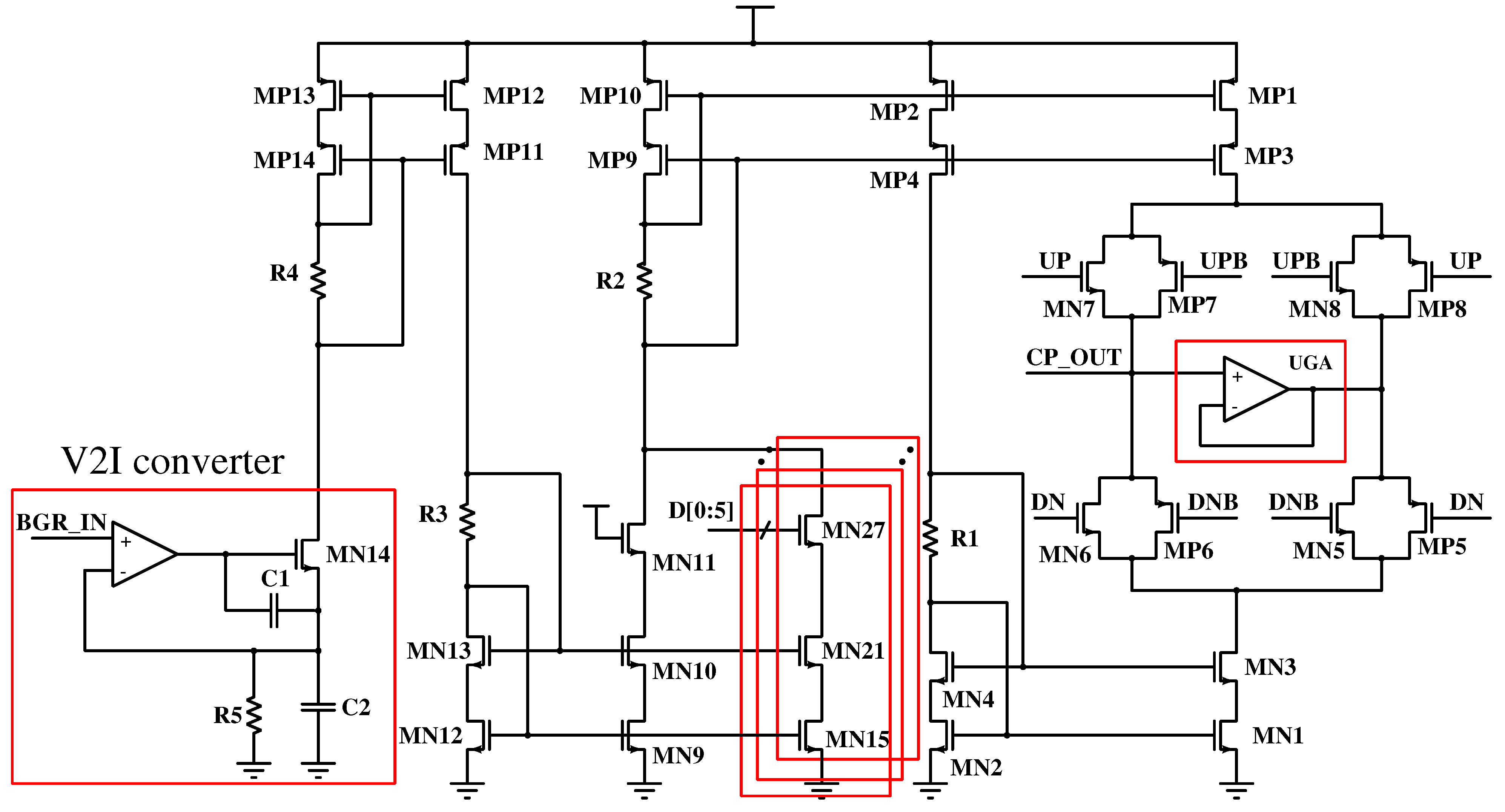
2.1.1. PFD and Charge Pump

A NAND gate-based PFD is implemented in this PLL [30]. It generates four outputs (UP, UPB, DN, and DNB) which are connected to the CP. A delay of ≈300 ps is added in the reset path to overcome the dead-zone issue. A programmable CP is designed to maintain an acceptable loop bandwidth and phase margin over the entire frequency range [30]. The I C P is programmable from 100 μ A to 1 mA (see Figure 9).

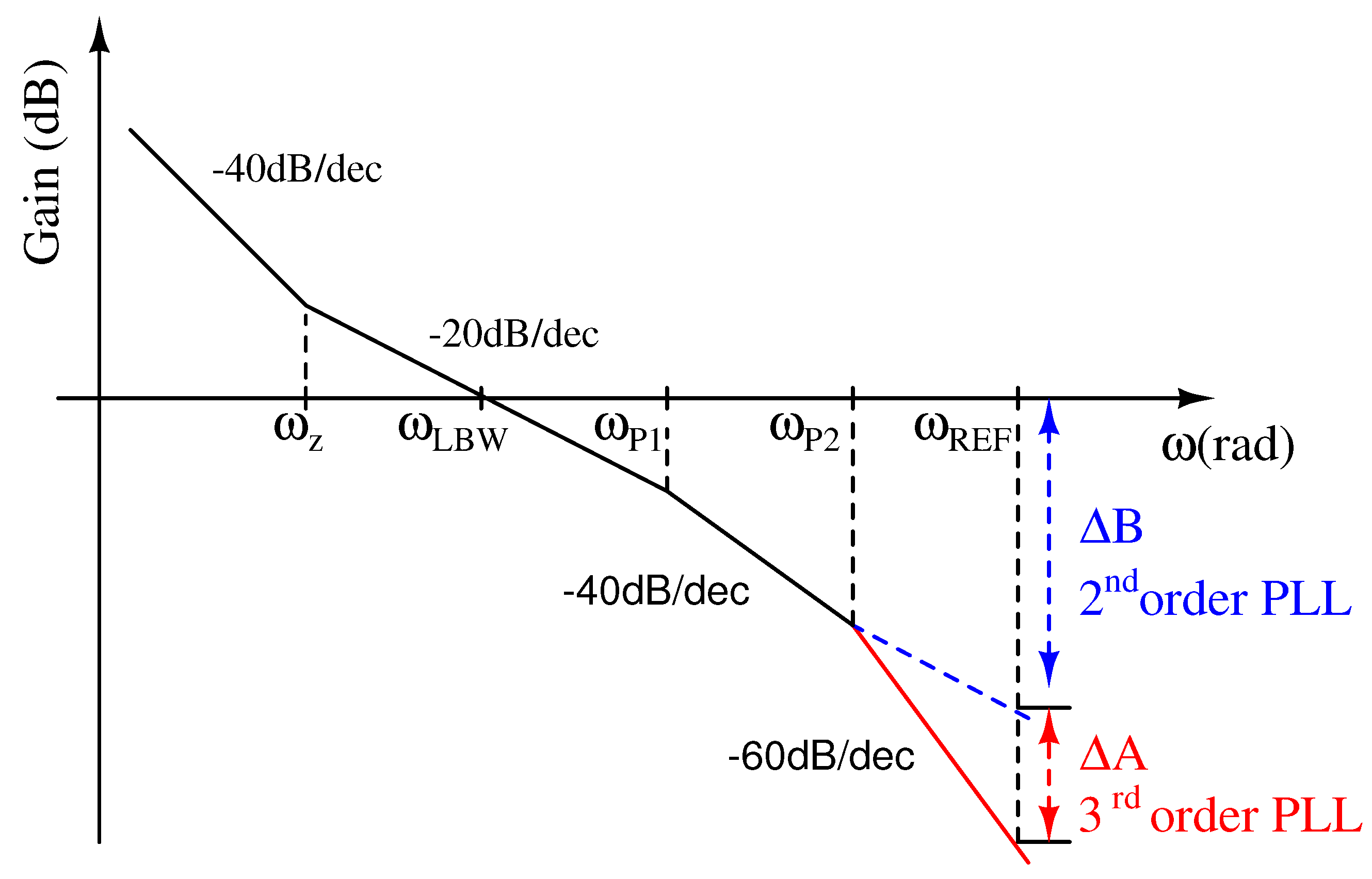
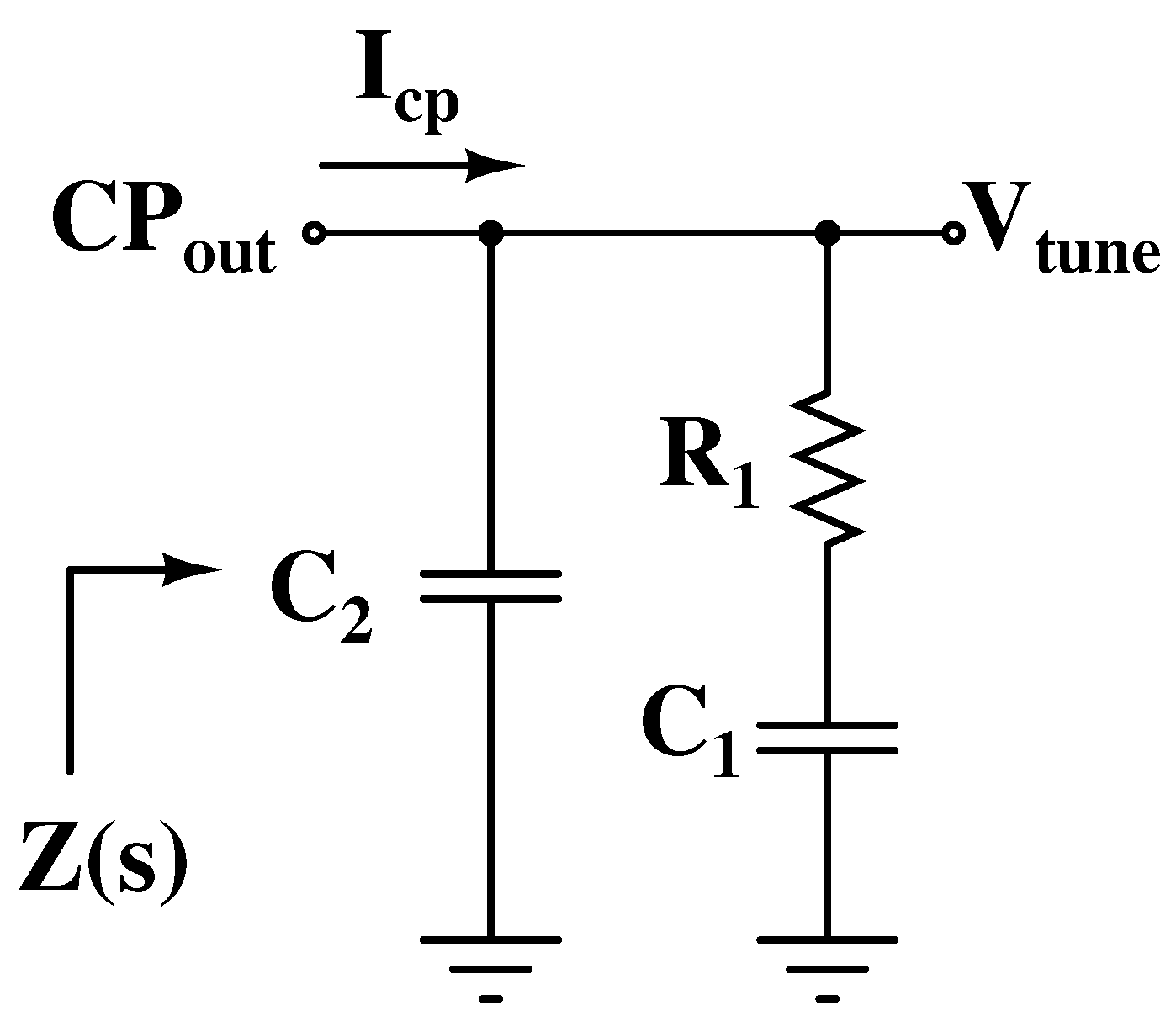
2.1.2. Second-Order Loop Filter

A Second-order passive loop filter for the charge-pump PLL is shown in Figure 10. There are two capacitors and one resistor. C 1 produces the first pole at the origin for this PLL. This is the largest capacitor, hence, it is a key integration bottleneck of the PLL and is used to generate a zero for loop stability. C 2 is used to smooth the control voltage ripples and to generate the second pole. The loop filter transimpedance, Z(s), is given by (12):
Z ( s ) = V t u n e ( s ) I c p ( s ) = 1 + s T z s ( C 1 + C 2 ) ( 1 + s T p )
where T z = R 1 · C 1 and T p = ( R 1 · C 1 · C 2 ) / ( C 1 + C 2 ) . After considering the stability criterion and settling time, the loop filter parameters are decided. The loop filter has a large capacitor ( C 1 ) to maintain better stability. This capacitor occupies the major area of the chip. The large spur attenuation requirement along with a large phase margin (≈60°) yields a large total integrated capacitance value that makes its integration challenging.

2.1.3. VCO and CML Divider

The VCO operates from 1.6 GHz to 3.2 GHz and generates the S-band from the VCO output in a differential way. The divide by 2 output generates the L 5 -band, which is quadratic in nature. Figure 11 shows the detailed schematic of the wideband LC-VCO. A complementary cross-coupled LC-VCO core is shown in Figure 11a. A dual-bias varactor shown in Figure 11b is used for fine tuning. The switched-capacitor array (SCA) structure implemented in [15] is used for discrete tuning as shown in Figure 11c.

2.1.4. Feedback Divider

Figure 12 shows an input ( f i n ) and output ( f o u t ) of a typical multi-modulus divider (MMD). The programming pin ( P i ), where i = 0 to N, and modulus control ( M I ) govern the division ratio. A suitable modulus out ( M O ) is generated based on the selection of M I and P i , acting as M I to the subsequent stage. A divide by three is produced when M I and P i are high. The 2 / 3 cell functions in a divide-by-two mode when M I is logic low, regardless of what P i is. An independent 2 / 3 MMD cell’s functioning is summed up in Table 2. The division ratio can be increased by inserting more of these 2 / 3 cells. In such cases, the M I of the final 2 / 3 stage is connected to the supply ( V D D ).
If the required division ratio of a PLL band falls outside the MMD range, this structure fails. The MMD division range is given by (13):
N = 2 0 P 0 + 2 1 P 1 + 2 2 P 2 + + 2 n P n
where n is the total number of 2 / 3 divider cells (n = 0, 1, 2, so on) and P i , where i = 0 to n, is the 2 / 3 cell digital control. Hence, the conventional MMD division range is limited from 2 n to 2 n + 1 1 . In this design, an MMD operating from 64 to 127 is incorporated in the feedback path.

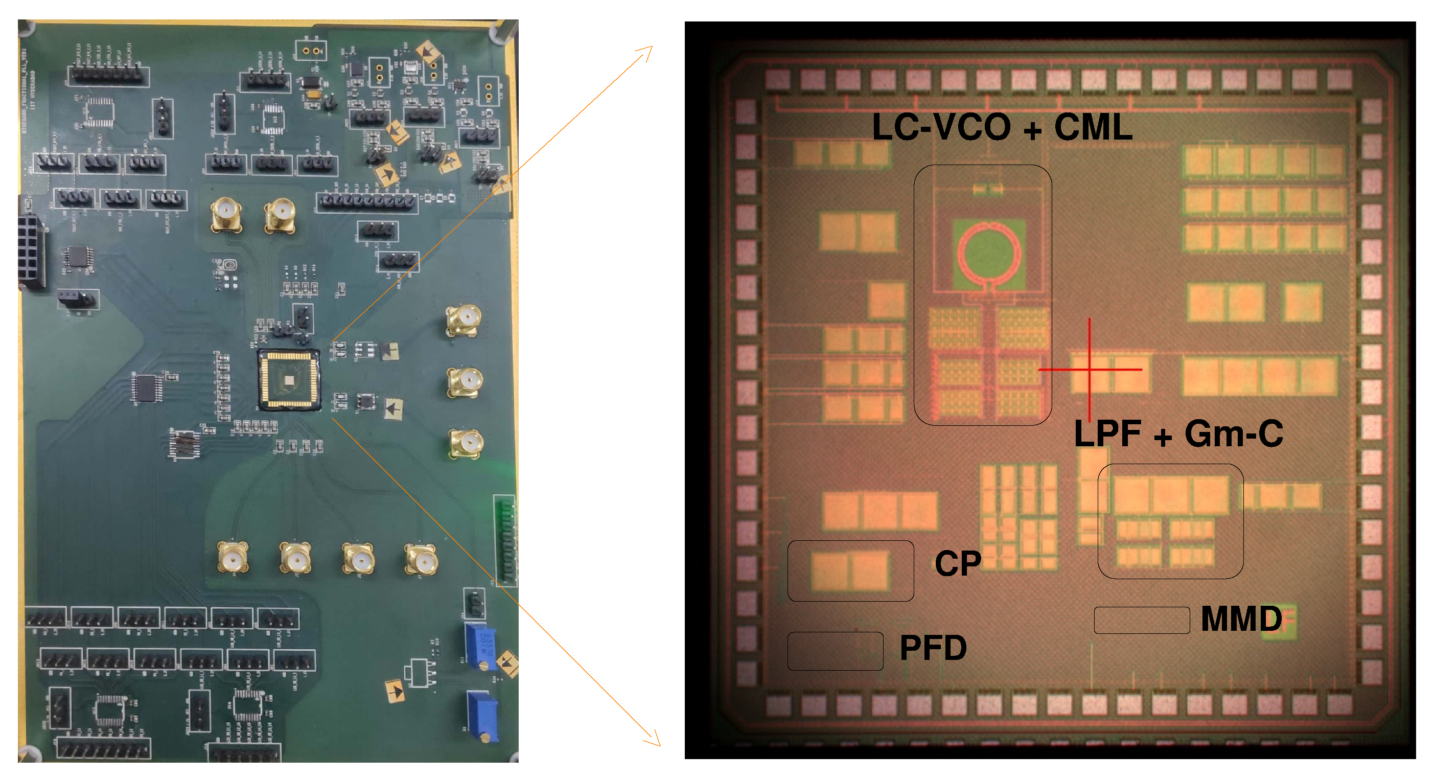
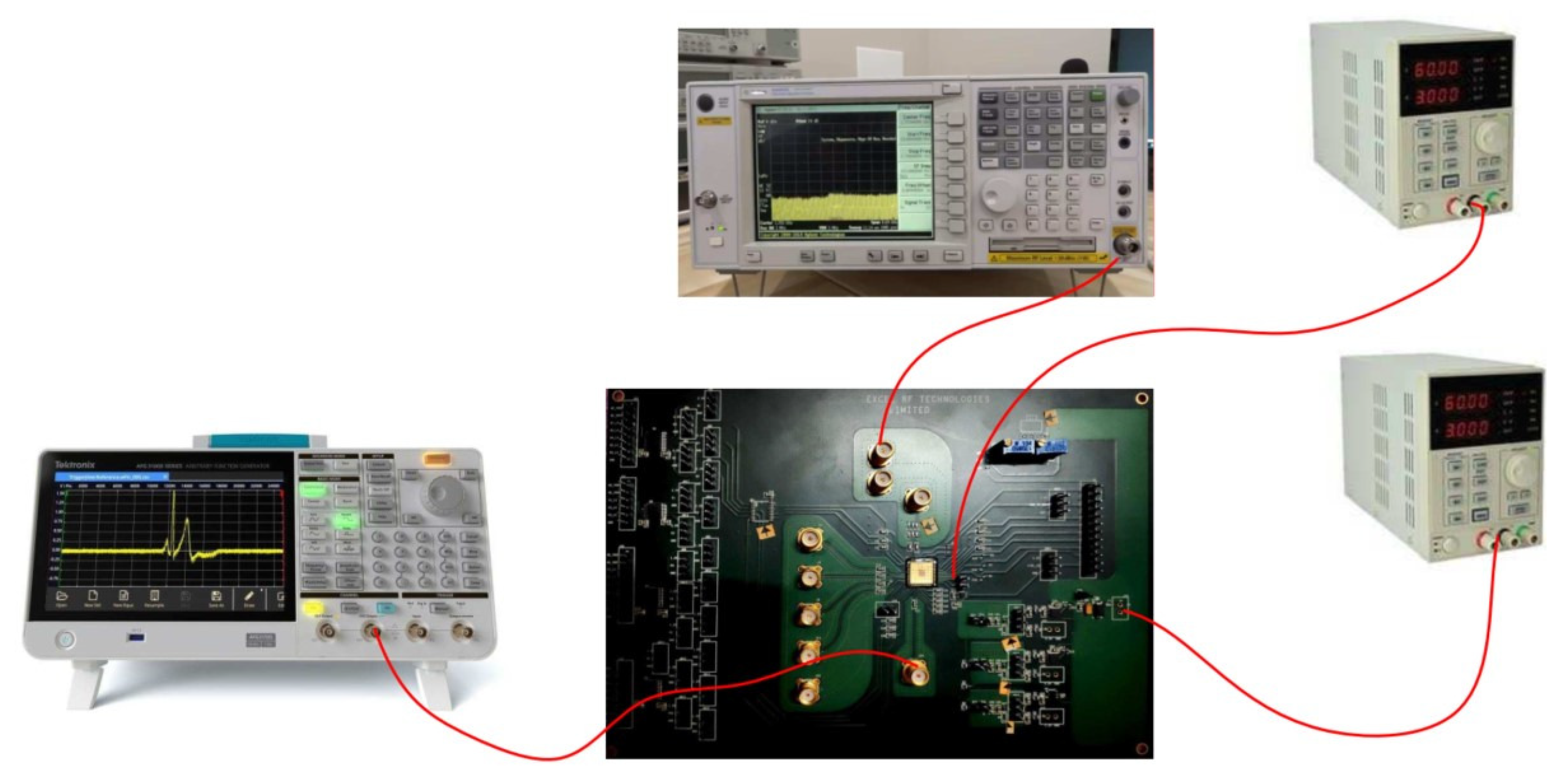
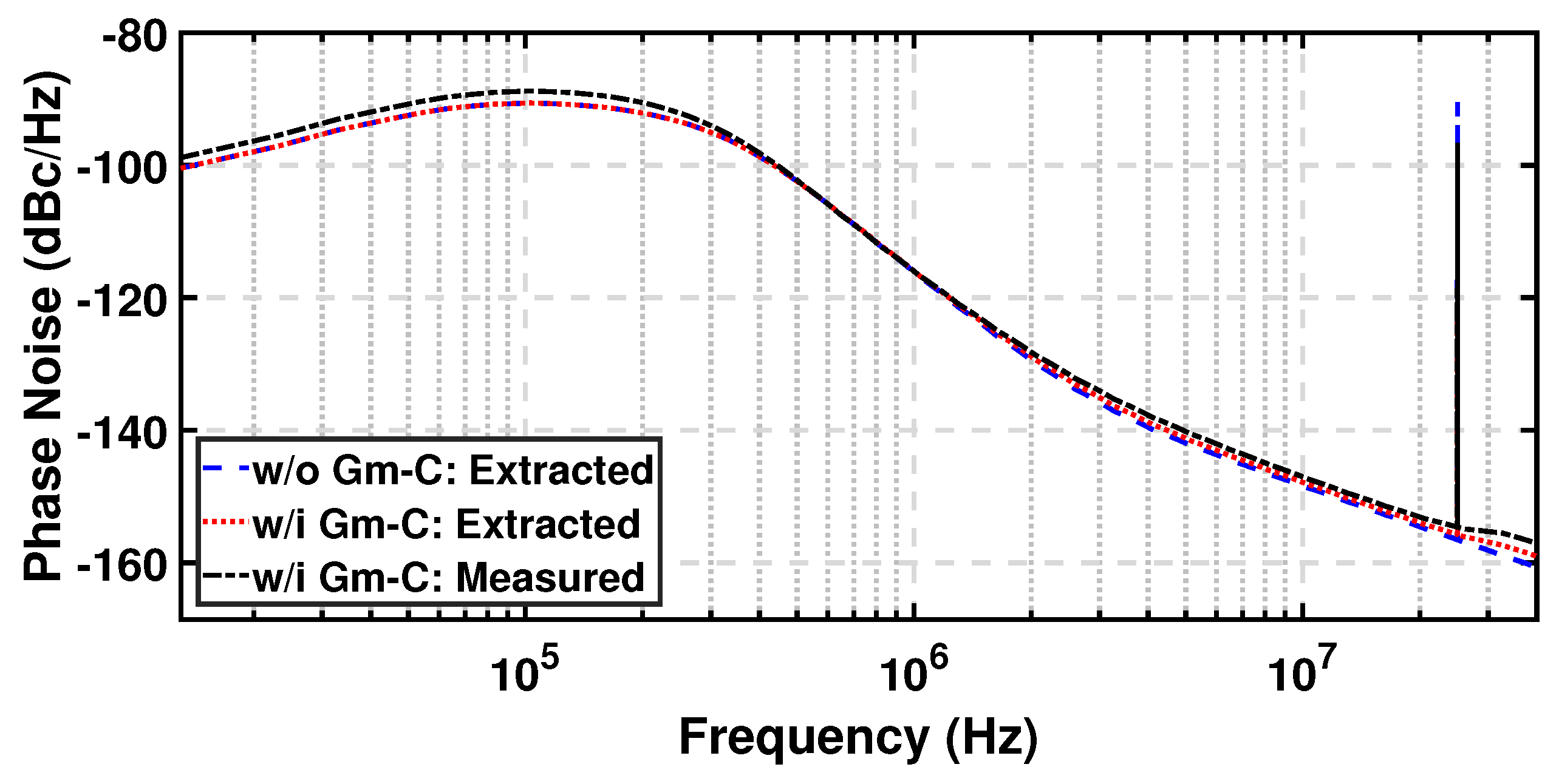
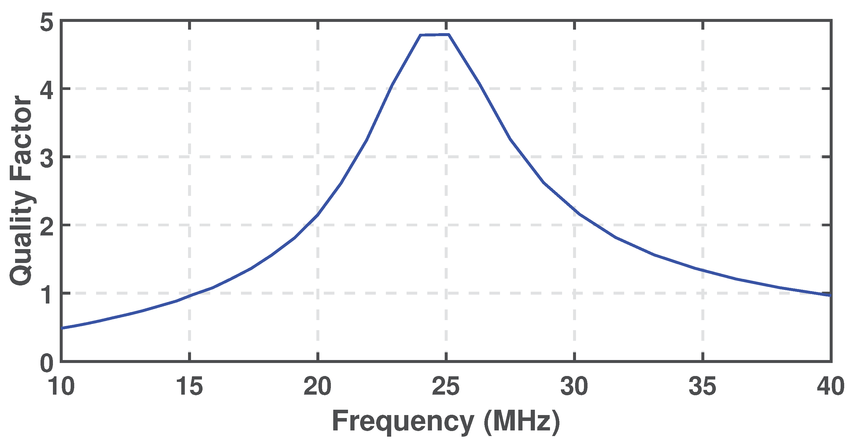
3. Measurement Results

The wideband PLL was fabricated in UMC 65 nm CMOS. The PLL operated from a supply voltage of 2.5 V for all blocks except the feedback divider which operated at 1.2 V. The VCO and the CML divider consumed 4 mA each, making the two most power-hungry blocks in the PLL. The complete PLL core area was 0.8 mm 2 .
The area of the VCO was 0.25 mm 2 (see Figure 13). A larger chip area was expected due to the on-chip inductor. The G m C notch filter had minimal area overhead ( 0.2 % of the loop filter). The test board with the die packaged in a 68-pin quad flat no-lead (QFN) package is shown in Figure 13. The measurement setup for the PLL is shown in Figure 14 [31].
The spectrum and phase noise were measured using an Agilent EXA N9010A signal analyzer. A function generator was used to provide the reference frequency to the PLL. The 25 MHz square-wave signal with a 50 % duty cycle was provided as the reference signal at the input of the PLL through the function generator. The proper control bits to generate 2.4 GHz output were chosen. The PLL output was connected to the spectrum analyzer using a radio frequency (RF) probe, and the phase noise was measured. The extracted simulation phase noise of the PLL with and without G m C and the measured phase noise of the PLL at a frequency of 2.4 GHz are shown in Figure 15.
The PLL spectrum at a 2.4 GHz LO frequency and reference spur at a 25 MHz offset is shown in Figure 16. A reference spur of ≈ 64 dBc was measured, which matched with the simulation results. Thus, the reference spur level was ≈7 dB better with the proposed G m C filter technique. The architecture comparison with other state-of-the-art active inductor based G m C filter implementations is shown in Table 3. The current consumption and circuit complexity of the proposed technique is lower compared to other works. Even though the supply of this work was 2.5 V, the proposed architecture is suitable for designs using a lower supply.
The performance comparison of the wideband PLL with state-of-the-art PLLs is summarized in Table 4. This work achieved the best figure of merit ( F o M ) of 171.3 dBc/Hz for the S-band compared to other works related to GPS applications. The F o M of the proposed wideband PLL was better than [18]. The reference spur in [26] was better but it came at the cost of an inferior PN, which is reflected in its F o M . The work in [32] was designed at a smaller power supply and lower technology node and achieved a better reference spur. The power consumption of this work is a bottleneck and can be reduced by lowering the supply and replacing the high-speed divide by two implemented using CML logic with TSPC logic.

4. Conclusions

An integer-N PLL for IRNSS applications was presented. The G m C filter design for reference spur reduction was analyzed. The simulation results showed that the proposed technique had no impact on the stability of the PLL. The Q factor of the G m C filter was also discussed. This design achieved a spur reduction with minimal area and power overhead. The design details of the PLL were discussed followed by measurement results to validate the design. The wideband PLL was incorporated with the proposed G m C filter-based spur reduction technique, which reduced the reference spur by ≈7 dB. This design thus offers a spur reduction technique with a simple approach rather than a complex amplifier approach. The only drawback of the proposed structure is the lack of programmability present in other works. In the future, programmability can be added in the G m C filter. A simple way is by replacing the C L with a varactor.

Author Contributions

Circuit idea, P.P.C.; circuit design/layout, P.P.C. and R.S.P.; on-wafer testing, P.P.C. and R.S.P.; writing—original draft preparation, P.P.C. and R.S.P.; writing—review and editing, P.P.C., R.S.P. and A.D. All authors have read and agreed to the published version of the manuscript.

Funding

This research is funded by MeitY, Government of India.

Data Availability Statement

Data are contained within the article.

Acknowledgments

The authors would like to thank MeitY, Government of India for the funding.

Conflicts of Interest

The authors declare no conflicts of interest.

References

  1. Ko, J.; Kim, J.; Cho, S.; Lee, K. A 19-mW 2.6-mm/sup 2/ L1/L2 dual-band CMOS GPS receiver. IEEE J. Solid-State Circuits 2005, 40, 1414–1425. [Google Scholar]
  2. Li, S.; Li, J.; Gu, X.; Wang, H.; Li, C.; Wu, J.; Tang, M. Reconfigurable All-Band RF CMOS Transceiver for GPS/GLONASS/Galileo/Beidou with Digitally Assisted Calibration. IEEE Trans. Very Large Scale Integr. Syst. 2015, 23, 1814–1827. [Google Scholar] [CrossRef]
  3. Hung, C.-M.; Kenneth, K.O. A fully integrated 1.5-V 5.5-GHz CMOS phase-locked loop. IEEE J. Solid-State Circuits 2002, 37, 521–525. [Google Scholar] [CrossRef]
  4. Li, A.; Chao, Y.; Chen, X.; Wu, L.; Luong, H.C. A Spur-and-Phase-Noise-Filtering Technique for Inductor-Less Fractional-N Injection-Locked PLLs. IEEE J. Solid-State Circuits 2017, 52, 2128–2140. [Google Scholar] [CrossRef]
  5. Lee, Y.; Seong, T.; Yoo, S.; Choi, J. A Low-Jitter and Low-Reference-Spur Ring-VCO-Based Switched-Loop Filter PLL Using a Fast Phase-Error Correction Technique. IEEE J. Solid-State Circuits 2018, 53, 1192–1202. [Google Scholar] [CrossRef]
  6. Seong, T.; Lee, Y.; Yoo, S.; Choi, J. A 320-fs RMS Jitter and −75-dBc Reference-Spur Ring-DCO-Based Digital PLL Using an Optimal-Threshold TDC. IEEE J. Solid-State Circuits 2019, 54, 2501–2512. [Google Scholar] [CrossRef]
  7. Yang, Z.; Chen, Y.; Mak, P.-I.; Martins, R.P. A Calibration-Free, Reference-Buffer-Free, Type-I Narrow-Pulse-Sampling PLL with −78.7-dBc REF Spur, −128.1-dBc/Hz Absolute In-Band PN and −254-dB FOM. IEEE-Solid-State Circuits Lett. 2020, 3, 494–497. [Google Scholar] [CrossRef]
  8. Yang, Z.; Chen, Y.; Mak, P.-I.; Martins, R.P. A 0.003-mm2 440fsRMS-Jitter and −64dBc-Reference-Spur Ring-VCO-Based Type-I PLL Using a Current-Reuse Sampling Phase Detector in 28-nm CMOS. IEEE Trans. Circuits Syst. I Regul. Pap. 2021, 68, 2307–2316. [Google Scholar] [CrossRef]
  9. Seol, J.-H.; Choo, K.; Blaauw, D.; Sylvester, D.; Jang, T. Reference Oversampling PLL Achieving −256-dB FoM and −78-dBc Reference Spur. IEEE J. Solid-State Circuits 2021, 56, 2993–3007. [Google Scholar] [CrossRef]
  10. Huang, Y.; Chen, Y.; Jiao, H.; Mak, P.-I.; Martins, R.P. A 3.36-GHz Locking-Tuned Type-I Sampling PLL with −78.6-dBc Reference Spur Merging Single-Path Reference-Feedthrough-Suppression and Narrow-Pulse-Shielding Techniques. IEEE Trans. Circuits Syst. II Express Briefs 2021, 68, 3093–3097. [Google Scholar] [CrossRef]
  11. Liang, Y.; Boon, C.C. A 40 GHz CMOS PLL with −75-dBc Reference Spur and 121.9-fsrms Jitter Featuring a Quadrature Sampling Phase-Frequency Detector. IEEE Trans. Microw. Theory Tech. 2022, 70, 2299–2314. [Google Scholar] [CrossRef]
  12. Liang, Y.; Boon, C.C.; Chen, Q. A 23.4 mW −72-dBc Reference Spur 40 GHz CMOS PLL Featuring a Spur-Compensation Phase Detector. IEEE Microw. Wirel. Components Lett. 2022, 32, 1091–1094. [Google Scholar] [CrossRef]
  13. Huang, Y.; Chen, Y.; Zhao, B.; Mak, P.-I.; Martins, R.P. A 3.6-GHz Type-II Sampling PLL with a Differential Parallel-Series Double-Edge S-PD Scoring 43.1-fsRMSJitter, −258.7-dB FOM, and −75.17-dBc Reference Spur. IEEE Trans. Very Large Scale Integr. (VLSI) Syst. 2023, 31, 188–198. [Google Scholar] [CrossRef]
  14. Verma, A.; Bhagavatula, V.; Singh, A.; Wu, W.; Nagarajan, H.; Lau, P.; Yu, X.; Elsayed, O.; Jain, A.; Sarkar, A.; et al. A 16-Channel, 28/39GHz Dual-Polarized 5G FR2 Phased-Array Transceiver IC with a Quad-Stream IF Transceiver Supporting Non-Contiguous Carrier Aggregation up to 1.6GHz BW. In Proceedings of the IEEE International Solid-State Circuits Conference (ISSCC), San Francisco, CA, USA, 18–22 February 2024; pp. 1–3. [Google Scholar]
  15. Chary, P.P.; Peerla, R.S.; Pula, B.T.; Dutta, A.; Sahoo, B.D. Package Aware LC-VCO with Self-Biased Switched Capacitor Structure for Better Supply Noise Rejection. IEEE TRans. Components Packag. Manuf. Tech. 2022, 12, 1653–1660. [Google Scholar] [CrossRef]
  16. Shi, C.; Wang, C.; Ye, L.; Liao, H. 99 dBc/Hz @ 10 KHz 1 MHz-step dual-loop integer-N PLL with anti-mislocking frequency calibration for global navigation satellite system receiver. In Proceedings of the 2011 IEEE International Symposium of Circuits and Systems (ISCAS), Rio de Janeiro, Brazil, 15–18 May 2011; pp. 1876–1879. [Google Scholar]
  17. Bai, Z.; Zhou, X.; Mason, R.D.; Allan, G. A 2-GHz Pulse Injection-Locked Rotary Traveling-Wave Oscillator. IEEE Trans. Microw. Theory Tech. 2016, 64, 1854–1866. [Google Scholar] [CrossRef]
  18. Kharalkar, A.; Pancholi, M.; Kanchetla, V.K.; Khade, A.; Khyalia, S.; Hameed, S.; Zele, R. A Compact, Low-Phase Noise Fractional-N PLL for Global Navigation Receiver. In Proceedings of the IEEE 19th New Circuits and Systems Conference (NEWCAS), Toulon, France, 13–16 June 2021; pp. 1–4. [Google Scholar]
  19. Peerla, R.S.; Chary, P.; Dutta, A.; Sahoo, B.D. A Dual VCO Based L5/S Band PLL with Extended Range Divider for IRNSS Application. In Proceedings of the IEEE International Symposium on Circuits and Systems (ISCAS), Austin, TX, USA, 27 May–1 June 2022; pp. 1699–1703. [Google Scholar]
  20. Shaik Peerla, R.; Dutta, A.; Sahoo, B.D. An Extended Range Divider Technique for Multi-Band PLL. J. Low Power Electron. Appl. 2023, 13, 43. [Google Scholar] [CrossRef]
  21. Elsayed, M.M.; Abdul-Latif, M.; Sanchez-Sinencio, E. A Spur-Frequency-Boosting PLL with a −74 dBc Reference-Spur Suppression in 90 nm Digital CMOS. IEEE J. Solid-State Circuits 2013, 48, 2104–2117. [Google Scholar] [CrossRef]
  22. Rhee, W. Design of high-performance CMOS charge pumps in phase-locked loops. In Proceedings of the IEEE International Symposium on Circuits and Systems (ISCAS), Orlando, FL, USA, 30 May–2 June 1999; Volume 2, pp. 545–548. [Google Scholar]
  23. Lin, T.H.; Kaiser, W.J. A 900-MHz 2.5-mA CMOS frequency synthesizer with an automatic SC tuning loop. IEEE J. Solid-State Circuits 2001, 36, 424–431. [Google Scholar]
  24. Gao, X.; Klumperink, E.A.; Socci, G.; Bohsali, M.; Nauta, B. Spur Reduction Techniques for Phase-Locked Loops Exploiting A Sub-Sampling Phase Detector. IEEE J. Solid-State Circuits 2010, 45, 1809–1821. [Google Scholar] [CrossRef]
  25. Lee, T.; Lee, W. A Spur Suppression Technique for Phase-Locked Frequency Synthesizers. In Proceedings of the IEEE International Solid-State Circuits Conference (ISSCC), San Francisco, CA, USA, 6–9 February 2006; pp. 2432–2441. [Google Scholar]
  26. Ko, H.G.; Bae, W.; Jeong, G.S.; Jeong, D.K. Reference Spur Reduction Techniques for a Phase-Locked Loop. IEEE Access 2019, 7, 38035–38043. [Google Scholar] [CrossRef]
  27. Sharma, J.; Krishnaswamy, H. A 2.4-GHz Reference-Sampling Phase-Locked Loop That Simultaneously Achieves Low-Noise and Low-Spur Performance. IEEE J. Solid-State Circuits 2019, 54, 1407–1424. [Google Scholar] [CrossRef]
  28. Kong, L.; Razavi, B. A 2.4 GHz 4 mW Integer-N Inductorless RF Synthesizer. IEEE J. Solid-State Circuits 2016, 51, 626–635. [Google Scholar] [CrossRef]
  29. Cheng, X.; Chen, F.J.; Zhang, L.; Gao, H.; Han, J.A.; Han, J.Y.; Yu, Y.; Deng, X.J. A Closed-Loop Reconfigurable Analog Baseband Circuitry with Open-Loop Tunable Notch Filters to Improve Receiver Tx Leakage and Close-in Blocker Tolerance. IEEE Trans. Circuits Syst. II Express Briefs 2022, 69, 839–843. [Google Scholar] [CrossRef]
  30. Razavi, B. Design of CMOS Phase-Locked Loops: From Circuit Level to Architecture Level; Cambridge University Press: Cambridge, UK, 2020. [Google Scholar]
  31. Lavrič, A.; Batagelj, B.; Vidmar, M. Calibration of an RF/Microwave Phase Noise Meter with a Photonic Delay Line. Photonics 2022, 9, 533. [Google Scholar] [CrossRef]
  32. Wu, W.; Yao, C.W.; Guo, C.; Chiang, P.Y.; Chen, L.; Lau, P.K.; Bai, Z.; Son, S.W.; Cho, T.B. A 14-nm Ultra-Low Jitter Fractional-N PLL Using a DTC Range Reduction Technique and a Reconfigurable Dual-Core VCO. IEEE J. Solid-State Circuits 2021, 56, 3756–3767. [Google Scholar] [CrossRef]
Figure 1. Block diagram of integer-N PLL depicting the causes of reference spur due to various mismatches.
Jlpea 14 00017 g001
Figure 2. Graphical representation showing how the order of the loop filter impacts the reference spur of the PLL.
Jlpea 14 00017 g002
Figure 3. Block diagram of PLL with reference spur reduction using a notch filter.
Jlpea 14 00017 g003
Figure 4. Active inductor implementation used in [28] for G m C filter.
Jlpea 14 00017 g004
Figure 5. LC−filter block level realization using G m C structure (a) and circuit level implementation (b).
Jlpea 14 00017 g005
Figure 6. Quality factor plot for the G m C filter with a best Q-factor at ≈5 for a frequency of 25 MHz.
Jlpea 14 00017 g006
Figure 7. Phase and magnitude plots showing the PLL stability with and without the G m C filter.
Jlpea 14 00017 g007
Figure 8. PLL spectrum depicting the reference spur at 25 MHz with and without G m C .
Jlpea 14 00017 g008
Figure 9. Single-ended programmable charge pump using a switch at the drain topology.
Jlpea 14 00017 g009
Figure 10. Second order passive low pass filter.
Jlpea 14 00017 g010
Figure 11. (a) Cross-coupled LC-VCO core, (b) self-biased switched capacitor array, and (c) dual-biased varactor for linearization [15].
Jlpea 14 00017 g011
Figure 12. Block diagram of conventional 2 / 3 cell-based MMD structure.
Jlpea 14 00017 g012
Figure 13. PCB mounted by the wideband PLL die along with the die micrograph highlighting the sub-blocks of the PLL.
Jlpea 14 00017 g013
Figure 14. Measurement setup depicting the power supply and spectrum analyzer used for the characterization of the PLL.
Jlpea 14 00017 g014
Figure 15. Simulated and measured PLL PN with and without G m C .
Jlpea 14 00017 g015
Figure 16. PLL spectrum with reference spur when LO is at 2.4 GHz.
Jlpea 14 00017 g016
Table 1. PLL Loop parameters.
ParameterValue
Crystal frequency (MHz)23 to 27
VCO range (GHz)1.6 to 3.2
VCO gain (MHz/V)80 to 120
I C P (mA)0.1 to 1
Division ratio64 to 127
Loop bandwidth (kHz)160 to 240
Phase margin (°)54 to 59
PN @ 100 kHz (dBc/Hz)−90 to −95
PN @ 1 MHz (dBc/Hz)−115 to −120
Table 2. Working of standalone 2 / 3 MMD cell.
Input ( IN ) P i MI Output ( OUT )
f i n X0 f i n / 2
f i n 01 f i n / 2
f i n 11 f i n / 3
Table 3. Architecture comparison between various G m C filter implementation techniques.
This Work[28][29]
Supply (V)2.51.31.8
G m C Architecture (V)Single endedDifferentialDifferential
Operational amplifier in
L e q implementation
NoYes
(Single ended)
Yes
(Fully differential)
Circuit ComplexityLowModerateHigh
Current (mA)0.20.41.5
Compatible with
lower supply
YesNoNo
ProgrammabilityNo †YesYes
† Programmability can be added but was not added in this work.
Table 4. Performance comparison of wideband PLLs.
This Work[18][26][32]
Technology (nm)65656514
Supply (V)2.5/1.21.21.31/0.8
Frequency (GHz)1.6–3.21.17–2.50.85–7
Reference (MHz)23–2723–275076.8
PN (dBc/Hz)
@ 1 MHz
−116/−122−116−110−122
Area ( mm 2 )0.80.250.9350.31
Power (mW)3015.74.814.2
Ref. spur (dBc)−64 (−57 ‡)NA−68.57−69.6
FoM †171.3165.4161.25186.6
† FoM = 10 × log f v c o / Δ f 2 . 1 m W / P o w . P N . ‡ Extracted simulation without G m C .
Disclaimer/Publisher’s Note: The statements, opinions and data contained in all publications are solely those of the individual author(s) and contributor(s) and not of MDPI and/or the editor(s). MDPI and/or the editor(s) disclaim responsibility for any injury to people or property resulting from any ideas, methods, instructions or products referred to in the content.

