Article

An Ultra-Low-Voltage Approach to Accurately Set the Quiescent Current of Digital Standard Cells Used for Analog Design and Its Application on an Inverter-Based Operational Transconductance Amplifier

by
Riccardo Della Sala
*,
Francesco Centurelli
and
Giuseppe Scotti
Department of Information Electronic and Telecommunication (DIET), Sapienza University of Rome, Via Eudossiana 18, 00184 Rome, Italy
*
Author to whom correspondence should be addressed.
J. Low Power Electron. Appl. 2024, 14(3), 39; https://doi.org/10.3390/jlpea14030039
Submission received: 7 June 2024 / Revised: 16 July 2024 / Accepted: 22 July 2024 / Published: 24 July 2024
(This article belongs to the Special Issue Ultra-Low-Power ICs for the Internet of Things Vol. 2)

Abstract

:
An approach to design analog building blocks based on digital standard cells is presented in this work. By ensuring that every CMOS inverter from a standard-cell library operates with a well-defined quiescent current and output voltage, the suggested method makes it possible to construct analog circuits that are resistant against PVT variations. The method uses the local supply voltages connected to the source terminals of the p-channel and n-channel MOS transistors of the standard-cell inverters as control inputs. It is based on adaptive supply voltage generator (ASVG) reusable blocks, which are comparable to those used in digital applications to handle process variations. All of the standard-cell inverters used for analog functions receive the local supply voltages produced by the ASVGs, which enable setting each cell’s quiescent current to a multiple of a reference current and each cell’s static output voltage to an appropriate reference voltage. Both the complete custom design of the ASVG blocks and a theoretical study of the feedback loop of the ASVG are presented. An application example through the design of a fully synthesizable two-stage operational transconductance amplifier (OTA) is also provided. The TSMC 180 nm CMOS technology has been used to implement both the OTA and the ASV generators. Simulation results have demonstrated that the proposed approach allows to accurately set the quiescent current of standard-cell inverters, dramatically reducing the effect of PVT variations on the pmain performance parameters of the standard-cell-based two-stage OTA.

1. Introduction

The evolution of technology has made electronics more and more pervasive [1,2,3]. Modern electronic systems are essentially digital systems [4] with analog interfaces, enabling them to interact with the real world [5,6,7]. However, even if the analog part often constitutes just a small fraction of the overall system, its design typically requires the most effort since it is a custom, trial-and-error process, compared to the fully automated design and layout of the digital part [8,9,10,11,12,13,14,15]. For this reason, research is ongoing to automate the design of analog blocks, or at least use automatic place and route tools for the layout phase, to speed up the marketing time and improve the portability of designs across different technologies [16]. In this context, an interesting research field concerns the use of digital standard cells to design analog blocks that are compatible with the automatic place and route tools of the digital design flow [17,18,19,20,21].
Two approaches are possible to design standard-cell-based analog blocks: the analog functions can be rethought from basic principles to implement them in the digital domain (e.g., DIGOTA [13,14,20,22], dyadic pulse DAC [23,24,25,26]). On the other hand, standard cells can be exploited to mimic the basic analog building blocks and reproduce analog circuit topologies [9,18,19,27,28]. The latter approach allows a better control of the circuits’ analog performance and is more familiar to the analog designer; however, it requires the designer to cope with the variations of process parameters, temperature, and supply voltage (PVT).
A typical field of application for such circuits is that of ultra-low-voltage (ULV) and ultra-low-power (ULP) systems [29] for biomedical and Internet of Things (IoT) systems [30,31,32,33,34,35,36] that include a large digital part, with a low supply voltage (0.3–0.5 V) limiting the use of standard analog approaches such as differential pairs and cascode [37,38,39,40]. To implement analog functions such as amplifiers and filters [41,42,43,44], body driving and inverter-based stages are the most common options [37,45,46,47,48,49,50,51,52,53,54,55,56]. For blocks at the edge of the analog and digital worlds, such as comparators, the use of standard cells allows an efficient implementation of low-voltage latches [57,58,59,60,61].
In absence of the tail current generator, which is not compatible with the ULV environment, controlling the bias point of gain stages and hence the performance of the amplifiers (gain, gain–bandwidth product)—with respect to variations in PVT and input common-mode voltage—is extremely difficult [19,27]. Body biasing is a solution that is often adopted in inverter-based stages [45,62], but it is compatible only with standard-cell families where body voltage rails are explicitly accessible.
An approach to center the input–output transfer characteristic of standard-cell inverters to keep the DC output voltage constant has been recently proposed in [27]. This allows us to design robust amplifiers, such as a cascade of inverter stages, keeping them optimally biased [18,28]; however, this also provides no control of the inverters’ quiescent current and hence on their transconductance (and consequently on the gain–bandwidth product of amplifiers based on such inverters). The quiescent current is in fact affected by PVT variations of the threshold voltage of devices [51], and this causes huge variations of the transconductance, especially in standard-cell inverters biased in the sub-threshold region [9,45].
Adaptive supply voltage scaling (ASV) is often utilized by digital designers to cope with PVT variations and to reduce the spread of the maximum operating frequency and power consumption of digital circuits [63,64,65]. In these approaches, specific adaptive supply voltage generators (ASVGs) are exploited to provide local supply voltage for optimizing the speed/power consumption trade-off [66]. These blocks are typically designed following a full-custom approach, similarly to the standard cells in the digital libraries of a given technology. Once all the needed files are available, ASVGs can be used in a semi-custom design flow, where the layout step is performed by an automatic place and route tool.
In this work, we propose a novel approach in which suitable ASVGs are exploited to keep the bias current of digital standard cells used for analog design constant by generating suitable values of local supply voltages V D D c t r l and V S S c t r l in order to counteract the effects of PVT variations on the quiescent current. The proposed approach is applied to the design of a simple two-stage inverter-based OTA implemented with standard-cell inverters. Simulation results referring to the standard-cell library of a 180 nm CMOS technology highlight the capability of the proposed methodology to dramatically reduce the spread of main OTA performance parameters with respect to the conventional design. In Section 2, we present both a theoretical study and simulation results of the conventional standard-cell-based two-stage OTA operating in sub-threshold to highlight the strong impact of PVT variations on the main OTA parameters. The proposed approach to set the quiescent current of standard-cell inverters and its application to a standard-cell-based two-stage OTA are discussed in Section 3, the results of parametric and Monte Carlo simulations are presented in Section 4, and some conclusion are drawn in Section 5.

2. Two-Stage Standard-Cell-Based OTA Operating in Sub-Threshold

To explain the proposed approach in detail, we refer, as a case study, to the conventional two-stage inverter-based OTA implemented with standard-cell inverters. The topology of the two-stage inverter-based OTA is depicted in Figure 1. The first stage is composed using I 1 4 , which implement a standard-cell-based differential to a single-ended converter [19], whereas the second stage is composed using I 5 , implementing the inverting output stage. Although it is simple, this architecture is very effective for highlighting the main limitations that come from the adoption of a standard-cell approach to analog design, in which analog blocks are directly connected to the supply voltages V D D and V S S , without any control of the bias current of standard-cell inverters.

2.1. Characterization of the CMOS Inverter Operating in Sub-Threshold and Transfer Matrix

For the following analysis, we denote the input capacitance of the generic i-th inverter with C g s i , which is given by the sum of the gate-source capacitances C g s n , p i of the NMOS and PMOS transistors of the inverter, with C g d i being the sum of the gate-drain capacitances C g d n , p i , g m i being the sum of the transconductances g m n , p i of the NMOS and PMOS transistors of the inverter, and with g d s i being the sum of output conductances g d s n , p i of the NMOS and PMOS transistors of the inverter. By using this notation, the inverter’s transfer matrix input voltage, output voltage, and currents can be written as follows:
V I n I I n = A B C D × V O u t I O u t
where
A = g d s i g m i 1 + s C g d i / g d s i
B = s · C g s i + g m i / g d s i · C g d i · g d s i g m i · 1 + s C g d i / g d s i
C = 1 / g m i
and, finally,
D = s · C g s i + g m i / g d s i · C g d i g m i
As it can be observed, the coefficients of the inverter’s transfer matrix depend on terms g m i and g d s i . These terms rely on the quiescent current of the NMOS and PMOS transistors of the inverter which, due to the operation in the sub-threshold region, can be expressed as follows:
I d n = I d 0 n e V g s n V t h n n U t 1 e V d s n U t NMOS I d p = I d 0 p e V s g p + V t h p n U t 1 e V s d p U t PMOS
where usual notation is adopted for gate-source, drain-source, and threshold voltages of NMOS and PMOS transistors; U t denotes the thermal voltage; and n = 1 + C d e p l / C o x and I d 0 can be written as follows:
I d 0 n , p = μ n , p ( n 1 ) C o x W n , p L n , p U t 2
where μ n , p and C o x are the mobility and oxide capacitance per unit area, whereas W n , p and L n , p are the gate width and gate length of NMOS and PMOS devices, respectively.
It is evident from the above equations that the quiescent current of MOS devices, and therefore the small signal parameters of the inverter, are strongly dependent on PVT variations. This has a strong impact on the performance parameters of the conventional two-stage standard-cell-based OTA, as it will be better pointed out in the next subsections.

2.2. Analytical Characterization of the Standard-Cell-Based Two-Stage OTA

The most important performance parameters of an OTA are the gain–bandwidth product (GBW), the phase margin ( m φ ), the differential voltage gain ( A v D ), the power consumption ( P d ), and the average slew rate ( S R a v g ). Referring to the OTA in Figure 1, using the notation introduced in Section 2.1, and denoting the load capacitance of the OTA with C L , the main performance parameters of the OTA can be easily expressed as follows:
A v D = 1 2 1 + g m 2 g m 3 · g m 1 g d s 4 + g d s 1 · g m 5 g d s 5 · 1 1 + s C L / g d s 5
G B W = 1 2 1 + g m 2 g m 3 · g m 1 g d s 4 + g d s 1 · g m 5 C L
m φ = 180 a r c t a n G B W · g d s 4 + g d s 1 C g s 5 a r c t a n G B W · g d s 5 C L
S R a v g = I d 0 e V D D V t h n n U t + I d 0 e V D D V t h p n U t 2
As it can be observed, all the terms in the above equations depend on g m i and g d s i of the inverters, which, as discussed in Section 2.1, are strongly dependent on the supply voltages, which set the value of gate-source and drain-source voltages, the temperature (due to the temperature dependence of parameters such as U t or I d 0 n , p ), and process variations (due to the dependence of V t h on process steps).
All these considerations allow us to conclude that the conventional standard-cell-based two-stage OTA exhibits performance parameters that strongly dependent on PVT variations. This point will be further assessed in the next section through transistor-level simulations.

2.3. Simulation Results on the Conventional Standard-Cell-Based Two-Stage OTA Operating in Sub-Threshold without Quiescent Current Control

The two-stage standard-cell-based OTA reported in Figure 1 was designed in reference to the standard-cell library of the TSMC 180 nm CMOS technology with a nominal supply voltage V D D V S S of 0.35 V. Transistor-level simulations were carried out within the Cadence Virtuoso environment. To quantify the dependence of performance parameters on PVT variations, parametric and corner simulations were executed. The results are summarized in Table 1, where V o f f denotes the error with respect to the ideal DC output voltage of the OTA in a unity–gain feedback configuration and where Itot is the total current drawn by the OTA. The first five columns in the table (from Typ to FS) refer to the five process corners of the technology, the sixth and seventh column refer to supply voltage variations, and the last two columns refer to temperature variations.
The results of process-only and mismatch-only Monte Carlo simulations are reported in Table 2 and Table 3, respectively. The histograms of GBW, Pd, and m φ under process-only and mismatch-only Monte Carlo simulations are reported in Figure 2 and Figure 3, respectively.
As it can be observed in all the above tables and figures, the quiescent current of the standard-cell inverters operating in a sub-threshold exhibits huge variations, resulting in large variations in the GBW and m φ of the OTA. Due to this behavior, the applicability of this OTA to signal processing systems presents many difficulties and drawbacks, and its usage is not justified. In order to make this standard-cell-based OTA usable in real applications, the quiescent current of the inverters should be controlled to at least reduce variations with respect to temperature and process variations.

3. Proposed Approach to Set the Quiescent Current of Standard-Cell Inverters and Application to a Standard-Cell-Based OTA

In the conventional approach, standard-cell inverters are directly supplied with two constant voltages V D D and V S S . However, standard-cell inverters with constant supply voltages V D D and V S S exhibit huge variations in their transconductance, especially if operating in a sub-threshold. This, as demonstrated in the previous section, results in large variations in the main OTA parameters, such as the gain–bandwidth product, the power dissipation, and the phase margin.
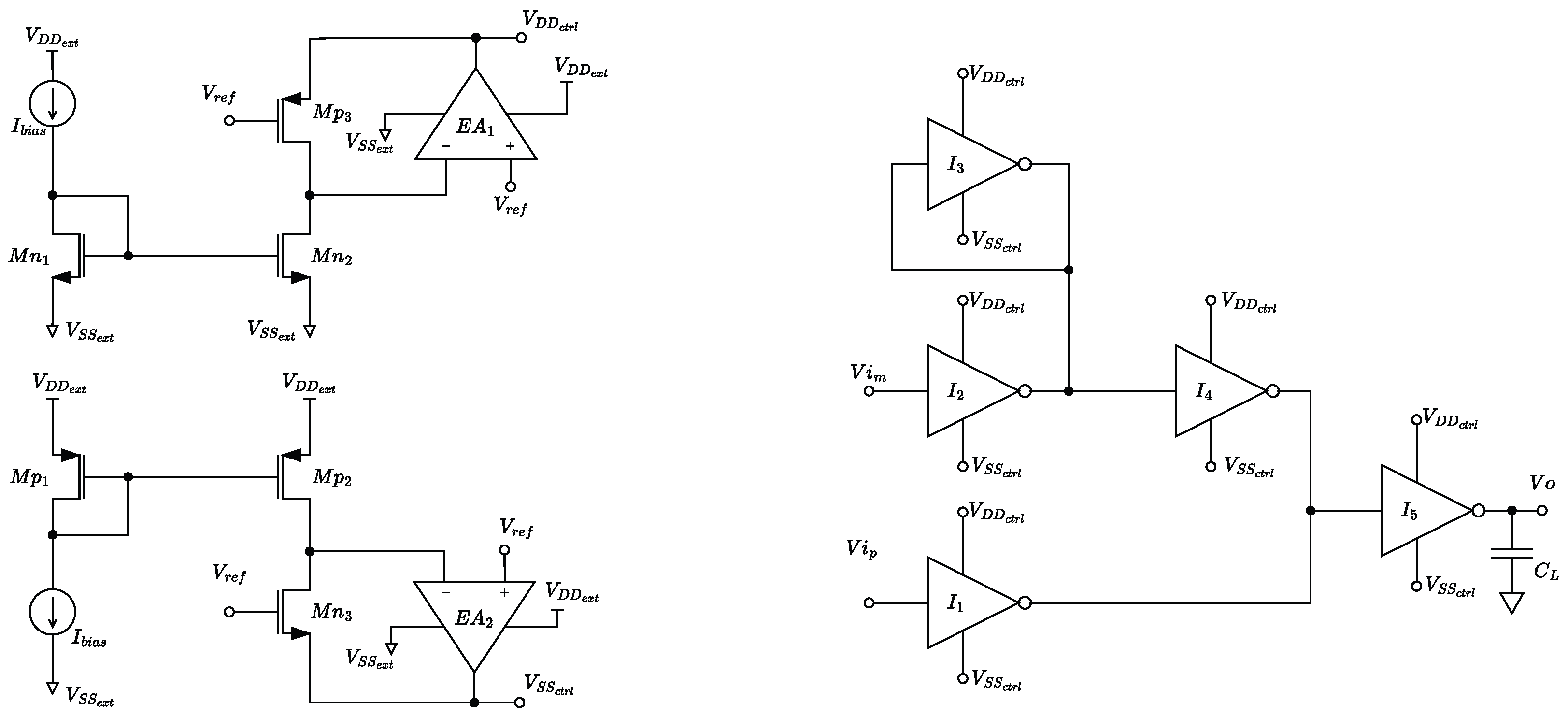
In order to properly set the quiescent current of standard-cell inverters, the approach proposed here takes advantage of two locally generated supply voltages, V D D c t r l and V S S c t r l , whose main role is to accurately set the DC current of all the standard-cell inverters used for analog design through a replica-bias approach, thus strongly reducing the variability of the transconductance and output conductance g m i and g d s i of the standard-cell inverters operating in a sub-threshold. The simplified schematic of the proposed approach to set the quiescent current of standard-cell inverter is reported in Figure 4. The two circuits in the upper and lower right corner of the figure act as ASV generators to produce the V D D c t r l and V S S c t r l , respectively. These voltages are then routed as local supply voltages to all the standard-cell inverters used for analog purposes (i.e., the inverters implementing the two-stage OTA in this example). Referring to Figure 4, transistors M n 3 and M p 3 implement a replica of the NMOS and PMOS device of the minimum area standard-cell inverter, respectively, whereas M n 1 M n 2 and M p 1 M p 2 implement conventional current mirrors that force a reference current I b i a s in M n 3 and M p 3 . The gate voltage of the replica devices M n 3 and M p 3 is set to a reference voltage V r e f (usually set at the midpoint between V D D and V S S ), and their drain voltage is compared with the same reference voltage V r e f through the two error amplifiers E A 1 and E A 2 . The task of amplifiers E A 1 and E A 2 is to generate the two control voltages, V D D c t r l and V S S c t r l , which close the loops at the source nodes of M p 3 and M n 3 , respectively. In this way, the two control voltages V D D c t r l and V S S c t r l are changed by the feedback loops in order to set the bias current of M n 3 and M p 3 to I b i a s and the drain voltages of M n 3 and M p 3 to V r e f despite PVT variations, as will be better assessed in the next sections.

3.1. Analysis of the Feedback Loop in the ASV Generators

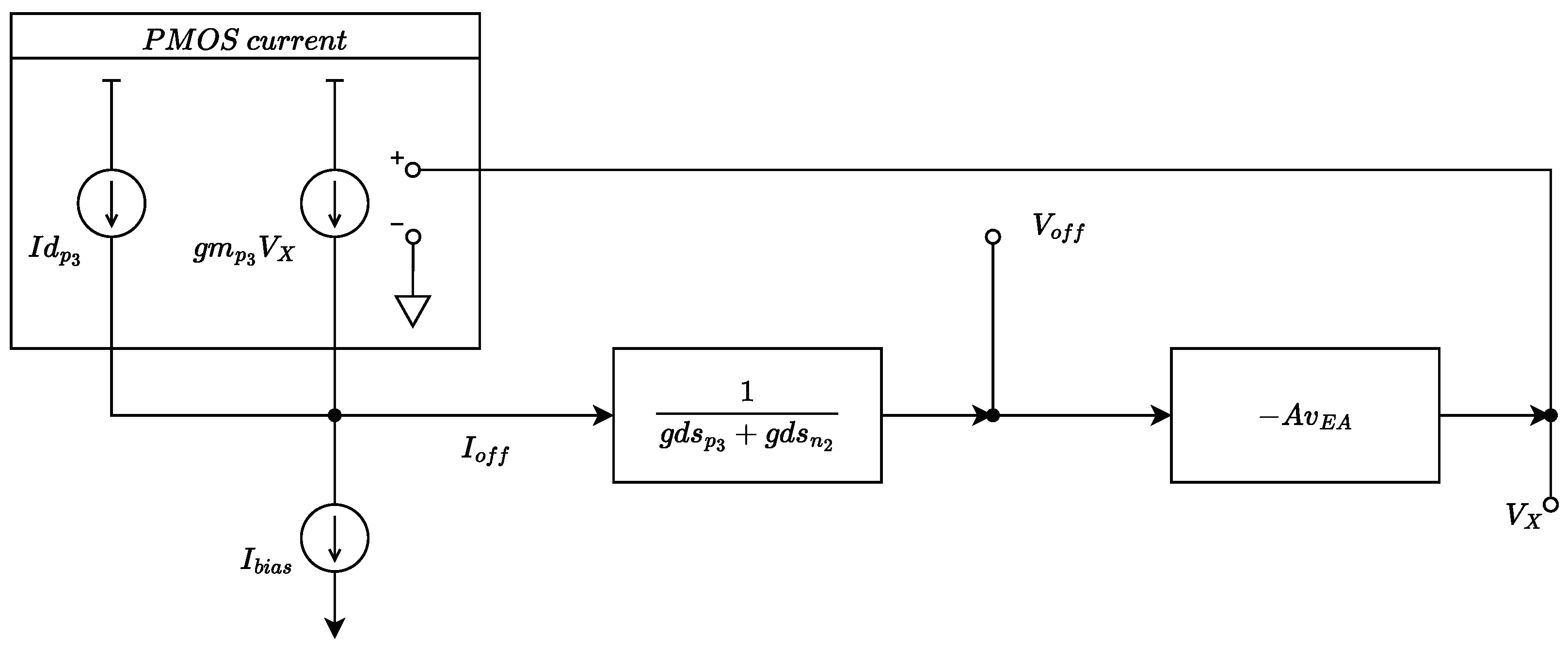
In the following section, we derive a simplified model of the feedback loop implementing the ASV generator for the V D D c t r l (see the upper right corner of Figure 4). A similar model can be developed for the ASV generator for the V S S c t r l . The block scheme derived for the feedback loop in the upper right corner of Figure 4 is depicted in Figure 5: I d p 3 is the current that flows in M p 3 when the supply voltage V D D c t r l has its nominal value, and V x is the variation of V D D c t r l with respect to such value. I b i a s is the reference current, mirrored through M n 1 , 2 .
The comparison between the drain current of M p 3 and I b i a s generates an offset current I o f f which, flowing through the output conductance g d s p 3 + g d s n 2 , turns into an offset voltage ( V o f f in Figure 5 is the difference between the DC output voltage and V r e f ). The error amplifier E A 1 , with gain A v E A , closes the loop, modifying the supply voltage V D D c t r l , hence the current in M p 3 , to cancel the offset. Due to the finite loop gain, the residual offset current is
I o f f = I d p 3 I d b i a s 1 + g m p 3 A v E A g d s p 3 + g d s n 2
By performing the same analysis on the feedback loop in the ASV generator for the V S S c t r l , the offset current in M n 3 can be expressed as follows:
I o f f = I d n 3 I d b i a s 1 + g m n 3 A v E A g d s n 3 + g d s p 2
Equations (12) and (13) show that the proposed feedback loops suppress the offset current by a factor given by the gain of the auxiliary amplifier times the gain of the replica stage. This means that the feedback loops allow us to set the quiescent current of M p 3 and of M n 3 to I b i a s , strongly reducing the effect of PVT variations (which give rise to the component I o f f ). It has to be pointed out that, since M p 3 and of M n 3 are a replica of the transistors of the standard-cell inverter, the quiescent current of all the standard-cell inverters using V D D c t r l and V S S c t r l as local supply voltages will also be set approximately equal to I b i a s despite PVT variations.

3.2. Implementation of the Error Amplifier

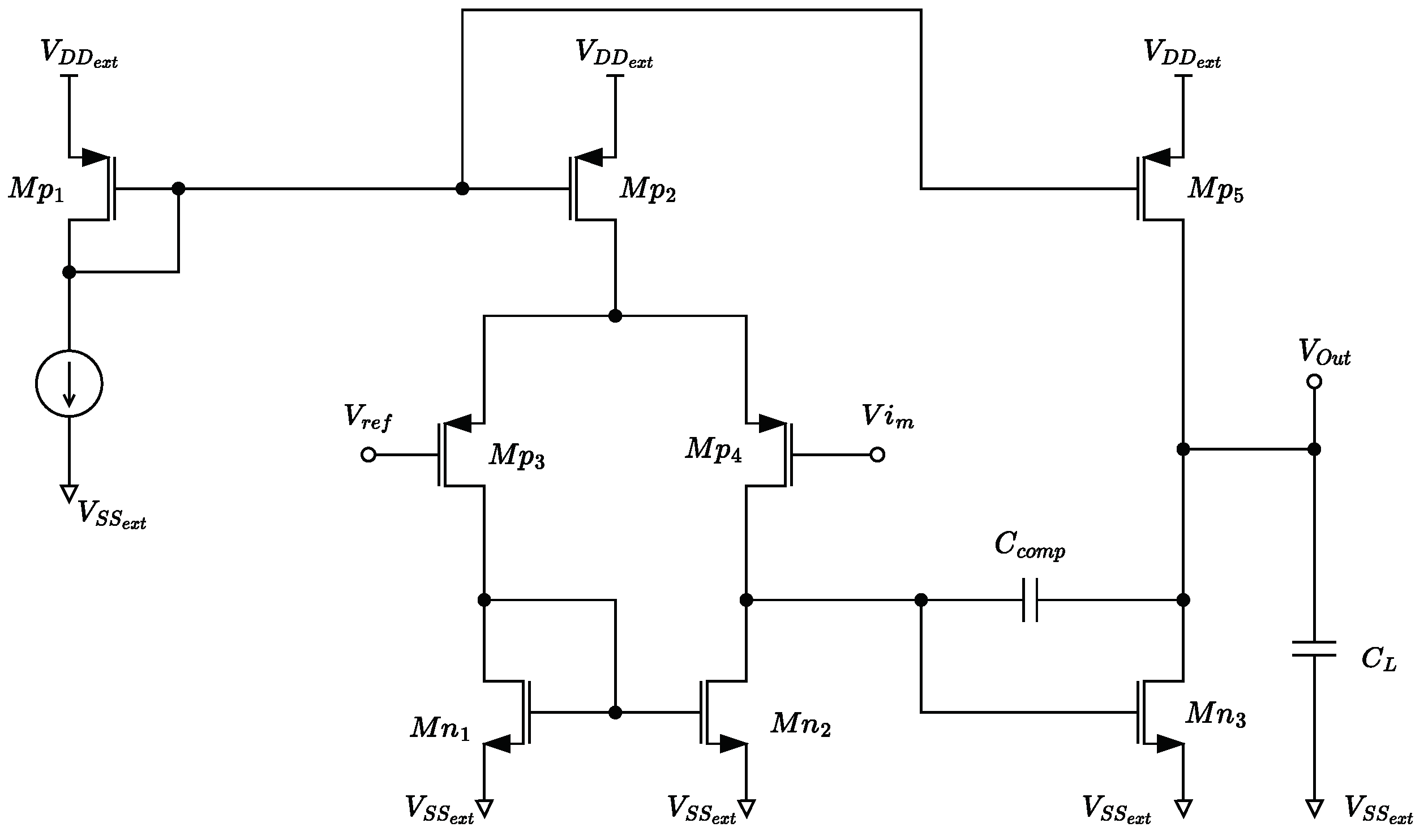
The error amplifier was implemented according to Figure 6. It is a two-stage OTA with a Miller compensation. The transistors’ sizes are reported in Table 4. Since V r e f = 0.2 V, V D D = 0.5 V, and M p 3 and M p 4 are biased in a sub-threshold, the current source M p 2 is properly biased in saturation. The compensation capacitance C c o m p is 10 pF, whereas C o E A is the parasitic capacitance seen at the output of the error amplifier, which is in the order of hundreds fF (it depends on the C g s and C g d seen at the source terminals of transistors).
To effectively bias multiple stages, it is crucial to properly size the error amplifier’s output stage, which has to supply a current to all the standard cells. In the design phase, by estimating the overall system requirements, the error amplifier can be appropriately sized to bias all cells simultaneously, eliminating the need for additional stages.

3.3. Impact of the V D D c t r l and V S S c t r l ASV Generators on the PSRR

By using the proposed approach to stabilize the bias current of standard-cell-based analog blocks, the supply voltage to such blocks is provided by the ASV generators. This affects the power supply rejection ratio (PSRR) of the analog block, since disturbances from the overall supply voltages are filtered by the ASVGs: the overall gain from the global positive supply voltage to the output of the analog block can be written as
A d d , t o t = A A S V 1 , d d A d d + A A S V 2 , d d A s s
and
A s s , t o t = A A S V 1 , s s A d d + A A S V 2 , s s A s s
where A d d and A s s are the gains from positive and negative supply voltages to the output of the analog block (e.g., an OTA), and A A S V 1 , d d ( A A S V 1 , s s ) and A A S V 2 , d d ( A A S V 2 , s s ) are the gains from the positive (negative) supply voltage to the outputs of the positive and negative (positive) ASVGs, respectively. An analog expression can be written for the negative supply voltage.
The analysis of the ASVG circuit in Figure 4 shows that the gains A A S V 1 , d d and A A S V 2 , s s are approximately inversely proportional to the intrinsic gain A 0 of MOS devices, thus resulting in an improvement of the order of A 0 in the PSRR. If we define the positive and negative PSRRs of the analog block as P S R R d and P S R R s , the overall positive and negative PSRRs are approximately given by
P S R R d t o t = A 0 1 P S R R d 1 P S R R s 1 + g m p g m n
P S R R s t o t = A 0 1 P S R R s 1 P S R R d 1 + g m n g m p
where the generic transconductance gain of MOS devices is denoted with g m p and g m n .
In Figure 7, the gain A A S V 1 , d d is reported in a blue color, gain A A S V 2 , d d is reported in a green color, gain A A S V 1 , s s is reported in a red color, and gain A A S V 2 , s s is reported in a purple color.

4. Simulation Results on the Standard-Cell-Based Two-Stage OTA Operating in Sub-Threshold with the Proposed Quiescent Current Control

The two-stage standard-cell-based OTA with the proposed quiescent current control scheme reported in Figure 4 was also designed in reference to the TSMC 180 nm CMOS technology, with a global supply voltage V D D V S S of 0.5 V for the ASV generators and a nominal local supply voltage V D D c t r l V S S c t r l of 0.35 V for the standard-cell inverters used in the OTA. Transistor-level simulations were carried out within the Cadence Virtuoso environment.
To highlight the effectiveness of the proposed approach in strongly reducing the effects of PVT variations, the same parametric and corner simulations executed for the OTA without the quiescent current control were also carried out on the OTA, exploiting the proposed current control approach. Results of these simulations are summarized in Table 5, where Itot is the total current drawn by the OTA. The first five columns in the table refer to the five process corners of the technology, the sixth and seventh columns refer to global supply voltage variations, and the last two columns refer to temperature variations. As it can be observed, with respect to the conventional OTA without quiescent current control, both current dissipation and the GBW are much more stable. To further improve the robustness of the proposed circuit to temperature variations, the reference current I b i a s was assumed to be generated by a proportional to absolute temperature (PTAT) current source, which set a bias DC in the standard-cell inverter to approximately 500 pA in typical conditions. The usage of the PTAT current source is evident from the the last two columns of Table 5, in which Itot results varied from 1.945 nA to 3.56 nA in order to keep the GBW almost constant in the specified temperature range from 0° to 80°.
In addition, the results of process-only and mismatch-only Monte Carlo simulations are reported in Table 6 and Table 7, respectively. The histograms of GBW, Pd, and m φ under process-only and mismatch-only Monte Carlo simulations are also reported in Figure 8 and Figure 9, respectively. As it can be observed, the power dissipated. Moreover, the current consumption and the GBW were characterized by an extremely small standard deviation, especially if compared with the same topology characterized without a control loop, confirming the extreme robustness achieved by the standard-cell-based OTA exploiting the proposed ASV-based quiescent current control approach.

5. Conclusions

In most cases, the existing ways to implement analog building blocks from digital standard-cell libraries do not provide enough control over the quiescent operating point. This makes the same solutions vulnerable to significant fluctuations in performance when PVT conditions are changed. This research offered a technique for biasing through the development of ASV generators, which appears to be a workable way to create analog circuits based on standard cells that have output voltages and quiescent currents that are well defined. A fully synthesizable two-stage OTA was designed in a 180 nm CMOS process to illustrate the application of the proposed approach. Excellent stability of the GBW, power consumption, and phase margin of the OTA exploiting the proposed quiescent current control strategy were demonstrated by the simulation results. More specifically, the ratio between the mean value and the standard deviation ( σ μ ) of the GBW (Pd) obtained from process-only Monte Carlo simulations for the OTA designed with the proposed approach was about 0.06 (0.017). These values, when compared with the σ μ values of the GBW (Pd) obtained from the conventional standard-cell-based OTA without ASVGs, which were 0.5 (0.53), confirm the dramatic reduction in the σ μ of main performance parameters under process variations that was allowed by the proposed approach.

Author Contributions

Conceptualization, R.D.S., G.S. and F.C.; methodology, R.D.S., G.S. and F.C.; software, R.D.S.; validation, R.D.S. and G.S.; formal analysis, R.D.S.; investigation, R.D.S. and G.S.; resources, G.S.; data curation, R.D.S.; writing—original draft preparation, R.D.S.; writing—review and editing, R.D.S., G.S. and F.C.; visualization, R.D.S., G.S. and F.C.; supervision, G.S.; project administration, G.S.; funding acquisition, G.S. All authors have read and agreed to the published version of the manuscript.

Funding

This research received no external funding.

Data Availability Statement

No new data were created or analyzed in this study. Data sharing is not applicable to this article.

Conflicts of Interest

The authors declare no conflicts of interest.

Abbreviations

The following abbreviations are used in this manuscript:
ASVAdaptive Supply Voltage
ASVGAdaptive Supply Voltage Generator
DACDigital-to-Analog Converter
DIGOTADigital Operational Transconductance Amplifier
GBWGain–Bandwidth Product
IoTInternet of Things
OTAOperational Transconductance Amplifier
PSRRPower Supply Rejection Ratio
PVTProcess, Supply Voltage, and Temperature
ULPUltra-Low Power
ULVUltra-Low Voltage

References

  1. Buzzin, A.; Asquini, R.; Caputo, D.; de Cesare, G. Sensitive and Compact Evanescent-Waveguide Optical Detector for Sugar Sensing in Commercial Beverages. Sensors 2023, 23, 8184. [Google Scholar] [CrossRef] [PubMed]
  2. Gupta, B.B.; Quamara, M. An overview of Internet of Things (IoT): Architectural aspects, challenges, and protocols. Concurr. Comput. Pract. Exper. 2020, 32, e4946. [Google Scholar] [CrossRef]
  3. Kadhim, K.T.; Alsahlany, A.M.; Wadi, S.M.; Kadhum, H.T. An Overview of Patient’s Health Status Monitoring System Based on Internet of Things (IoT). Wirel. Pers. Commun. 2020, 114, 2235–2262. [Google Scholar] [CrossRef]
  4. Barbirotta, M.; Cheikh, A.; Mastrandrea, A.; Menichelli, F.; Vigli, F.; Olivieri, M. A Fault Tolerant soft-core obtained from an Interleaved-Multi- Threading RISC- V microprocessor design. In Proceedings of the 2021 IEEE International Symposium on Defect and Fault Tolerance in VLSI and Nanotechnology Systems (DFT), Athens, Greece, 6–8 October 2021; pp. 6–8. [Google Scholar] [CrossRef]
  5. Chuah, J.W. The Internet of Things: An overview and new perspectives in systems design. In Proceedings of the 2014 International Symposium on Integrated Circuits (ISIC), Singapore, 10–12 December 2014; pp. 10–12. [Google Scholar] [CrossRef]
  6. Aiello, O.; Crovetti, P.; Alioto, M. Fully Synthesizable Low-Area Analogue-to-Digital Converters with Minimal Design Effort Based on the Dyadic Digital Pulse Modulation. IEEE Access 2020, 8, 70890–70899. [Google Scholar] [CrossRef]
  7. Di Patrizio Stanchieri, G.; Aiello, O.; De Marcellis, A. A 0.4 V 180 nm CMOS Sub-μW Ultra-Compact and Low-Effort Design PWM-Based ADC. In Proceedings of the 2024 IEEE International Symposium on Circuits and Systems (ISCAS), New Delhi, India, 18–19 October 2024; pp. 19–22. [Google Scholar] [CrossRef]
  8. Toledo, P.; Aiello, O.; Crovetti, P.S. A 300mV-Supply Standard-Cell-Based OTA with Digital PWM Offset Calibration. In Proceedings of the 2019 IEEE Nordic Circuits and Systems Conference (NORCAS): NORCHIP and International Symposium of System-on-Chip (SoC), Helsinki, Finland, 29–30 October 2019; pp. 29–30. [Google Scholar] [CrossRef]
  9. Centurelli, F.; Della Sala, R.; Scotti, G. A Standard-Cell-Based CMFB for Fully Synthesizable OTAs. J. Low Power Electron. Appl. 2022, 12, 27. [Google Scholar] [CrossRef]
  10. Barbirotta, M.; Menichelli, F.; Cheikh, A.; Mastrandrea, A.; Angioli, M.; Olivieri, M. Dynamic Triple Modular Redundancy in Interleaved Hardware Threads: An Alternative Solution to Lockstep Multi-Cores for Fault-Tolerant Systems. IEEE Access 2024, 12, 95720–95735. [Google Scholar] [CrossRef]
  11. Sood, L.; Agarwal, A. A CMOS standard-cell based fully-synthesizable low-dropout regulator for ultra-low power applications. AEU Int. J. Electron. Commun. 2021, 141, 153958. [Google Scholar] [CrossRef]
  12. Xu, Z.; Ojima, N.; Li, S.; Iizuka, T. An All-Standard-Cell-Based Synthesizable SAR ADC With Nonlinearity-Compensated RDAC. IEEE Trans. Very Large Scale Integr. VLSI Syst. 2021, 29, 2153–2162. [Google Scholar] [CrossRef]
  13. Toledo, P.; Crovetti, P.; Aiello, O.; Alioto, M. Design of Digital OTAs With Operation Down to 0.3 V and nW Power for Direct Harvesting. IEEE Trans. Circuits Syst. I 2021, 68, 3693–3706. [Google Scholar] [CrossRef]
  14. Toledo, P.; Crovetti, P.; Aiello, O.; Alioto, M. Fully Digital Rail-to-Rail OTA With Sub-1000-μm2 Area, 250-mV Minimum Supply, and nW Power at 150-pF Load in 180 nm. IEEE Solid-State Circuits Lett. 2020, 3, 474–477. [Google Scholar] [CrossRef]
  15. Aiello, O.; Crovetti, P.; Sharma, A.; Alioto, M. Fully-Synthesizable Current-Input ADCs for Ultra-Low Area and Minimal Design Effort. In Proceedings of the 2019 26th IEEE International Conference on Electronics, Circuits and Systems (ICECS), Genoa, Italy, 27–29 November 2019; pp. 27–29. [Google Scholar] [CrossRef]
  16. Liu, J.; Park, B.; Guzman, M.; Fahmy, A.; Kim, T.; Maghari, N. A Fully Synthesized 77-dB SFDR Reprogrammable SRMC Filter Using Digital Standard Cells. IEEE Trans. Very Large Scale Integr. VLSI Syst. 2018, 26, 1126–1138. [Google Scholar] [CrossRef]
  17. Toledo, P.; Klimach, H.; Bampi, S.; Crovetti, P. A 300 mV-Supply, 144 nW-Power, 0.03 mm2-Area, 0.2-PEF Digital-Based Biomedical Signal Amplifier in 180 nm CMOS. In Proceedings of the 2021 IEEE International Symposium on Medical Measurements and Applications (MeMeA), Lausanne, Switzerland, 23–25 June 2021; pp. 23–25. [Google Scholar] [CrossRef]
  18. Della Sala, R.; Centurelli, F.; Scotti, G. A High Performance 0.3 V Standard-Cell-Based OTA Suitable for Automatic Layout Flow. Appl. Sci. 2023, 13, 5517. [Google Scholar] [CrossRef]
  19. Sala, R.D.; Centurelli, F.; Scotti, G. A Novel Differential to Single-Ended Converter for Ultra-Low-Voltage Inverter-Based OTAs. IEEE Access 2022, 10, 98179–98190. [Google Scholar] [CrossRef]
  20. Toledo, P.; Crovetti, P.; Klimach, H.; Bampi, S.; Aiello, O.; Alioto, M. A 300mV-Supply, Sub-nW-Power Digital-Based Operational Transconductance Amplifier. IEEE Trans. Circuits Syst. II 2021, 68, 3073–3077. [Google Scholar] [CrossRef]
  21. Angioli, M.; Barbirotta, M.; Cheikh, A.; Mastrandrea, A.; Menichelli, F.; Jamili, S.; Olivieri, M. Design, Implementation and Evaluation of a New Variable Latency Integer Division Scheme. IEEE Trans. Comput. 2024, 73, 1767–1779. [Google Scholar] [CrossRef]
  22. Privitera, M.; Crovetti, P.; Grasso, A.D. A Novel Digital OTA Topology With 66-dB DC Gain and 12.3-kHz Bandwidth. IEEE Trans. Circuits Syst. II 2023, 70, 3988–3992. [Google Scholar] [CrossRef]
  23. Crovetti, P.S. All-Digital High Resolution D/A Conversion by Dyadic Digital Pulse Modulation. IEEE Trans. Circ. Syst. I 2016, 64, 573–584. [Google Scholar] [CrossRef]
  24. Aiello, O.; Crovetti, P.; Alioto, M. Standard Cell-Based Ultra-Compact DACs in 40-nm CMOS. IEEE Access 2019, 7, 126479–126488. [Google Scholar] [CrossRef]
  25. Aiello, O.; Crovetti, P.S.; Alioto, M. Fully Synthesizable Low-Area Digital-to-Analog Converter With Graceful Degradation and Dynamic Power-Resolution Scaling. IEEE Trans. Circ. Syst. I 2019, 66, 2865–2875. [Google Scholar] [CrossRef]
  26. Rubino, R.; Crovetti, P.S.; Aiello, O. Design of Relaxation Digital-to-Analog Converters for Internet of Things Applications in 40nm CMOS. In Proceedings of the 2019 IEEE Asia Pacific Conference on Circuits and Systems (APCCAS), Bangkok, Thailand, 11–14 November 2019; pp. 11–14. [Google Scholar] [CrossRef]
  27. Sala, R.D.; Centurelli, F.; Scotti, G. Enabling ULV Fully Synthesizable Analog Circuits: The BA Cell, a Standard-Cell-Based Building Block for Analog Design. IEEE Trans. Circuits Syst. II 2022, 69, 4689–4693. [Google Scholar] [CrossRef]
  28. Sala, R.D.; Centurelli, F.; Scotti, G. A Novel High Performance Standard-Cell Based ULV OTA Exploiting an Improved Basic Amplifier. IEEE Access 2024, 12, 17513–17521. [Google Scholar] [CrossRef]
  29. Aiello, O.; Crovetti, P.; Alioto, M. Ultra-Low Power and Minimal Design Effort Interfaces for the Internet of Things: Invited paper. In Proceedings of the 2019 IEEE International Circuits and Systems Symposium (ICSyS), Kuantan, Malaysia, 18–19 September 2019; pp. 18–19. [Google Scholar] [CrossRef]
  30. Buzzin, A.; Cupo, S.; Giovine, E.; de Cesare, G.; Belfiore, N.P. Compliant Nano-Pliers as a Biomedical Tool at the Nanoscale: Design, Simulation and Fabrication. Micromachines 2020, 11, 1087. [Google Scholar] [CrossRef] [PubMed]
  31. Namdari, A.; Aiello, O.; Caviglia, D.D. 0.5V 32nW Inverter-Based Gm-C Filter for Bio-Signal Processing. In Proceedings of the 2024 IEEE International Symposium on Circuits and Systems (ISCAS), New Delhi, India, 18–19 October 2024; pp. 19–22. [Google Scholar] [CrossRef]
  32. Sanchotene Silva, R.; Rodovalho, L.H.; Aiello, O.; Ramos Rodrigues, C. A 1.9 nW, Sub-1 V, 542 pA/V Linear Bulk-Driven OTA with 154 dB CMRR for Bio-Sensing Applications. J. Low Power Electron. Appl. 2021, 11, 40. [Google Scholar] [CrossRef]
  33. Aiello, O.; Crovetti, P.; Lin, L.; Alioto, M. A pW-Power Hz-Range Oscillator Operating With a 0.3–1.8-V Unregulated Supply. IEEE J. Solid-State Circuits 2019, 54, 1487–1496. [Google Scholar] [CrossRef]
  34. Buzzin, A.; Asquini, R.; Caputo, D.; de Cesare, G. Evanescent waveguide lab-on-chip for optical biosensing in food quality control. Photonics Res. 2022, 10, 1453–1461. [Google Scholar] [CrossRef]
  35. Aiello, O. Electromagnetic Susceptibility of Battery Management Systems’ ICs for Electric Vehicles: Experimental Study. Electronics 2020, 9, 510. [Google Scholar] [CrossRef]
  36. Aiello, O.; Crovetti, P.; Alioto, M. 5.2 Capacitance-to-Digital Converter for Operation Under Uncertain Harvested Voltage down to 0.3V with No Trimming, Reference and Voltage Regulation. In Proceedings of the 2021 IEEE International Solid-State Circuits Conference (ISSCC), San Francisco, CA, USA, 13–22 February 2021; pp. 13–22. [Google Scholar] [CrossRef]
  37. Rodovalho, L.H.; Aiello, O.; Rodrigues, C.R. Ultra-Low-Voltage Inverter-Based Operational Transconductance Amplifiers with Voltage Gain Enhancement by Improved Composite Transistors. Electronics 2020, 9, 1410. [Google Scholar] [CrossRef]
  38. Ballo, A.; Grasso, A.D.D.; Pennisi, S.; Susinni, G. A 0.3-V 8.5-μ a Bulk-Driven OTA. IEEE Trans. Very Large Scale Integr. VLSI Syst. 2023, 31, 1444–1448. [Google Scholar] [CrossRef]
  39. Ballo, A.; Carvajal, R.G.; Grasso, A.D.; Luján-Martínez, C.I.; Pennisi, S.; Venezia, C. 0.35-V SR-Enhanced Bulk-Driven OTA for Loads up to 10 nF. IEEE Trans. Circ. Syst. I 2024, 1–9. [Google Scholar] [CrossRef]
  40. Della Sala, R.; Centurelli, F.; Monsurró, P.; Scotti, G. On the Feasibility of Cascode and Regulated Cascode Amplifier Stages in ULV Circuits Exploiting MOS Transistors in Deep Subthreshold Operation. IEEE Access 2024, 12, 73292–73303. [Google Scholar] [CrossRef]
  41. Kumngern, M.; Aupithak, N.; Khateb, F.; Kulej, T. 0.5 V Fifth-Order Butterworth Low-Pass Filter Using Multiple-Input OTA for ECG Applications. Sensors 2020, 20, 7343. [Google Scholar] [CrossRef] [PubMed]
  42. Khateb, F.; Kulej, T.; Vlassis, S. Extremely Low-Voltage Bulk-Driven Tunable Transconductor. Circuits Syst. Signal Process. 2017, 36, 511–524. [Google Scholar] [CrossRef]
  43. Kulej, T.; Khateb, F.; Arbet, D.; Stopjakova, V. A 0.3-V High Linear Rail-to-Rail Bulk-Driven OTA in 0.13 μm CMOS. IEEE Trans. Circuits Syst. II 2022, 69, 2046–2050. [Google Scholar] [CrossRef]
  44. Jaikla, W.; Khateb, F.; Kumngern, M.; Kulej, T.; Ranjan, R.K.; Suwanjan, P. 0.5 V Fully Differential Universal Filter Based on Multiple Input OTAs. IEEE Access 2020, 8, 187832–187839. [Google Scholar] [CrossRef]
  45. Rodovalho, L.H.; Ramos Rodrigues, C.; Aiello, O. Self-Biased and Supply-Voltage Scalable Inverter-Based Operational Transconductance Amplifier with Improved Composite Transistors. Electronics 2021, 10, 935. [Google Scholar] [CrossRef]
  46. Kulej, T. 0.5-V bulk-driven CMOS operational amplifier. IET Circuits Devices Syst. 2013, 7, 352–360. [Google Scholar] [CrossRef]
  47. Kulej, T.; Khateb, F. Design and implementation of sub 0.5-V OTAs in 0.18-μm CMOS. Int. J. Circuit Theory Appl. 2018, 46, 1129–1143. [Google Scholar] [CrossRef]
  48. Kulej, T.; Khateb, F. A Compact 0.3-V Class AB Bulk-Driven OTA. IEEE Trans. Very Large Scale Integr. VLSI Syst. 2019, 28, 224–232. [Google Scholar] [CrossRef]
  49. Kulej, T.; Khateb, F. A 0.3-V 98-dB rail-to-rail OTA in 0.18 μm CMOS. IEEE Access 2020, 8, 27459–27467. [Google Scholar] [CrossRef]
  50. Khateb, F.; Kulej, T. Design and Implementation of a 0.3-V Differential Difference Amplifier. IEEE Trans. Circ. Syst. I 2018, 66, 513–523. [Google Scholar] [CrossRef]
  51. Della Sala, R.; Centurelli, F.; Monsurrò, P.; Scotti, G.; Trifiletti, A. A 0.3V rail-to-rail three-stage OTA with high DC gain and improved robustness to PVT variations. IEEE Access 2023, 11, 19635–19644. [Google Scholar] [CrossRef]
  52. Kulej, T.; Khateb, F. 0.4-V bulk-driven differential-difference amplifier. Microelectron. J. 2015, 46, 362–369. [Google Scholar] [CrossRef]
  53. Kulej, T. 0.4-V bulk-driven operational amplifier with improved input stage. Circuits Syst. Signal Process. 2015, 34, 1167–1185. [Google Scholar] [CrossRef]
  54. Kulej, T. 0.5-V bulk-driven OTA and its applications. Int. J. Circuit Theory Appl. 2015, 43, 187–204. [Google Scholar] [CrossRef]
  55. Khateb, F.; Kulej, T.; Akbari, M.; Steffan, P. 0.3-V bulk-driven nanopower OTA-C integrator in 0.18 μm CMOS. Circuits Syst. Signal Process. 2019, 38, 1333–1341. [Google Scholar] [CrossRef]
  56. Centurelli, F.; Della Sala, R.; Monsurró, P.; Scotti, G.; Trifiletti, A. A novel OTA architecture exploiting current gain stages to boost bandwidth and slew-rate. Electronics 2021, 10, 1638. [Google Scholar] [CrossRef]
  57. Della Sala, R.; Spinogatti, V.; Bocciarelli, C.; Centurelli, F.; Trifiletti, A. A 0.15-to-0.5 V Body-Driven Dynamic Comparator with Rail-to-Rail ICMR. J. Low Power Electron. Appl. 2023, 13, 35. [Google Scholar] [CrossRef]
  58. Aiello, O.; Crovetti, P.; Toledo, P.; Alioto, M. Rail-to-Rail Dynamic Voltage Comparator Scalable Down to pW-Range Power and 0.15-V Supply. IEEE Trans. Circuits Syst. II 2021, 68, 2675–2679. [Google Scholar] [CrossRef]
  59. Sala, R.D.; Centurelli, F.; Scotti, G.; Palumbo, G. Rail to Rail ICMR and High Performance ULV Standard-Cell-Based Comparator for Biomedical and IoT Applications. IEEE Access 2024, 12, 4642–4659. [Google Scholar] [CrossRef]
  60. Sala, R.D.; Bocciarelli, C.; Centurelli, F.; Spinogatti, V.; Trifiletti, A. A Novel Ultra-Low Voltage Fully Synthesizable Comparator exploiting NAND Gates. In Proceedings of the 2023 18th Conference on Ph.D Research in Microelectronics and Electronics (PRIME), Valencia, Spain, 18–21 June 2023; pp. 18–21. [Google Scholar] [CrossRef]
  61. Aiello, O.; Crovetti, P.; Alioto, M. Fully Synthesizable, Rail-to-Rail Dynamic Voltage Comparator for Operation down to 0.3 V. In Proceedings of the 2018 IEEE International Symposium on Circuits and Systems (ISCAS), Florence, Italy, 27–30 May 2018; pp. 27–30. [Google Scholar] [CrossRef]
  62. Ballo, A.; Pennisi, S.; Scotti, G. 0.5 V CMOS Inverter-Based Transconductance Amplifier with Quiescent Current Control. J. Low Power Electron. Appl. 2021, 11, 37. [Google Scholar] [CrossRef]
  63. Chen, T.; Naffziger, S. Comparison of adaptive body bias (ABB) and adaptive supply voltage (ASV) for improving delay and leakage under the presence of process variation. IEEE Trans. Very Large Scale Integr. VLSI Syst. 2003, 11, 888–899. [Google Scholar] [CrossRef]
  64. Eireiner, M.; Henzler, S.; Georgakos, G.; Berthold, J.; Schmitt-Landsiedel, D. Local Supply Voltage Adjustment for Low Power Parametric Yield Increase. In Proceedings of the 2006 32nd European Solid-State Circuits Conference, Montreux, Switzerland, 19–21 September 2006; pp. 98–101. [Google Scholar] [CrossRef]
  65. Cha, S.; Milor, L. Adaptive supply voltage and duty cycle controller for yield-power optimization of ICs. In Proceedings of the 2017 7th IEEE International Workshop on Advances in Sensors and Interfaces (IWASI), Vieste, Italy, 15–16 June 2017; pp. 133–138. [Google Scholar] [CrossRef]
  66. Nielsen, L.S.; Niessen, C.; Sparso, J.; van Berkel, K. Low-power operation using self-timed circuits and adaptive scaling of the supply voltage. IEEE Trans. Very Large Scale Integr. VLSI Syst. 1994, 2, 391–397. [Google Scholar] [CrossRef]
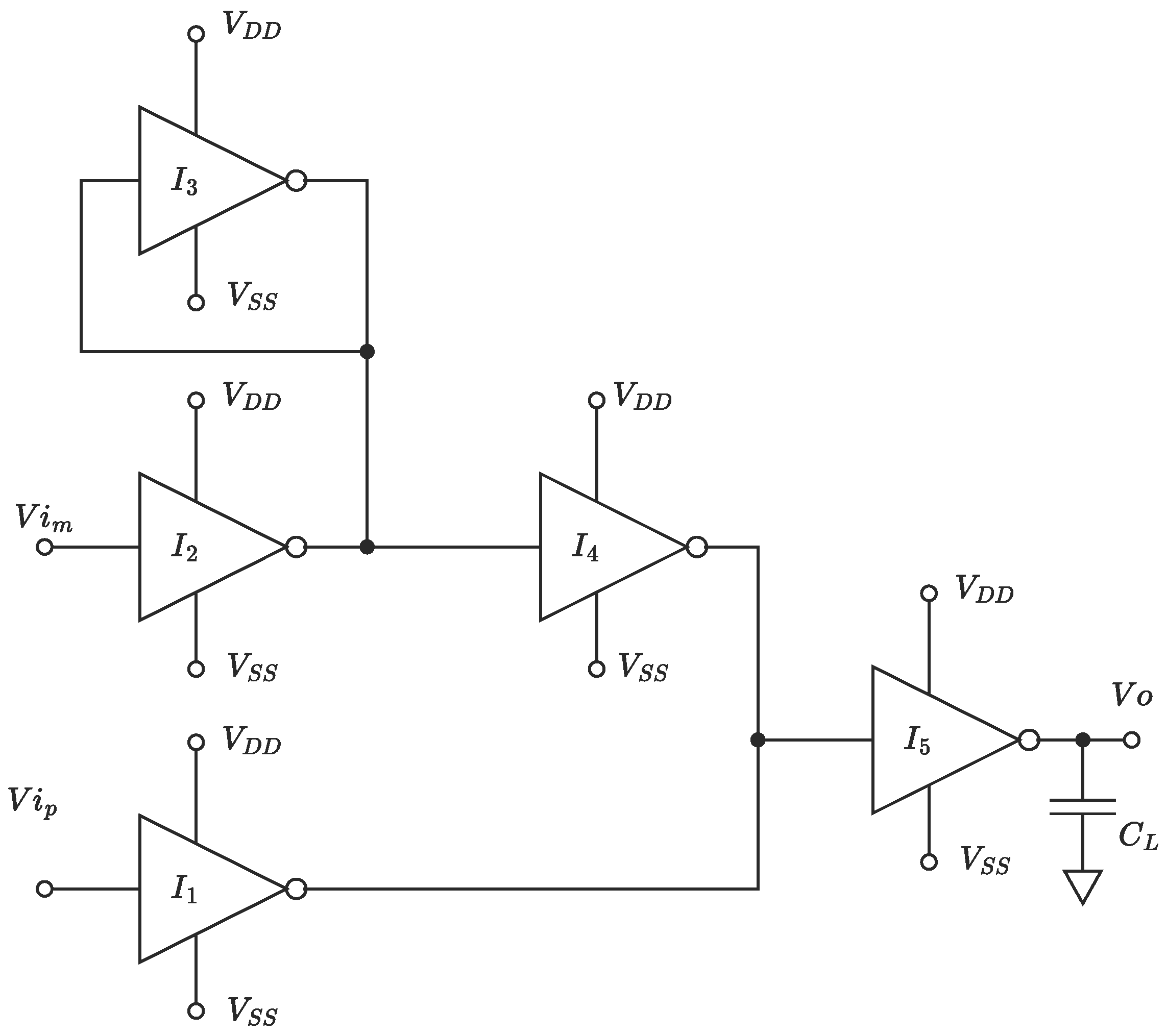
Figure 1. Conventional two-stage standard-cell-based OTA.
Jlpea 14 00039 g001
Figure 2. Gain–bandwidth product (a), power consumption (b), and phase margin (c) of the conventional standard-cell-based OTA under process-only Monte Carlo simulations.
Jlpea 14 00039 g002
Figure 3. Gain–bandwidth product (a), power consumption (b), and phase margin (c) of the conventional standard-cell-based OTA under mismatch-only Monte Carlo simulations.
Jlpea 14 00039 g003
Figure 4. Proposed approach to set the quiescent current of standard-cell inverters and application to the standard-cell-based two-stage OTA.
Jlpea 14 00039 g004
Figure 5. Block scheme derived for the feedback loop of the V D D c t r l ASV generator.
Jlpea 14 00039 g005
Figure 6. Schematic of the error amplifier.
Jlpea 14 00039 g006
Figure 7. Gain A A S V 1 , d d is reported in a blue color, gain A A S V 2 , d d is reported in a green color, gain A A S V 1 , s s is reported in a red color, and gain A A S V 2 , s s is reported in a purple color.
Jlpea 14 00039 g007
Figure 8. Gain–bandwidth product (a), power consumption (b), and phase margin (c) of the standard-cell-based OTA with the proposed quiescent current control scheme under process-only Monte Carlo simulations.
Jlpea 14 00039 g008
Figure 9. Gain–bandwidth product (a), power consumption (b), and phase margin (c) of the standard-cell-based OTA with the proposed quiescent current control scheme under mismatch-only Monte Carlo simulations.
Jlpea 14 00039 g009
Table 1. Performance parameters of the conventional standard-cell-based OTA under PVT variations.
TypFFSSSFFS90% V DD 110% V DD 80°
V o f f [mV]2.222.3−0.57.17.62.92.22.2
Pd [nW]1.6886.9580.3711.5993.3381.0131.5050.5369.713
Itot [nA]4.22117.390.9273.9988.3453.2173.9091.34124.28
A v d [dB]52.1249.5356.4151.9551.1848.7151.7852.950.55
GBW [kHz]53.56217.812.1266.6339.5813.3242.2218.05265.8
m φ [deg]60.4163.0356.3853.6771.7172.8963.9260.960.46
S R a v g [V/ms]144.5546.234.17149.5394.121.59101.190.86368.1
Table 2. Performance parameters of the conventional standard-cell-based OTA under process-only Monte Carlo simulations.
MeanStd Dev
V o f f [mV]2.30.99
Pd [nW]1.920.92
Itot [nA]4.3792.319
A v d [dB]51.120.90
m φ [deg]60.974.34
GBW [kHz]58.5326.77
S R a v g [V/ms]147.580.44
Table 3. Performance parameters of the conventional standard-cell-based OTA under mismatch-only Monte Carlo simulations.
MeanStd Dev
V o f f [mV]3.118.11
Pd [nW]1.820.44
Itot [nA]4.3141.106
A v d [dB]49.1110.11
m φ [deg]62.8910.03
GBW [kHz]56.1612.61
S R a v g [V/ms]14630.52
Table 4. Transistor sizing of the error amplifier.
Mp 1 = Mp 2 Mp 3 = Mp 4 Mn 1 = Mn 2 Mn 3 Mp 5
W [m]1 µ1 µ440 n3.52 µ4 µ
L [m]500 n500 n1 µ220 n500 n
Table 5. Performance parameters of the standard-cell-based OTA with the proposed quiescent current control scheme under PVT variations.
TypFFSSSFFS90% V DD 110% V DD 080
V o f f [mV]0.010.040.2−0.10.0230.020.130.040.03
Itot [nA]2.4972.5052.1672.3992.4992.4772.4991.9453.56
Pd [nW]1.2491.2531.0841.1991.2491.2391.250.9721.78
A v d [dB]51.2945.7258.6551.1950.7251.2751.2953.5945.41
m φ [deg]57.869.840.795859.1257.8357.8252.7569.71
GBW [kHz]33.6727.4236.0431.9133.4833.4233.6831.2531.42
S R a v g [V/ms]30.112.27114.619.2755.4133.8329.3270.827.218
Table 6. Performance parameters of the standard-cell-based OTA with the proposed quiescent current control scheme under process-only Monte Carlo simulations.
MeanStd Dev
V o f f [mV]0.030.022
Pd [nW]1.2480.022
Itot [nA]2.4970.044
A v d [dB]51.221.90
m φ [deg]58.184.31
GBW [kHz]33.412.03
S R a v g [V/ms]31.4910.48
Table 7. Performance parameters of the standard-cell-based OTA with the proposed quiescent current control scheme under mismatch-only Monte Carlo simulations.
MeanStd Dev
V o f f [mV]−0.915.82
Pd [nW]1.320.14
Itot [nA]2.620.27
A v d [dB]51.322.54
m φ [deg]58.327.30
GBW [kHz]34.699.83
S R a v g [V/ms]31.8810.48
Disclaimer/Publisher’s Note: The statements, opinions and data contained in all publications are solely those of the individual author(s) and contributor(s) and not of MDPI and/or the editor(s). MDPI and/or the editor(s) disclaim responsibility for any injury to people or property resulting from any ideas, methods, instructions or products referred to in the content.