Article

Split-Voltage Configuration Improves Integrated Amplifier Power-Efficiency

Department of Electrical and Information Engineering, Kiel University, 24143 Kiel, Germany
*
Author to whom correspondence should be addressed.
J. Low Power Electron. Appl. 2024, 14(3), 45; https://doi.org/10.3390/jlpea14030045
Submission received: 24 July 2024 / Revised: 26 August 2024 / Accepted: 2 September 2024 / Published: 4 September 2024

Abstract

:
A split-voltage amplifier architecture is proposed which improves the power efficiency compared to a conventional implementation. The approach is verified with a prototype fabricated in 0.35 µm CMOS technology using lateral bipolar input transistors. It achieves a measured DC gain of 105 V/V, a differential AC gain of 40.3 dB with a bandwidth of 55 kHz, a CMRR of approximately 75 dB, and a PSRR of 55 dB. The input-referred noise is 7 nV/√Hz and 923 nVrms integrated from 100 Hz to 10 kHz, resulting in a Noise Efficiency Factor (NEF) of 2.84 and a Power Efficiency Factor (PEF) of 18.3. The split-voltage configuration improves power efficiency by nearly 25% compared to a full voltage supply and maintains a small area design. Action potentials of the medial and lateral giant fiber of an earthworm are recorded as an example application.

1. Introduction

Amplifiers, serving as the input stage in various sensing applications, play a crucial role in determining the overall system efficiency and signal integrity. The trade-off between low-noise performance, power consumption, and circuit size remains a challenging engineering task. The input stage, essential for maintaining low noise levels, demands a relatively high supply current to achieve high transconductance ratios that ensure optimal input-referred noise (IRN). It is the power consumption of the input stage that frequently dominates the overall power of a sub-system [1]. Conversely, the output stage, when used to drive only large resistive loads with small capacitance as is typical in an integrated circuit, is considerably less current dependent but requires a higher supply voltage to seamlessly interface with subsequent circuit blocks, e.g., an on-chip analog-to-digital converter. In this context, we propose the split-voltage architecture as an approach to realize the balance between low-noise performance and power efficiency, especially for battery-operated systems. Using different supply voltage levels in a system composed of several circuit blocks is an established approach to operating each block in its optimum supply range [2]. Here, we propose to apply this principle to the individual sub-circuit level of the front-end amplifier. By providing a lower supply voltage to the input stage and a higher voltage to the output stage, the power efficiency is optimized without sacrificing the noise performance or the output voltage range. The goal here is different from power amplifiers that are used in audio amplification and similar applications and that are optimized to deliver a high output power. For example, Class-G amplifiers employ multiple supply voltages and dynamically switch between them to yield the required instantaneous output voltage with minimum power loss [3]. Conversely, in the target case of this paper, the output voltage is constant and set by the demands of the circuits following the input amplifier and it is the input stage that dominates the power loss due to its high currents demanded mainly by noise constraints. The proposed technique combines the design simplicity of a conventional linear amplifier with low power and good noise efficiency in a small area implementation suitable for CMOS integration. It maintains the independence of the main design parameters, giving the designer the freedom to optimize for a desired specification as in the original design.
Alternative solutions for achieving a favorable power-noise-trade-off have been reported. These include the current-reuse topology [4] and stacked input stages [5]. Albeit these approaches have shown to yield excellent performance with careful design, their implementation is complex and requires considerable area overhead. The split-voltage approach initially discussed in [6] retains the simple design procedure. For example, in the circuit presented here, this enables using lateral bipolar transistors as the input devices, resulting in low flicker-noise contribution, and it allows for applying the principle to a large number of parallel channels without design change (i.e., placing identical split-voltage amplifiers in parallel), where the current-reuse approach is practically limited to a few stackable channels.
Application examples include the recording of signals from freely moving animals, e.g., the electrocardiogram (ECG) [7], neural behaviors [8], and neural recording [9,10,11,12,13,14,15,16]. Considering that the biomedical signals to be measured exhibit amplitudes in the order of only a few microvolts or less, a gain exceeding 60 dB is typically required to allow the acquisition of action potentials (APs), local field potentials, and comparable biopotentials. Simultaneously, depending on the signal type, the amplifier should exhibit an integrated IRN of less than 10 µVrms [17]. Additionally, to facilitate extended measurements with battery-powered devices, there is a strong need for minimized power consumption.
Although the principle of the split-voltage amplifier is more generally applicable, this paper discusses its use by means of an example configuration for the recording of AP, as shown in Figure 1. A pair of split-voltage amplifiers is connected via electrodes and optional coupling capacitors to tissue in which APs are conducted and the resulting membrane potentials are recorded. Power is supplied by two coin cell batteries, where the capacity of the topmost cell (cell 1) is larger than that of the bottom cell (cell 2), symbolized by the parallel connection in Figure 1. Further processing of the amplified signal is not part of this paper. Analysis of the split-voltage architecture of the individual amplifier is presented in Section 2, and measurement results of a prototype amplifier realized in a 0.35 µm CMOS technology in Section 3. The application of this amplifier in recording the AP of an earthworm is demonstrated, validating its potential for real-world biological signal acquisition scenarios. A comparison with other low-noise amplifiers is provided in Section 4, followed by conclusions in Section 5.

2. Split-Voltage Amplifier Design

The proposed split-voltage amplifier consists of an input stage employing bipolar transistors, a current mirror, and a trans-impedance stage, forming a push-pull amplifier configuration. As depicted in Figure 2a, different from the conventional design, the input stage is operated with the reduced power supply voltage Vsplit. Assuming that the amplifier provides high gain, the differential voltage applied at the input nodes is small, so a low supply is not a limiting factor for this part of the circuit. To maintain the full voltage swing at the output, the output stage is powered by the lower chip supply voltage VSS. This configuration reduces the power consumption in the input stage, which in low-power amplifiers requires a large proportion of the overall power [1], without necessitating redesign of subsequent stages (e.g., an ADC) to also operate at a reduced voltage. Table 1 provides the dimensions of the transistors used here in the implementation of Figure 2a. Lateral bipolar transistors are used for Q1Q3, which can be implemented in conventional CMOS technology without a dedicated bipolar option. Despite providing the very good flicker-noise performance of a BJT, their transconductance efficiency is low, resulting in limited amplifier open-loop voltage gain (about 60 dB). The gain could be increased by cascading a second gain stage. However, in the targeted application, the amplifier linearity is not critical, so the single-stage amplifier is operated in an open-loop configuration and maximum gain to yield its optimum noise efficiency [18].
A current mirror (M1 and M2 here with a mirror ratio of 1 to 10) is assumed for generating Ibias. The maximum Vsplit voltage is determined by (1), based on the required saturation voltages of the individual transistors in the input stage:
V split _ max = V DD V GS _ M 3 , M 5 V CE _ sat V DS _ M 2
where VDS_M2 is the MOSFET saturation voltage given by (2ID/[K’W/L])½ and VGS_M3,M5 is the gate-source voltage (2ID/[K’W/L])½ + VT. The aspect ratio of M2 is designed to be large to achieve a small VDS_M2 to reduce the overall Vsplit_max. All MOS transistors are designed with a relatively large gate area to keep their flicker-noise contribution low. To maintain the bipolar input transistors in the active region, a minimum of several thermal voltages is required; in this case, 100 mV is assumed for VCE_sat. With the given W/L-ratios in Table 1, Ibias set to 3 µA, and a process-dependent parameter K′ of approximately 210 µA/V2 (NMOS) and 45 µA/V2 (PMOS with VT of 0.65 V), the transistor voltages are calculated and also given in Table 1. They result in Vsplit_max of 2.0 V with reference to VSS. However, this value is approximate and does not account for process variations, so a lower voltage should be selected in practice.
The selected voltage Vsplit also affects the available input common-mode (CM) range VCM with its lowest and highest voltage, respectively, given by
V CM _ min = V split + V BE + V D S M 2
V CM _ max = V DD V G S M 3 , 5 + V BE V CE _ sat
Expression (2) shows that the CM input level must be higher than Vsplit. This denies the use of evenly split supply voltages if a half-voltage ground is desired for the CM reference. However, in many applications—as the one presented here—the CM level may be chosen liberally and enables the convenient use of dual battery supplies. Here, it is proposed to use a pair of 1.5 V batteries connected in series to provide VDD. The connection point yields Vsplit. Solving (2) and (3) then yields a minimum CM level of 2.2 V and a maximum of 2.7 V. A higher maximum level could be realized by using low-voltage mirrors instead of the simple PMOS mirrors employed here. Due to its configuration, one of the batteries (here, the one for the higher voltage, cell 1) supplies more current and hence depletes faster than the other one. This is offset by employing a bottom-side battery with half the capacity, which further reduces the system’s weight and size. Here, SR44 (165 mAh, 2.11 g, 11.5 × 5.4 mm) and SR54 (81 mAh, 1.28 g, 11.5 × 3 mm) type coin cells are used. Clearly, other means of providing dual supply voltages are possible in principle. Voltage or power converters that are conventionally used in multi-chip systems could be employed. However, they require additional design effort and, more importantly, have limited efficiency, typically ranging from about 75% to 95% depending on the implementation. The power lost in conversion partially offsets the power saving of the split-voltage approach. Direct battery supply does not carry this drawback and is a feasible solution for many recording systems.
To reduce the external component count for setting the CM input voltage, an optionally selectable on-chip bias network was added to the amplifier input, as shown in Figure 2b. Transistors M19M26 are configured as pseudo resistors. Forcing a constant current delivered by M17/M18 through the resistors yields a CM voltage of 2.25 V at the source end of M21 and M22, respectively. A second higher voltage could be tapped off at M19 and M20, but this is not used here. Moreover, the current from M11 flows through bipolar transistor Q3 and yields a base current that is about identical to the base current in the amplifying transistors Q1 and Q2. It is mirrored to Q1 and Q2 via M13M15 to provide the base bias current to Q1 and Q2.
For a comparison of the amplifier in terms of noise and energy efficiency to other amplifier topologies, the noise efficiency factor (NEF) is often used as a figure of merit. The NEF, as most commonly formulated [19], is calculated as
NEF = V rms , in 2 · I total π · U TH · 4 k B T · f c
where kB is the Boltzmann constant, UTH is the thermal voltage, T is the temperature in Kelvin, and fc is the amplifier cut-off frequency. The NEF relates the amplifier power consumption to the IRN integrated over the amplifier bandwidth. However, this figure of merit is based on current consumption and does not directly take the power into account. To mitigate this issue, the power efficiency factor (PEF) was introduced [20]:
PEF = V DD · NE F 2 = P total I total · NEF 2 = 2 · P total · V rms , in 2 π · U TH · 4 k B · T · f c
where Ptotal is the consumed power, and Itotal represents the consumed current; in the implementation of Figure 2, this is Itotal = Ibias + 2Itail = 12Ibias. The overall supply power in a split-voltage amplifier is determined by
Ptotal = VDDItotalVsplit ⸳ (Itail + Ibias)
Consequently, maximizing Vsplit yields the lowest PEF without affecting the noise performance. Using the dimensions of Table 1 in (6) yields a Ptotal of 152 µW.
The circuit, including the on-chip bias network and the buffer, was implemented and simulated in the Cadence design environment using transistor models provided by the foundry. The effect of the bias current on the key parameters is shown in a sweep analysis in Figure 3. It shows that there is a sweet spot for Ibias of around 3 µA where PEF and NEF are low, and the gain has reached its full magnitude.

3. Measured Results

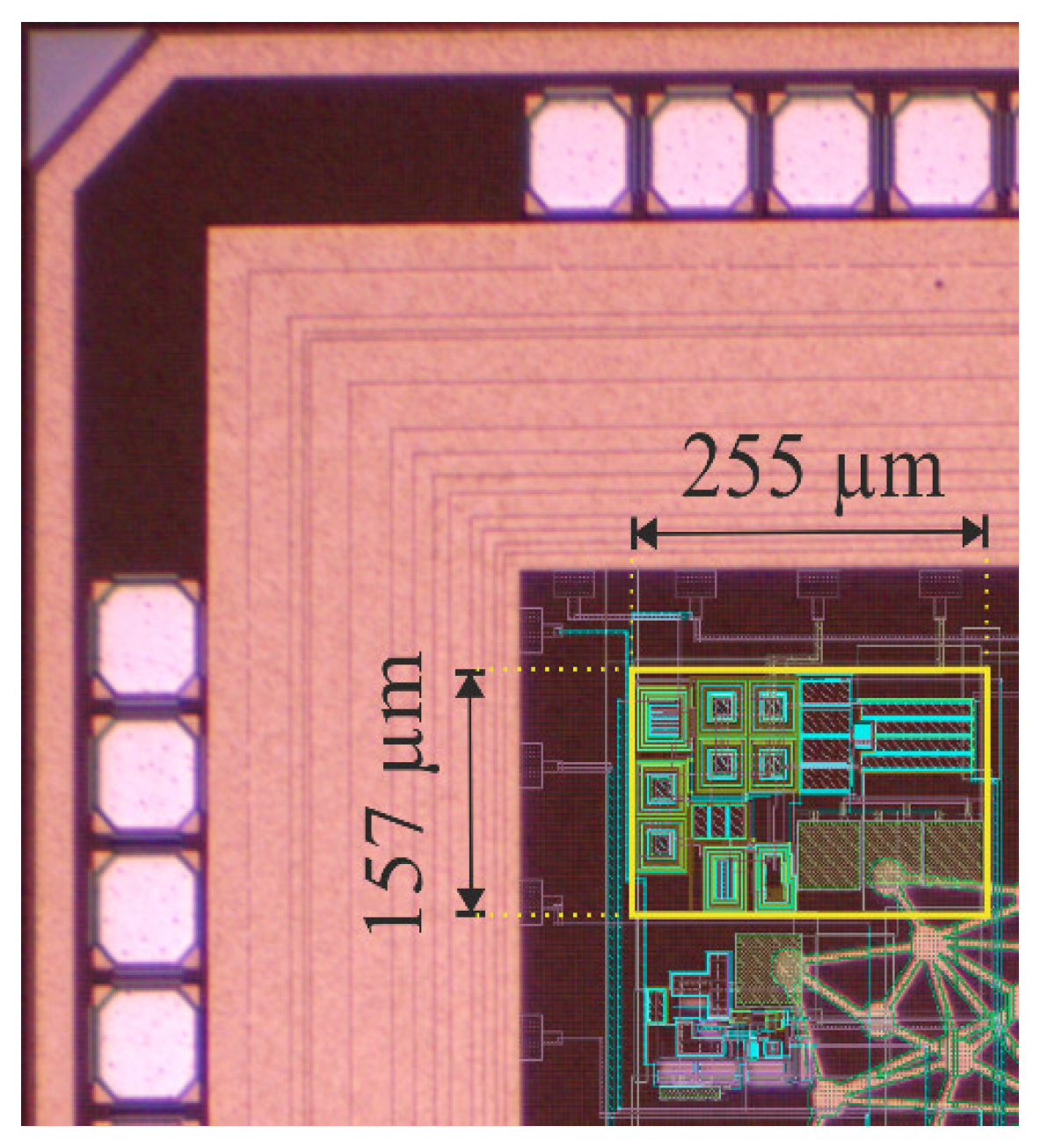
The open-loop amplifier circuit was fabricated in a 0.35 µm CMOS technology by ON Semiconductor Corporation with 3 V supply voltage as an example of a mature and low-cost technology. A microphotograph of the die, featuring highlighted dimensions (255 µm × 157 µm) of the circuit, is presented in Figure 4. The layout is superimposed for clarity. To drive oscilloscope probes for testing, an on-chip buffer is cascaded with the amplifier output. Its power is subtracted from the measured chip power to estimate the power consumed by only the amplifier. With a dual supply voltage of 1.5 V for the output stage (VDD = 3.0 V, VSS = 0 V) and 1.5 V for the input stage (Vsplit = 1.5 V), and a bias current Ibias of 3 µA (30 µA tail current), the total amplifier power estimate agrees well with the result expected from (6).

3.1. Evaluation of the Amplifier Chip

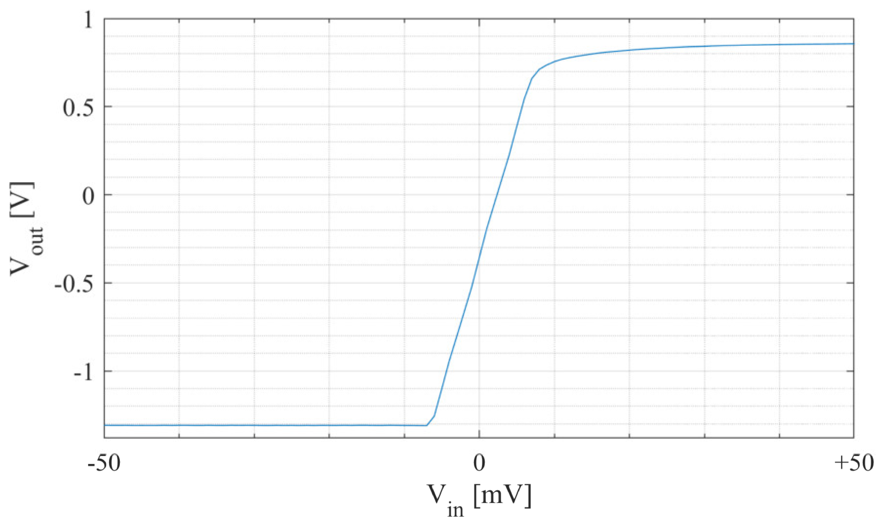
Initially, the CM voltage is set to 2.25 V using an external voltage source. The internal bias network is employed in later measurements as annotated. A differential DC sweep of the inputs was performed, and the output voltage was observed using an oscilloscope. Figure 5 shows a detailed view of the slope around 0 V. By utilizing the full supply voltage at the output stage, a DC output swing of 2.15 V is achieved. The low-frequency gain of the amplifier is determined from the slope of the curve as 105 V/V.
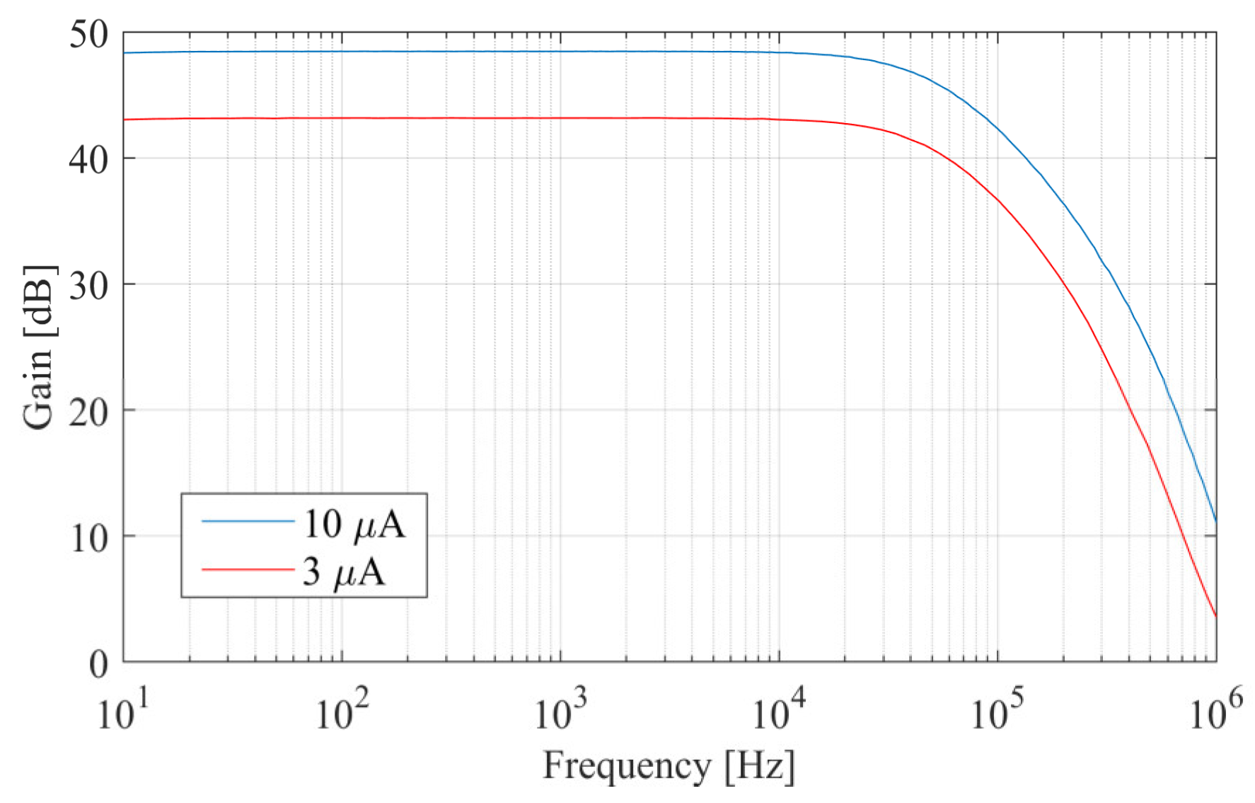
For the measurement of AC gain and phase, a 2 mV differential input signal with the same CM of 2.25 V was applied. The measurement results, captured with a lock-in amplifier, are presented in Figure 6. A differential AC gain of about 104 V/V (40.3 dB) with a bandwidth of approximately 55 kHz is observed. The measured phase is slightly shifted by the test buffer but remains flat within the usable bandwidth. Altering the amplifier bias current changes the gain as expected and shown in Figure 7 for Ibias set to 3 µA and 10 µA, respectively.
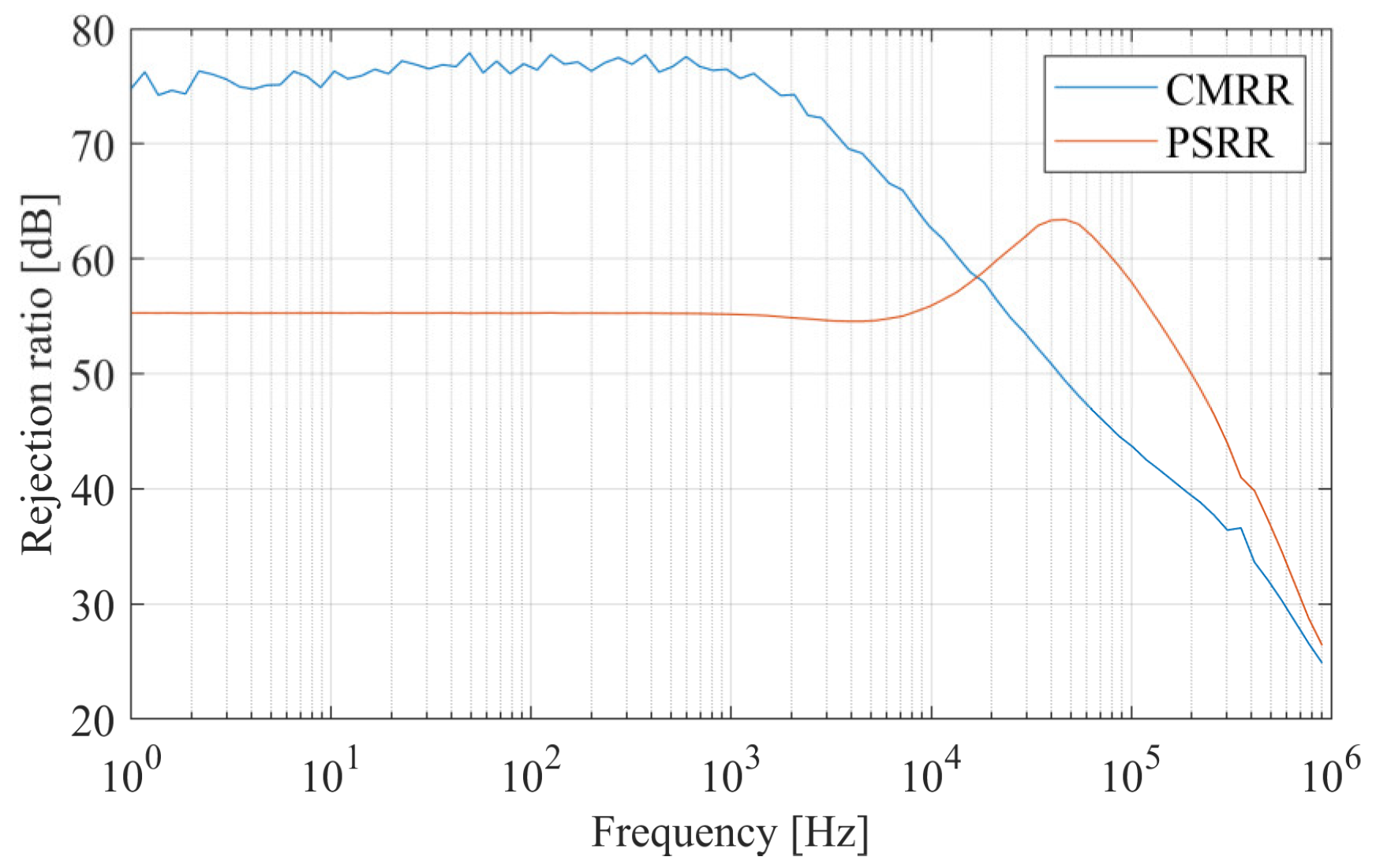
Figure 8 shows the CM rejection ratio (CMRR) and power-supply rejection ratio (PSRR) measured with 50 mV sinusoidal test signals. The CMRR is approximately 75 dB, and the PSRR is 55 dB.
To determine the IRN, the output voltage noise (ORN) was measured with the amplifier inputs both shorted to the CM voltage of 2.25 V. The ORN was then divided by the gain previously measured. The resulting IRN is shown in Figure 9. A noise floor of about 7 nV/√Hz and an integrated noise of 923 nVrms in the relevant frequency band of 100 Hz –10 kHz is obtained. Integration up to 50 kHz, measurable by our equipment, yields 1.86 µVrms. The flicker-noise corner frequency is estimated at 3 Hz. With a total measured current consumption of 67 µA, the NEF is calculated as 2.84, and the PEF is 18.3. Without the split-voltage architecture, the PEF rises to 24.2. Therefore, this setup improves the PEF by 25% and could be further improved if Vsplit is set to its maximum value of 2 V, leading to a PEF of 10.5 (57% improvement).
The amplifier is now biased with the on-chip CM voltage instead of the external CM source. The internal CM level measured at the amplifier inputs is again 2.25 V. An AC test signal is applied via off-chip 10 µF capacitors, and the frequency plot is also shown in Figure 6. An elevated measured IRN floor of approximately 25 nV/√Hz is observed and attributed to the bias network. Over the bandwidth of 100 Hz–10 kHz, an NEF of 3.15 is determined. A PEF of 22.5 is achieved when using the internal resistor network.

3.2. Earthworm Action Potential

The open-loop amplifier is demonstrated in a practical measurement, in which APs of an earthworm (Lumbricus terrestris) are recorded. The general outline of the procedure is described in [21]. After approximately 5 min of exposure to a 10%-ethanol solution, the worm is connected to three electrodes in a 4 cm pitch. Uncoated acupuncture needles with a diameter of 0.25 mm and a length of 40 mm are used as electrodes. The length of the needle allows for secure anchoring on the measuring substrate and attachment of the measurement cables.
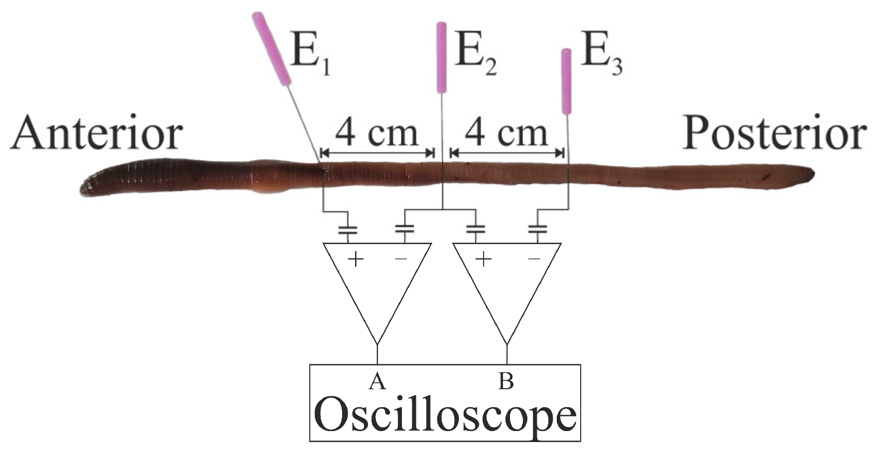
The electrodes are alternately connected to the positive and negative terminals of two amplifiers, as is done, for example, in velocity selective recording (VSR) techniques [22]. Figure 10 shows a schematic diagram of the setup. Since the AP is very small, each amplifier is operated with an increased bias current of 10 µA. Each input is connected through a 10 µF capacitor and using the on-chip resistor network.
In Figure 11a, a measured earthworm AP is shown, which was triggered by touching the head with a wooden stick. Since the amplifiers are distributed along the length of the worm, the units record the AP with a relative time delay. The time interval between the two AP peaks in Figure 11a is 1.3 ms, which corresponds to a propagation velocity of 30.76 m/s. This value falls within the expected range for the medial giant fiber, which transmits information from the anterior to the posterior part of the worm [21]. The measurement of an AP of the lateral giant fiber is shown in Figure 11b. Here, the AP propagates from the tail towards the head, induced by touching the tail. As described in [21], it has a weaker amplitude than an AP of the medial giant fiber and a significantly lower velocity. In this case, a velocity of 6.6 m/s was determined, which falls within the expected range. Moreover, conversely, to the recording in Figure 11a, the AP now appears first on amplifier channel B and later on channel A, indicating the reversed direction of propagation.

4. Comparison

In Table 2, the split-voltage amplifier is compared with other recent low-noise amplifiers. The amplifier presented here exhibits a bandwidth of 50 kHz, which is larger than needed for pure biomedical signals. Reducing the current delivered to the output stage by adjusting the mirror ratio M5:M6 and M3:M4 in Figure 2a would lower the bandwidth and further reduce the power consumption. This, however, would negatively affect the absolute noise performance and was therefore avoided here. The bandwidth is similar to the one presented in [23], as well as a similar noise floor and NEF while requiring only one-third of the power. Both this paper and [23] employ lateral bipolar transistors. The integrated noise of the split-voltage amplifier is lower than that of all the other designs in this comparison. In terms of NEF and PEF [24] and [5] perform better, employing a more complex current-reuse and inverter-stacking approach. However, as regards the absolute IRN, our circuit is better by a factor of almost six compared to [5]. This shows that the design targets differ, and a comparison of these metrics alone is not entirely effective. For example, the output range of [5] is lower than the full range provided by our solution, and a design suitable for the targeted application should be chosen.
The proposed amplifier occupies a very small active area of 0.04 mm2. Normalizing the area to account for the different technology node sizes by dividing the area by the square of the technology size, shows most clearly the size advantage of the proposed approach.
Without the split-voltage approach, i.e., lowering Vsplit to VSS, the PEF would rise to 24.2. Thus, in this setup, the split-voltage approach improved the power efficiency by 25%.

5. Conclusions

The split-voltage amplifier offers a compelling solution for certain low-power, low-noise signal acquisition applications. A practical recording of AP from the medial and lateral giant fibers of an earthworm is presented as an example in which a pair of amplifiers with an internal CM bias circuit was AC-coupled to recording electrodes. The design offers competitive performance with a bandwidth of 55 kHz, a noise floor of 7 nV/√Hz, low flicker noise, an NEF of 2.84, and a PEF of 18.3 with a very small area while at the same time, the full output range is available. This design improves the PEF by 25% compared to a conventional full-voltage supply. The approach can be applied to many conventional amplifiers without major design changes. The practical implementation of a split power supply using standard batteries yields a simple and effective setup, making it a potentially valuable asset in various research and monitoring applications.

Author Contributions

Conceptualization, S.S. and R.R.; methodology, S.S. and R.R.; validation, S.S. and R.R.; formal analysis, S.S. and R.R.; investigation, S.S. and R.R.; resources, R.R.; data curation, S.S.; writing—original draft preparation, S.S. and R.R.; writing—review and editing, S.S. and R.R.; visualization, S.S. and R.R.; supervision, R.R.; project administration, R.R.; funding acquisition, R.R. All authors have read and agreed to the published version of the manuscript.

Funding

This work was partially funded by the Deutsche Forschungsgemeinschaft (DFG, German Research Foundation)—Project-ID 434434223—SFB 1461. We acknowledge financial support by Land Schleswig-Holstein within the funding programme Open Access Publikationsfonds.

Data Availability Statement

The original contributions presented in the study are included in the article, further inquiries can be directed to the corresponding author.

Conflicts of Interest

The authors declare no conflicts of interest. The funders had no role in the design of the study; in the collection, analyses, or interpretation of data; in the writing of the manuscript; or in the decision to publish the results.

References

  1. Rieger, R.; Taylor, J. Design Strategies for Multi-Channel Low-Noise Recording Systems. Analog Integr. Circuits Signal Process. 2009, 58, 123–133. [Google Scholar] [CrossRef]
  2. Leung, L.-F.; Tsui, C.-Y. Energy-Aware Synthesis of Networks-on-Chip Implemented with Voltage Islands. In Proceedings of the 2007 44th ACM/IEEE Design Automation Conference, San Diego, CA, USA, 4–8 June 2007; pp. 128–131. [Google Scholar] [CrossRef]
  3. Russo, P.; Yengui, F.; Pillonnet, G.; Taupin, S.; Abouchi, N. Switching Optimization for Class-G Audio Amplifiers with Two Power Supplies. Circuits Syst. 2012, 3, 90–98. [Google Scholar] [CrossRef]
  4. Johnson, B.; Molnar, A. An orthogonal current-reuse amplifier for multi-channel sensing. IEEE J. Solid-State Circuits 2013, 48, 1487–1496. [Google Scholar] [CrossRef]
  5. Shen, L.; Lu, N.; Sun, N. A 1-V 0.25-μW Inverter Stacking Amplifier with 1.07 Noise Efficiency Factor. IEEE J. Solid-State Circuits 2018, 53, 896–905. [Google Scholar] [CrossRef]
  6. Simmich, S.; Rieger, R. Analysis of Current-Reuse and Split-Voltage Topology for Biomedical Amplifier Arrays. In Proceedings of the 2022 17th Conference on Ph.D Research in Microelectronics and Electronics (PRIME), Villasimius, Italy, 12–15 June 2022. [Google Scholar] [CrossRef]
  7. Kim, C.; Jang, A.; Kim, S.; Cho, S.; Lee, D.; Kim, Y.-J. A Wearable ECG Monitoring System Using Microneedle Electrodes for Small Animals. IEEE Sens. J. 2023, 23, 21873–21881. [Google Scholar] [CrossRef]
  8. Zhang, Y.; Yang, C.; Sun, J.; Li, Z.; Gao, H.; Luo, Y.; Xu, K.; Pan, G.; Zhao, B. A Wireless Headstage System Based on Neural-Recording Chip Featuring 315 nW Kickback-Reduction SAR ADC. IEEE Trans. Biomed. Circuits Syst. 2023, 17, 105–115. [Google Scholar] [CrossRef]
  9. Chang, Y.; Jang, J.; Cho, J.; Lee, J.; Son, Y.; Park, S.; Kim, C. Seamless Capacitive Body Channel Wireless Power Transmission toward Freely Moving Multiple Animals in an Animal Cage. IEEE Trans. Biomed. Circuits Syst. 2022, 16, 714–725. [Google Scholar] [CrossRef]
  10. Jia, Y.; Lee, B.; Kong, F.; Zeng, Z.; Connolly, M.; Mahmoudi, B.; Ghovanloo, M. A Software-Defined Radio Receiver for Wireless Recording from Freely Behaving Animals. IEEE Trans. Biomed. Circuits Syst. 2019, 13, 1645–1654. [Google Scholar] [CrossRef]
  11. Tasneem, N.T.; Biswas, D.K.; Reza, S.; Becker, A.; Mahbub, I. Multichannel Electrophysiological Recording with Spike Detection and Sorting in a Duty-cycled Wireless Optogenetic Headstage. IEEE Sens. J. 2023, 23, 26075–26086. [Google Scholar] [CrossRef]
  12. Kanchwala, M.A.; McCallum, G.A.; Durand, D.M. A Miniature Wireless Neural Recording System for Chronic Implantation in Freely Moving Animals. In Proceedings of the 2018 IEEE Biomedical Circuits and Systems Conference (BioCAS), Cleveland, OH, USA, 17–19 October 2018; pp. 1–4. [Google Scholar] [CrossRef]
  13. Sun, J.; Yang, C.; Zhang, Y.; Li, Z.; Gao, H.; Yu, C.; Yu, C.; Luo, Y.; Xu, K.; Pan, G.; et al. Live Demonstration: A BLE Wireless Neural-Recording Headstage on Freely-Moving Rat. In Proceedings of the 2022 IEEE Biomedical Circuits and Systems Conference (BioCAS), Taipei, Taiwan, 13–15 October 2022; p. 244. [Google Scholar] [CrossRef]
  14. Guo, Y.; Ma, Z.; Sheng, D.; Lei, J.; Zhang, M.; Wang, T.; Sheng, X. A Wireless Neural Interface Device for Simultaneous Optogenetics and Neural Recording. In Proceedings of the 2023 IEEE Biomedical Circuits and Systems Conference (BioCAS), Toronto, ON, Canada, 19–21 October 2023; pp. 1–5. [Google Scholar] [CrossRef]
  15. Szuts, T.; Fadeyev, V.; Kachiguine, S.; Sher, A.; Grivich, M.V.; Agrochão, M.; Hottowy, P.; Dabrowski, W.; Lubenov, E.V.; Siapas, A.G.; et al. A wireless multi-channel neural amplifier for freely moving animals. Nat. Neurosci. 2011, 14, 263–269. [Google Scholar] [CrossRef]
  16. Papadopoulou, A.; Hermiz, J.; Grace, C.; Denes, P. A Modular 512-Channel Neural Signal Acquisition ASIC for High-Density 4096 Channel Electrophysiology. Sensors 2024, 24, 3986. [Google Scholar] [CrossRef] [PubMed]
  17. Simmich, S.; Bahr, A.; Rieger, R. Noise Efficient Integrated Amplifier Designs for Biomedical Applications. Electronics 2021, 10, 1522. [Google Scholar] [CrossRef]
  18. Rieger, R.; Taylor, J.; Demosthenous, A.; Donaldson, N.; Langlois, P.J. Design of a low-noise preamplifier for nerve cuff electrode recording. IEEE J. Solid-State Circuits 2003, 38, 1373–1379. [Google Scholar] [CrossRef]
  19. Steyaert, M.S.J.; Sansen, W.M.C. A micropower low-noise monolithic instrumentation amplifier for medical purposes. IEEE J. Solid-State Circuits 1987, 22, 1163–1168. [Google Scholar] [CrossRef]
  20. Muller, R.; Gambini, S.; Rabaey, J.M. A 0.013 mm2, 5 μW, DC-Coupled Neural Signal Acquisition IC with 0.5 V Supply. IEEE J. Solid-State Circuits 2012, 47, 232–243. [Google Scholar] [CrossRef]
  21. Shannon, K.M.; Gage, G.J.; Jankovic, A.; Wilson, W.J.; Marzullo, T.C. Portable conduction velocity experiments using earthworms for the college and high school neuroscience teaching laboratory. Adv. Physiol. Educ. 2014, 38, 62–70. [Google Scholar] [CrossRef]
  22. Rieger, R.; Taylor, J. A Switched-Capacitor Front-End for Velocity-Selective ENG Recording. IEEE Trans. Biomed. Circuits Syst. 2013, 7, 480–488. [Google Scholar] [CrossRef]
  23. Kim, H.; Kwon, Y.; You, D.; Choi, H.W.; Kim, S.H.; Heo, H.; Kim, C.-Y.; Lee, H.-D.; Ko, H. Low-Noise Chopper Amplifier Using Lateral PNP Input Stage with Automatic Base Current Cancellation. IEEE Trans. Circuits Syst. II Exp. Briefs 2021, 68, 2297–2301. [Google Scholar] [CrossRef]
  24. Zhang, J.; Zhang, H.; Sun, Q.; Zhang, R. A Low-Noise, Low-Power Amplifier with Current-Reused OTA for ECG Recordings. IEEE Trans. Biomed. Circuits Syst. 2018, 12, 700–708. [Google Scholar] [CrossRef]
  25. Liu, J.; Allstot, D.J. A Chopper-Stabilized Switched-Capacitor Front-End for Peripheral Nervous System Recording. IEEE Trans. Circuits Syst. I Reg. Papers 2023, 70, 3065–3074. [Google Scholar] [CrossRef]
  26. Zhou, Z.; Zhu, L.; Yang, R.; Li, J.; Wang, W.; Pan, J.; Liu, M.; Wang, K.; Wang, Z. A High CMRR Instrumentation Amplifier Employing Pseudo-Differential Inverter for Neural Signal Sensing. IEEE Sens. J. 2022, 1, 419–427. [Google Scholar] [CrossRef]
  27. Livanelioglu, C.; Choi, W.; Kim, D.; Liao, J.; Incandela, R.; Jang, T. A Compact and PVT-Robust Segmented Duty-Cycled Resistor Realizing TΩ Impedances for Neural Recording Interface Circuits. IEEE Solid-State Circuits Lett. 2023, 6, 25–28. [Google Scholar] [CrossRef]
  28. Lee, B.; Ghovanloo, M. An Adaptive Averaging Low Noise Front-End for Central and Peripheral Nerve Recording. IEEE Trans. Circuits Syst. II Exp. Briefs 2018, 65, 839–843. [Google Scholar] [CrossRef]
  29. Rezaei, M.; Maghsoudloo, E.; Bories, C.; De Koninck, Y.; Gosselin, B. A Low-Power Current-Reuse Analog Front-End for High-Density Neural Recording Implants. IEEE Trans. Biomed. Circuits Syst. 2018, 12, 271–280. [Google Scholar] [CrossRef] [PubMed]
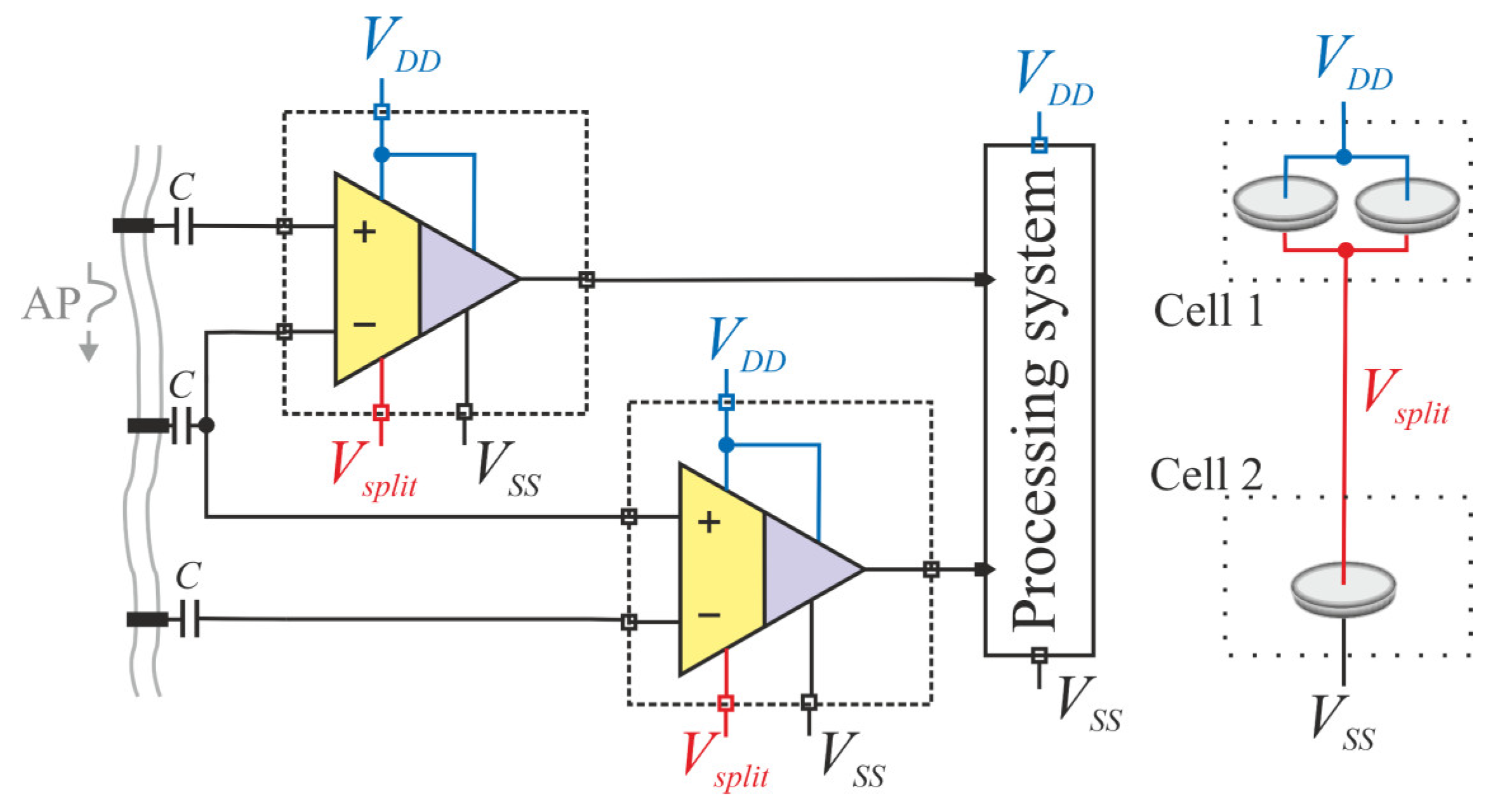
Figure 1. System example for the recording of action potentials with a pair of split-voltage amplifiers. Voltage is supplied by two coin cells cell 1 and cell 2, where the capacity of cell 1 may be made larger than that of cell 2.
Jlpea 14 00045 g001
Figure 2. (a) Schematic diagram of the split-voltage amplifier and (b) the optional on-chip bias network. The positive supply voltage VDD is identical for all blocks, the lower supply voltages differ as shown.
Jlpea 14 00045 g002
Figure 3. Simulated influence of the bias current on the amplifier performance.
Jlpea 14 00045 g003
Figure 4. Microphotograph of a corner of the die with the drawn layout of the amplifier in the yellow box. The dimensions of the amplifier are 157 µm × 255 µm.
Jlpea 14 00045 g004
Figure 5. Measured differential DC-Sweep of the input stage with a common-mode bias Vcm of 2.25 V.
Jlpea 14 00045 g005
Figure 6. Measured gain and phase, alternatively with external and internal common-mode sources.
Jlpea 14 00045 g006
Figure 7. Gain measured for different bias currents Ibias of 3 µA and 10 µA. The midband gain changes by 8 dB.
Jlpea 14 00045 g007
Figure 8. Measured CMRR and PSRR with external common-mode source.
Jlpea 14 00045 g008
Figure 9. Measured input-referred voltage noise with external CM source.
Jlpea 14 00045 g009
Figure 10. Setup for the two-channel action potential recording of the medial and lateral giant fiber with two split-voltage amplifiers in overlapping dipole configuration.
Jlpea 14 00045 g010
Figure 11. (a) Recorded action potential of the median giant fiber with a velocity of 30.76 m/s. (b) Recorded action potential of the lateral giant fiber with a velocity of 6.6 m/s.
Jlpea 14 00045 g011
Table 1. Component dimensions for Figure 2a.
DeviceW/L in µm/µmVoltages Used in (1), (2), (3)
Q1, Q210/10VBE = 0.7 V
Q320/20-
M120/1-
M2200/1VDS_Mbias2 = 0.038 V
M3, M570/8VGS_M3,5 = 0.876 V
M4, M680/8-
M7, M850/0.4-
M9, M1070/15-
Ibias3 µA
Table 2. Comparison of this work to other recently published amplifiers on a per-channel basis.
This WorkTCAS-I
’23 [25]
TBioCAS ’18 [24]TCAS-II ’21 [23]Sensors J. ’22 [26]SSC-L’23
[27]
TCAS-II ’18 [28]JSSC’18
[5]
TBioCAS
’18 [29]
Technology [nm]350180350180180180180180180
Input transistorLat. BJTCMOSCMOSLat. BJTCMOSCMOSCMOSCMOSCMOS
Supply voltage [V]31.823.31.81.8111.8
Bandwidth [Hz]1–55 k170–96800.2–2000.1–39.2 k200–5 k0.2–5 k20–15 k250–10 k1–10 k
IRN [µVrms]0.923
(0.1–10 kHz)
2.21
(1–100 kHz)
2.05
(0.1–10 kHz)
-3.6
(0.2–5 kHz)
6.61
(0.2–5 kHz)
1.8
(10–17 kHz)
5.5
(0.25–10 kHz)
3.2
(1–10 kHz)
Noisefloor [nV/√Hz]716-5.534870105060
NEF2.843.52.263.224.353.51.071.94
PEF18.32210.234.233.34512.51.156.77
Power [µW]15228.980.320481.88.30.974.40.254.5
Area [mm2]0.040.1360.180.2970.0260.0390.280.020.072
Normalized Area326.8 k4.2 M1.46 M9.2 M802 k1.2 M8.6 M617.3 k2.22 M
1/f corner [Hz]3-~ 1 k5~1 k~2 k~8300200
Disclaimer/Publisher’s Note: The statements, opinions and data contained in all publications are solely those of the individual author(s) and contributor(s) and not of MDPI and/or the editor(s). MDPI and/or the editor(s) disclaim responsibility for any injury to people or property resulting from any ideas, methods, instructions or products referred to in the content.