Article

0.7 V Supply SC Circuits with Relaxed Slew Rate Requirements Using GB-Enhanced Multiple-Output Class AB/AB Op-Amps

by
Hector Daniel Rico-Aniles
1,
Anindita Paul
2,
Jaime Ramirez-Angulo
3,*,
Antonio Lopez-Martin
4 and
Ramon G. Carvajal
5
1
Department of Engineering, North Central College, Naperville, IL 60540, USA
2
Department of Engineering Sciences, Morehead State University, Morehead, KY 40351, USA
3
Klipsch School of Electrical and Computer Engineering, New Mexico State University, Las Cruces, NM 88003, USA
4
Department of Electrical and Electronic Engineering, Public University of Navarra, 31006 Pamplona, Spain
5
Departamento de Ingenieria Electronica, Escuela Superior de Ingenieros Universidad de Sevilla, E41092 Sevilla, Spain
*
Author to whom correspondence should be addressed.
J. Low Power Electron. Appl. 2025, 15(2), 24; https://doi.org/10.3390/jlpea15020024
Submission received: 7 February 2025 / Revised: 11 April 2025 / Accepted: 11 April 2025 / Published: 15 April 2025

Abstract

:
A family of improved low-voltage switched-capacitor circuits is introduced. It is based on the utilization of multiple-output class AB/AB op-amp architectures that provide true sample and hold outputs that are not subject to a reset phase as with conventional switched-capacitor circuits. This feature essentially relaxes the op-amp slew rate requirements, allowing a higher speed and simple low-voltage operation. A power-efficient GB boosting technique based on resistive local common mode feedback is used to significantly improve the GB and internal/external slew rate of the op-amps with only a 36.5% additional power dissipation.

1. Introduction

Switched-capacitor (SC) circuits were developed to overcome the accuracy limitations of integrated RC active continuous-time circuits. They allow the implementation of integrated filters with accurate time constants/frequency responses that do not require complex tuning circuitry and that are based on capacitor ratios and a highly accurate external reference clock frequency fclk. For this reason, they have been for many years essential buildings blocks in many signal-processing integrated systems. Besides traditional applications, SC circuits also offer advantages in many emerging fields that require an ultra-low power dissipation, like body area networks (BANs) in biomedical applications, sensor networks, the internet of things, RF power amplifiers, inductor-free switching-mode converters, etc. [1,2,3,4,5].
Figure 1 and Figure 2 show the implementation of a conventional offset-compensated SC amplifier and a conventional SC first-order low-pass filter, respectively [6,7]. In practice, one of the main problems that limits the speed of SC circuits is the high slew rate (SR) requirements on the op-amps, since the outputs of the op-amps reset to zero (or to another constant value) during one clock phase and excursions from zero to the new sampled value during the other phase. This leads eventually to two large output voltage variations every clock cycle.
This problem can be avoided by using an op-amp with an auxiliary output that provides a true sample and hold signal without a reset to zero, as explained in the following section.
A second important concern for SC circuits and continuous-time analog circuits is the low-voltage operation required in modern deep sub-micrometer CMOS technologies whose nominal working supply voltages have been reduced faster than the threshold voltages with the downscaling of technology. In some cases, the nominal supply voltage in deep sub-micrometer CMOS technology does not even provide enough headroom for conventional analog circuits to be functional, unless MOS transistors operate in the subthreshold. Even in the cases where the nominal supply is sufficient to operate a circuit, lowering the supply voltage of an integrated circuit is highly desirable in order to reduce its power consumption for applications such as wireless and biomedical ones, IoT and RF IDs and especially to significantly reduce the power dissipation of the digital section of the circuit, which usually makes over 90% of the silicon area of a mixed-mode circuit and whose power dissipation is proportional to VDD2. Moreover, low-voltage operation enables a design’s portability across different technologies. Some SC implementation-denoted comparator-based SC circuits have been reported where op-amps are replaced by CMOS inverters and current sources [8,9,10]. This is done in order to reduce power dissipation, improve the slew rate and reduce supply requirements. Additionally, a number of op-amp architectures with an enhanced slew rate have been also reported to satisfy the high slew rate requirements of conventional SC circuits, with sample and reset to zero output signals [11,12,13,14,15,16].
In [17,18,19], schemes for the low-voltage operation of SC circuits were reported. The scheme reported in [17] consists simply of DC shifting the input gates of the op-amp from the conventional mid-supply voltage to a value VSSP or VDDP that is close to the lower or upper supply rails, VSS or VDD, for op-amps with a PMOS or NMOS input differential pair, respectively. This simple low-voltage technique (LVT) can be easily implemented, as illustrated in Figure 1b where an op-amp with an NMOS input differential pair is assumed. Here, low supply operation is possible, since both terminals of the op-amp operate at a reference voltage VDDP that is close to VDD. But this value is canceled out, along with the offset Vos in the signal path, since it is treated as an additional offset term. Unfortunately, this simple low-voltage implementation scheme worsens the SR limitation of the op-amp in SC circuits, since the output reset value is now close to one of the rails instead of to the mid-supply voltage, and the worst-case swing is increased by close to a factor of two. This is depicted in Figure 3 for the case of the SC amplifier of Figure 1 with a nominal gain G = 4 V/V that operates with ±0.35 V supplies in 180 nm CMOS technology that has nominal supplies of ±0.9 V. When the positive input terminal of the op-amp is connected to a voltage VDDP = 0.27 V, the output resets also to VDDP + Vos during phase ϕ, and for the peak negative portion of the signal the required SR is almost doubled, since now a swing close to the supply is required during the reset phase ϕ. The multiple-output op-amp technique addressed above can be used to essentially alleviate this problem in low-voltage SC circuits based on the technique proposed here.
In this paper, the implementation of low-voltage SC filters and amplifiers is presented as example of the proposed technique, but it can be extended to other SC circuits. The schemes are based on the use of op-amps with an auxiliary output that have true sample and hold output signals that greatly alleviate the op-amp slew rate requirements. We also introduce here a power-efficient class AB/AB op-amp that uses a simple GB enhancement technique to essentially improve the slew rate, GB and DC open-loop gain of the op-amp. This allows a higher frequency of operation and improved THD. SC architectures that perform correlated double sampling to cancel out offset can be easily implemented using this technique with a reduced supply voltage and with a very small additional power dissipation and silicon area.
The paper is organized as follows: Section 2 describes the proposed scheme and the GB-enhanced dual-output AB/AB op-amp used. Section 3 discusses simulation results of a low-voltage SC amplifier and a first-order low-pass filter in 180 nm CMOS technology operating with ±0.35 V supply voltages, which correspond to only 40% of the nominal supply voltage (±0.9 V) of this technology. Some conclusions are given in Section 4.

2. Circuit Description

2.1. GB-Enhanced AB/AB Op-Amp with Dual Ouputs

The multiple-output op-amp used to implement the low-voltage SC filter and amplifier is a GB-enhanced AB/AB Miller compensated op-amp with two outputs: the main signal output and an auxiliary low-power output.
Figure 4 shows a single-ended differential amplifier used commonly as the input stage of Miller op-amps. It has a gain AinpAi/2, where Ai = gmro is the intrinsic gain of the MOS transistor, gm is the transconductance gain of the differential pair transistors, and ro is the output resistance of transistors MDP′ and MP1′ (assumed equal for simplicity). The proposed multiple-output op-amp uses a composite input stage that is GB- and slew rate-enhanced, and it is shown in Figure 5. This composite input is formed by two stages. The first stage has a differential pair and uses resistive local common-mode feedback (RLCMFB), provided by resistors RLCMFB [20]. It operates in class AB, has a gain Ainl ≈ 5(Ai/2), and it has enhanced transconductance gmeff ≈ 5 gmP2 as explained in the following subsection.
The two output stages (main and auxiliary) are shown in Figure 6. Output stage 1 shown in Figure 6a is a free class AB amplifier [21] used as the main (signal path) output of the op-amp. In this stage, free class AB dynamic operation is achieved by means of capacitor Cbat and resistor RLarge. The auxiliary output stage 2 shown in Figure 6b is a class A amplifier, and it is used as the low-power auxiliary output of the op-amp. It operates with a bias current 10 times lower than the main output stage.

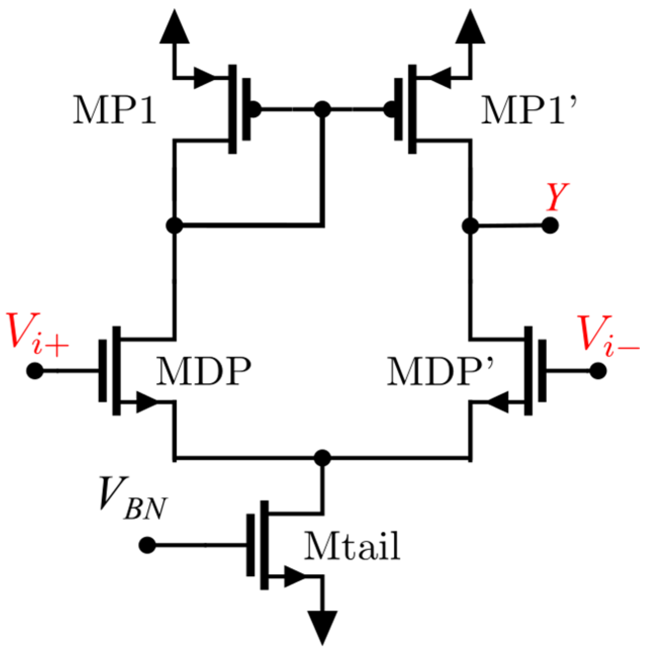
2.2. Operation of the Composite Input State

As indicated above, the composite input stage is formed by a differential amplifier (DA) with resistive local common-mode feedback (MDP, MDP′, MP1, MP1′ and RLCMFB) and a current differencing shell with two branches formed by MN2, MP2, MN2′ and MP2′. This provides the op-amp with an enhanced gain and GB and class AB operation in the input stage. The composite input stage has a voltage gain AI = VoI/Vd given by (1), where gmeffI = ADAgmP2 is the effective transconductance gain of the input stage, RoutI is the output impedance of the composite input stage at node VoI given by (2), and ADA ≈ 5 is the gain enhancement factor of the differential amplifier given by (3). Therefore, the gain of the input stage can be expressed by (4), and it is approximately given by (5).
A I = g m e f f I · R o u t I = A D A g m P 2 · R o u t
R o u t I = r o N 2 | | r o P 2
A D A = V X V X / V i + V i g m D P · R L C M F B
A I = g m D P R L C M F B g m P 2 r o N 2 | | r o P 2
A I = g m D P R L C M F B g m P 2 r o 2 A D A g m P 2 r o 2
As indicated above, the gain of the composite input stage (and of the op-amp) is enhanced by a factor RLCMFBgmP2ADP with reference to the gain of the conventional op-amp using the input stage of Figure 4.
The value of RLCMFB determines the gain and GB enhancement factor. It also determines the high-frequency poles fpX,X at nodes X, X′. These poles are given by (6), where CX,X’ are the parasitic capacitance at nodes X, X′. In order to avoid the phase margin degradation of the open-loop response, they are required to satisfy the condition fpX,X >> GB. The maximum value of the GB enhancement factor (and consequently of RLCMFB) is limited by this condition. In the herein proposed op-amps, RLCMFB had a value of 50 kΩ, which provided a significant GB enhancement factor of approximately 5 and resulted in poles fpX,X with values of fpX,X ≈ 65 MHz, while the op-amp was designed for GB = 25 MHz. This corresponds to fpXX ~ 2.6 GB. Deep sub-micrometer CMOS technologies with finer feature sizes, have a very small capacitances C X , X and make it possible to design op-amps with a higher GB enhancement factor.
f p X , X 1 2 π R L C M F B C X , X
Another advantage of the input stage of Figure 5 is that it operates in class AB. As explained in [20], it generates output currents at node VoI that can be much higher (by close to an order of magnitude) than the bias current Ibias. This prevents the slew rate of the op-amp from being limited by the slew rate of the internal node VoI.
The GB of the op-amp is derived in Equations (7)–(9), where AII = gmMPo(roMPO||roMNo) ≈ gmro/2 is the gain of the output stage(s). From (9), the GB of the op-amp is enhanced by the factor ADP ≈ 5 with respect to the GB of a conventional Miller op-amp with just a moderate increase (~33.3%) in power dissipation due to the composite input stage.
G B = A I A I I f D o m P o l e = g m e f f I R o u t I A I I 2 π A I I R o u t I C C
G B = g m e f f I 2 π C C
G B = A D A g m P 2 2 π C C

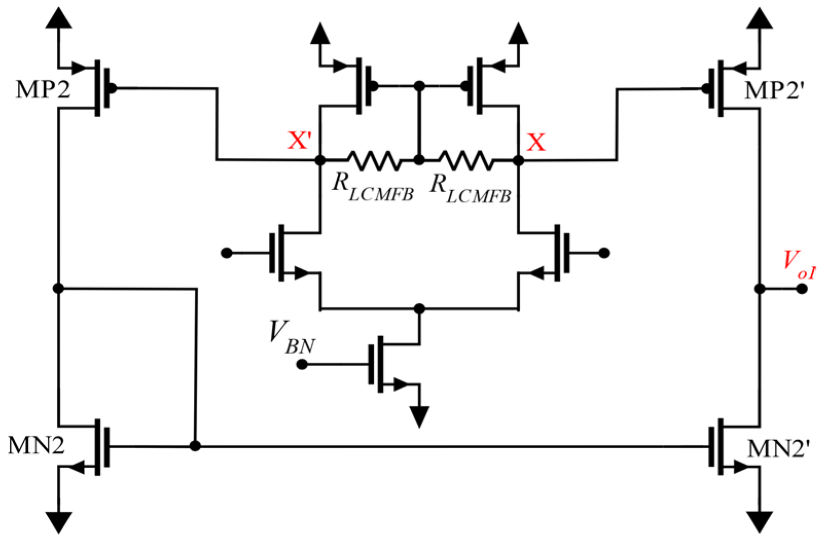
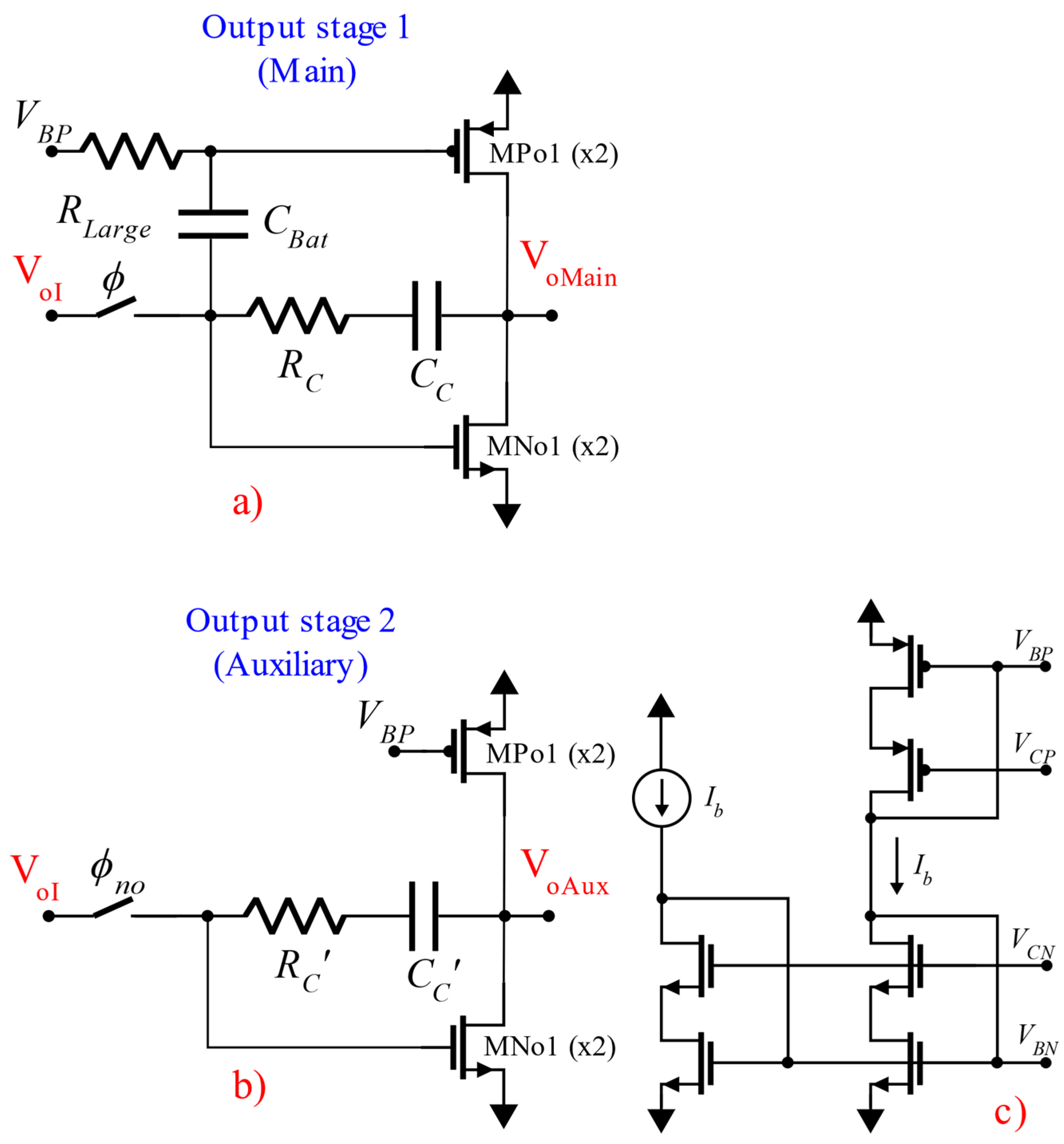
2.3. Operation of Output Stages

As indicated above, the dual-output op-amp used to implement the SC filter and amplifier uses two output stages, denoted the main and auxiliary output stages, which are shown in Figure 6. Output stage 1, shown in Figure 6a, is a free class AB amplifier that is used as the main signal output of the op-amp. Power-efficient free class AB operation at the output node is achieved by means of capacitor Cbat and resistor RLarge [21]. It is denoted as free class AB since it does not require additional power consumption or an increased supply voltage. The output stage 2 shown in Figure 6b is a class A amplifier, and it is used as the auxiliary output of the op-amp. The main output of the op-amp drives the load CL = 15 pF, while the auxiliary output works around the overall offset voltage (Vos + VDDP), drives only the capacitor Cin and does not require a high slew rate, since it is not subject to large voltage variations, given that it remains at an approximately constant voltage throughout the operation of the circuit, as explained below. Figure 6c shows the biasing circuit used to generate VBN and VBP. PMOS and NMOS diode-connected transistors with dimensions W/6L biased with a current Ib are used to generate cascode voltages VCN and VCP. These diode-connected transistors generate voltages VGS′ = VTH + VDSsat′ that have drain–source saturation voltages VDSsat′ ≈ 2.5 VDssat approximately 2.5 times larger than the drain–source saturation voltages of transistors in the main circuit.
The composite input stage sequentially drives the two output stages during each of the clock non-overlapping phases ϕ and ϕno. These blocks leverage the compensation capacitances CC and CC′ to hold the output voltages of each output for close to a whole clock period while they are not in the feedback loop and are disconnected from the input stage. None of the outputs is subject to large changes due to a reset phase, as is the case in conventional SC circuits, and for this reason, the slew rate requirements imposed on the op-amp are greatly relaxed. The auxiliary output stage holds the DC voltage VoAux = VDDP + Vos (see Section 2.4) and can operate with a fraction of the bias current Ibias of the main output stage, since the only load it drives is the sampling capacitor Cin, and it is not subject to large voltage variations.

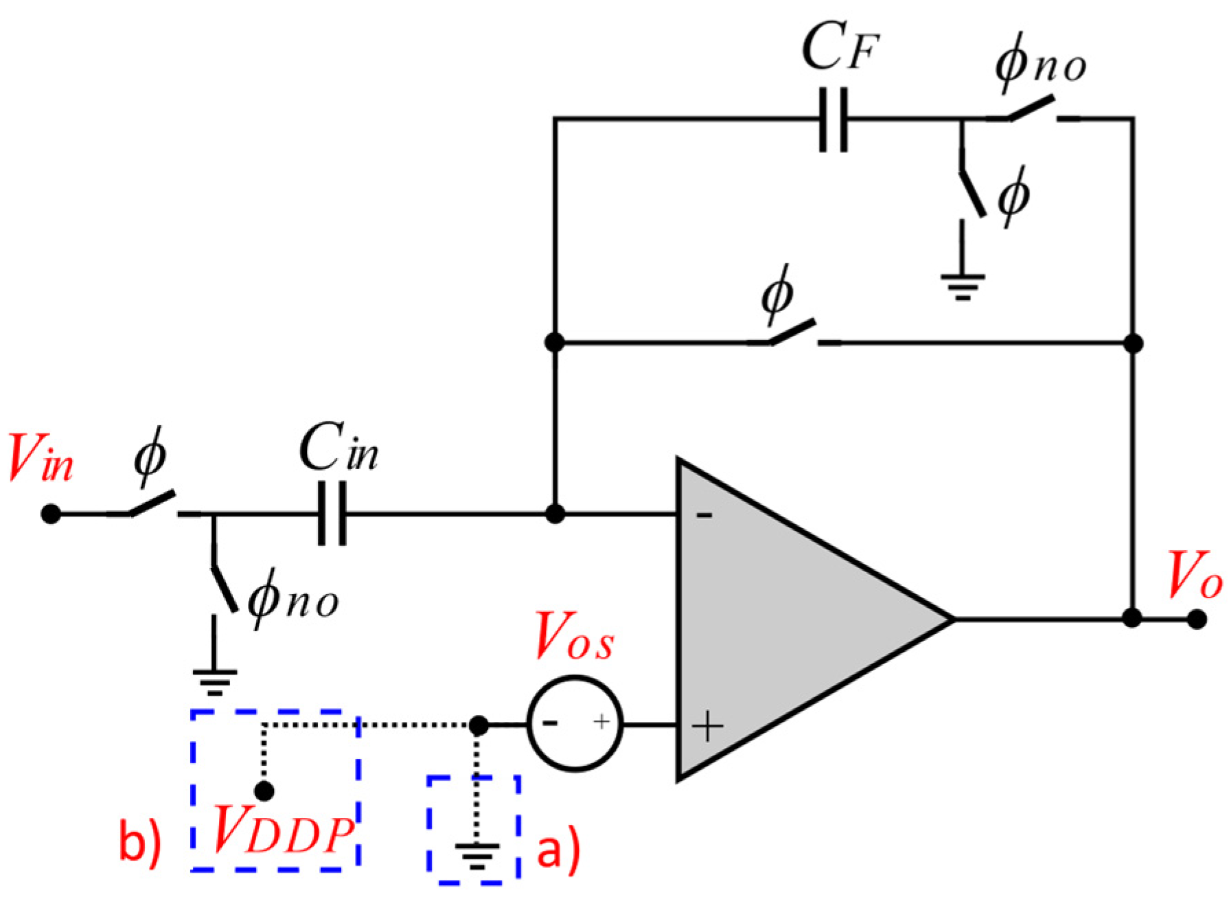
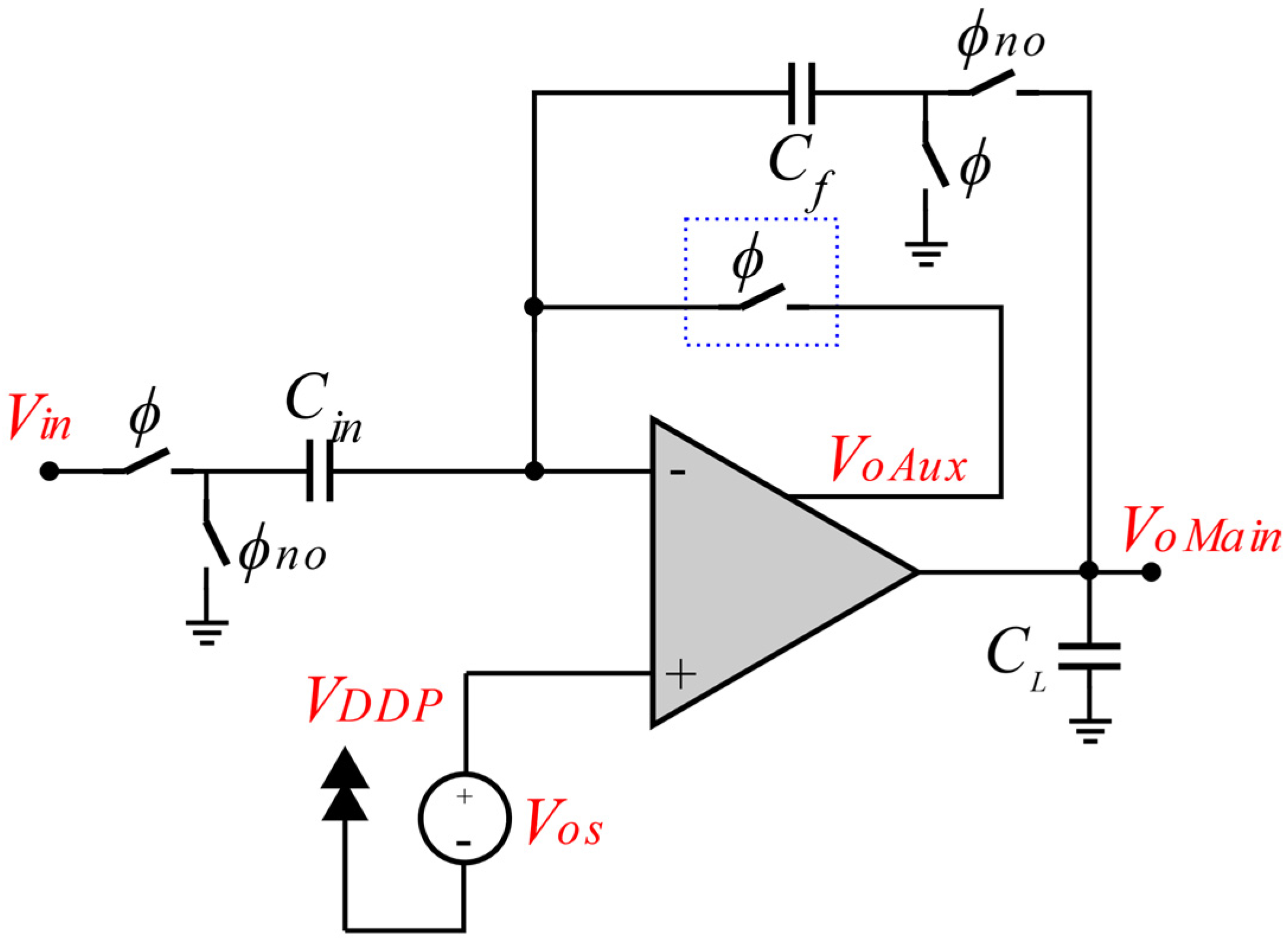
2.4. Low-Voltage SC Amplifier

Figure 7 shows the proposed low-voltage implementation of an SC amplifier with offset compensation using the multiple-output op-amp described in the previous section. The gain A in this circuit is determined by capacitors Cf and Cin, as stated in Equation (10). During phase ϕ, the input of the auxiliary amplifier is connected internally to the output terminal of the input stage, and its output (the auxiliary output) is connected externally to the negative input terminal of the op-amp. In this case, the circuit is configured as a voltage follower with respect to VoAux. This forces the auxiliary output to settle to a voltage VoAux = VDDP + Vos. At the same time, Cin and Cf charge to voltages VCin = Vin − (Vos + VDDP) and VCF = Vos + VDDP, respectively. During the following phase ϕno, the auxiliary output is disconnected from VoI, and the main output is connected internally to VoI and externally to Cf The charge stored in Cin is transferred to Cf, so that the main output voltage settles to the amplified version of the sampled input signal, VoMain = (Cin/Cf)Vin. This voltage is held at the main output by the compensation capacitor CC during the entire clock cycle, even after the main output is disconnected from the input stage during phase ϕ. Therefore, the main output is not reset to zero as in conventional SC circuits. It just changes to the new sampled value every clock cycle at the beginning of phase ϕno. On the other hand, the auxiliary output remains at the constant voltage VoAux = Vos + VDDP throughout the operation of the circuit, and for this reason it is not subject to voltage changes and does not require a high slew rate.
A = V o V i = C i n C f

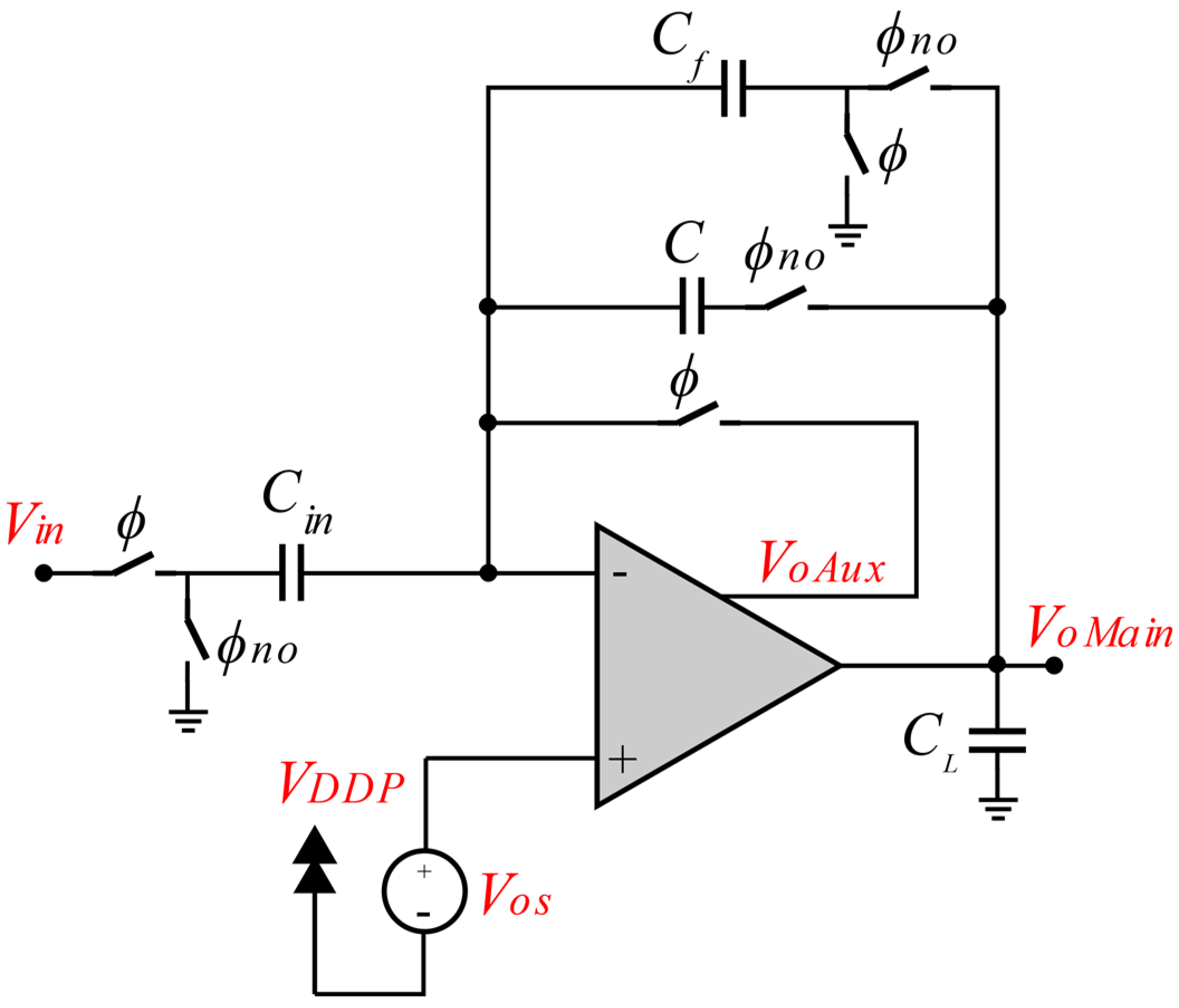
2.5. Low-Voltage SC Low-Pass Filter

The proposed low−voltage implementation of an SC low−pass filter using a two-output op-amp is shown in Figure 8. This implementation also performs a correlated double sampling that leads to offset compensation. The value VDDP connected at the positive input terminal of the op-amp is treated as an additional offset term that is also stored and compensated for in the auxiliary output during phase ϕno. A value VDDP = VDDVSDsat is used to allow the PMOS transistor MPo1 of the auxiliary output stage to remain in saturation. This allows the low-voltage operation of the circuit, since the capacitors act as floating DC sources that maintain the inputs of the op-amp to a voltage VDDP + Vos close to the positive rail, providing enough headroom for the NMOS input differential pair to operate with a low supply voltage. In this scheme, the capacitors Cf and Cin behave as resistors with equivalent values Rf = 1/fclkCf and Rin = 1/fclkCin, where fclk = 1/Tclk is the clock frequency. Therefore, the cutoff frequency of the circuit is determined by the combination of the feedback capacitors Cf and C and is given by (11).
f c u t o f f = f c l k C f 2 π C

3. Simulation Results

The proposed low-voltage SC amplifier and low-pass filter circuits of Figure 7 and Figure 8 were simulated using Cadence Design Framework II for commercial 180 nm CMOS technology. This technology has a nominal supply voltage Vsupply = 1.8 V and exhibits NMOS and PMOS threshold voltages of VthN ≈ |VthP| ≈ 0.55 V. The circuit was designed to operate with dual supplies VDD = −VSS = 0.35 V (40% of the nominal supply) and a bias current Ibias = 10 µA, leading to a 43.4 µW quiescent power consumption. Both output stages (main and auxiliary) use Miller compensation capacitors and resistors CC = 2 pF, RC = 32 kΩ. The main output stage drives a 20 pF load capacitance. A comparison of the op-amp performance with some previously reported proposals is shown in Table 1. The two-stage op-amp used to implement the proposed SC amplifier has a gain–bandwidth product GB = 23 MHz, a phase margin PM = 45° and a slew rate SR = 9.41 V/µs. Therefore, the proposed amplifier exhibits a small signal figure of merit FOMSS = 10,698 (MHz*pF/mW) and a large signal figure of merit FOMLS = 4376 ((V/µs)*(pF/mW)). In practice, the high speed of a circuit is determined by both the FOMSS and FOMLS. A global high-speed figure of merit is determined by the geometric mean of the FOMSS and FOMLs. The FOMGlobal is 6842 for the proposed GB-enhanced class AB op-amps. All the figures of merit are described by Equations (12)–(14). From Table 1, it can be asserted that the proposed circuit has the highest FOMSS and highest FOMGlobal.
Regarding the large signal figure of merit (FOMLS), the proposed circuit exhibits a higher value than the state-of-the-art work presented in Table 1, except for reference [22]. The FOMLS is important for circuits with high slew rate requirements. The proposed low-voltage switched-capacitor circuits were designed with dual-output op-amps that have true sample and hold outputs. The op-amp does not need to react fast to a long step change, which essentially relaxes the high slew rate requirements. On the contrary, in the case of the conventional sample and hold circuit with a conventional op-amp, the outputs of the op-amps reset to zero (or to another constant value) during one clock phase and excursion from zero to the new sampled value during the other phase. This leads to two significant output voltage variations every clock cycle. Thus, the conventional op-amp needs to have a high slew rate.
F O M S S = G B C L P D i s s M H z p F m W
F O M L S = S R C L P D i s s ( V / μ s ) p F m W
F O M G l o b a l = F O M L S F O M S S  

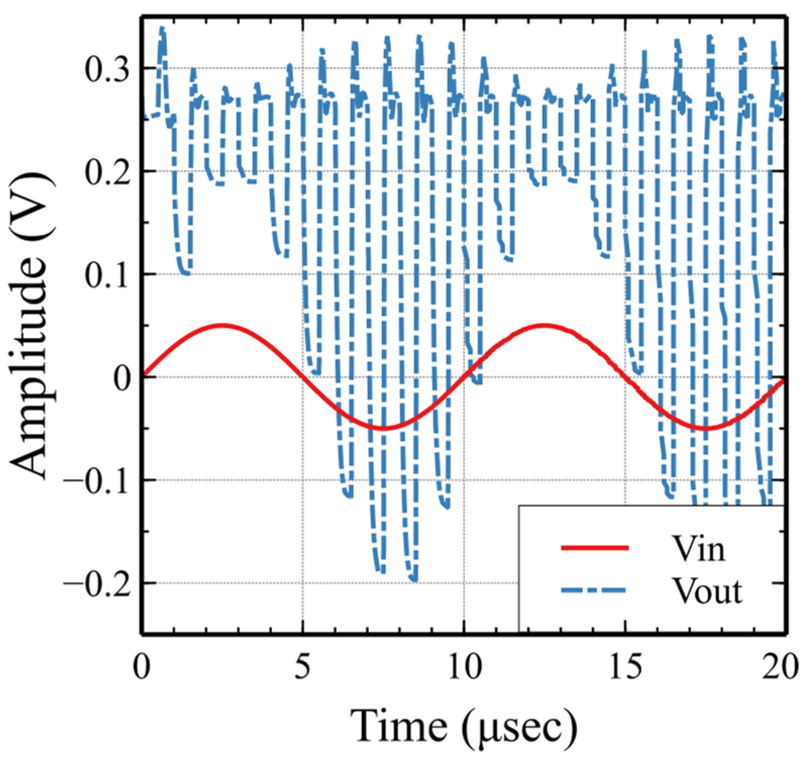
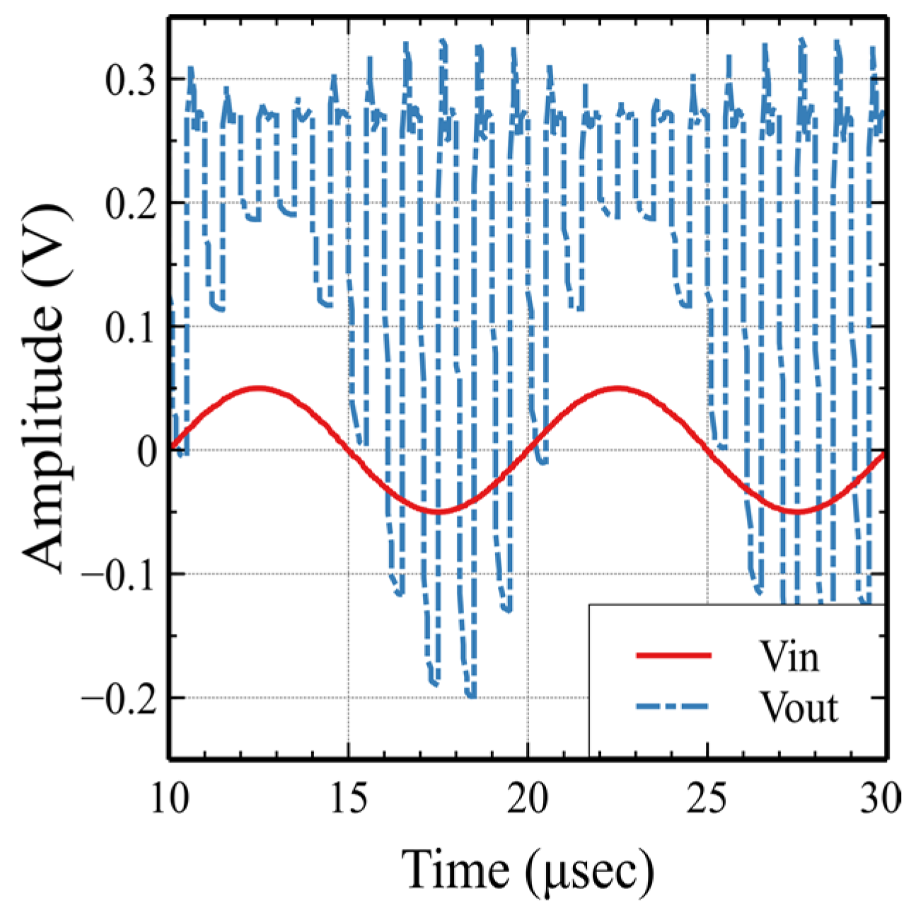
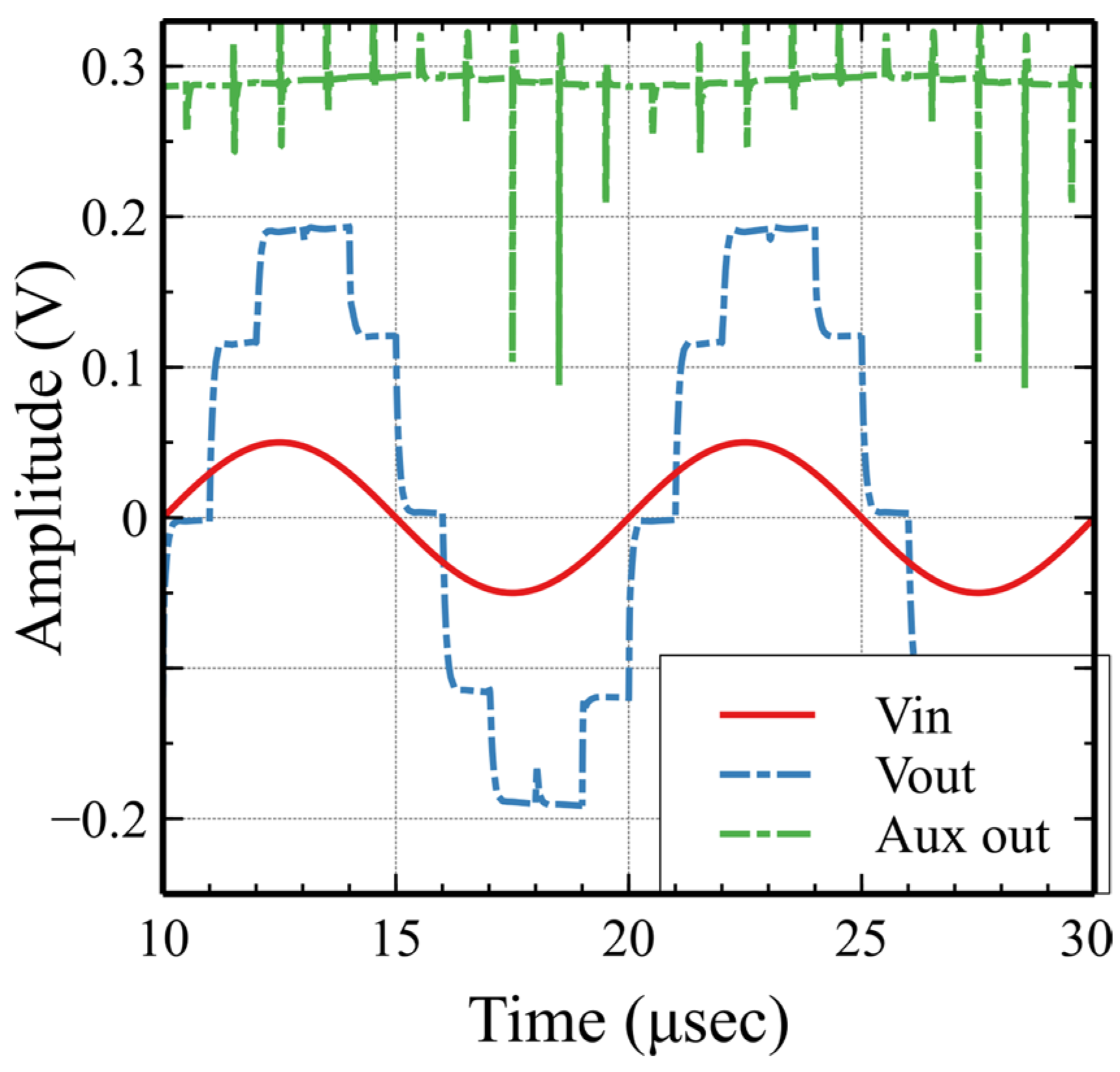
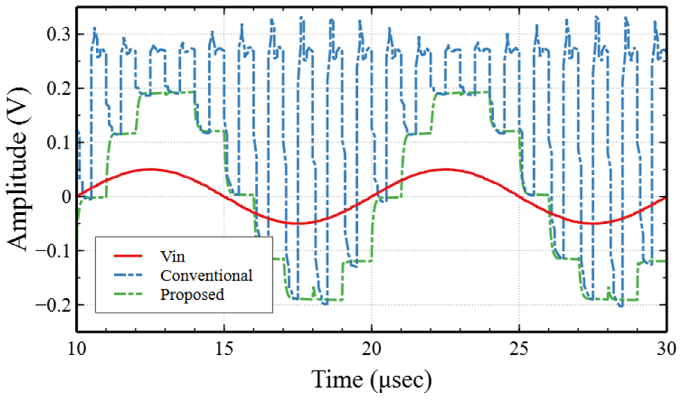
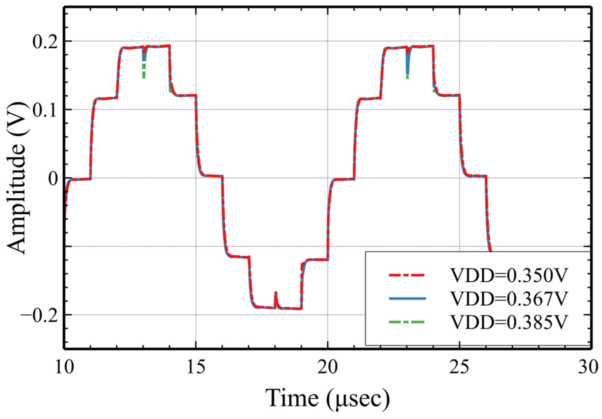
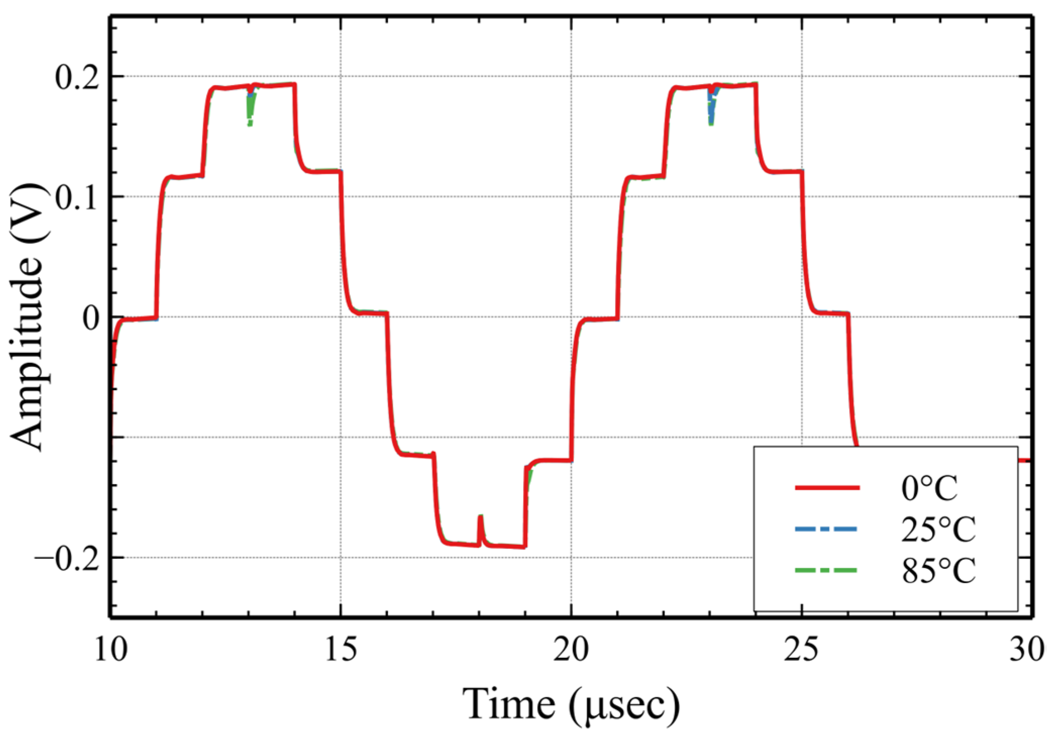
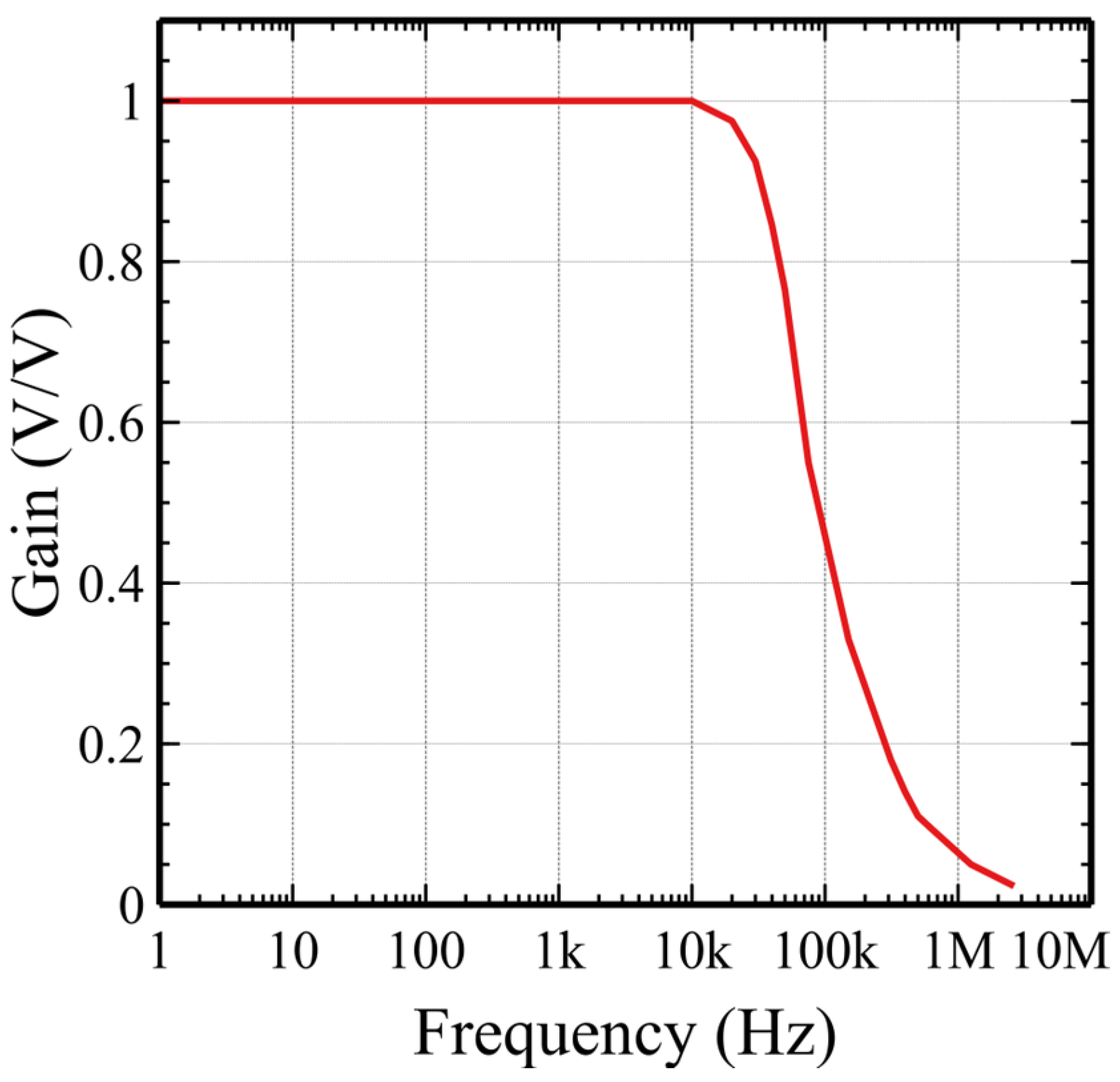
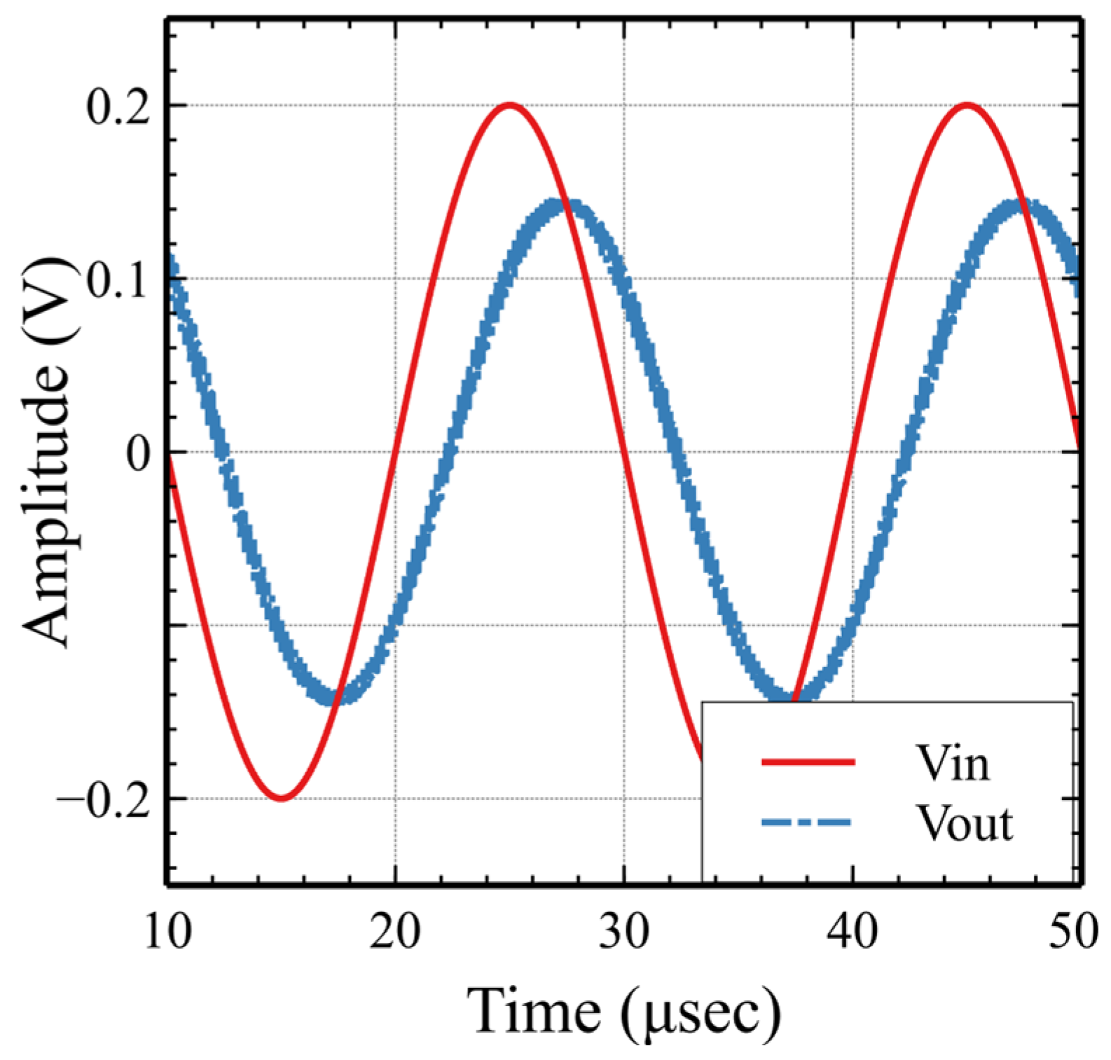
3.1. Low-Voltage SC Amplifier Results

The amplifier was designed for an amplification factor G = Cin/Cf = 4, where Cin = 4 pF and Cf = 1 pF. Figure 9 and Figure 10 show the transient response of conventional low-voltage SC amplifier using a class A Miller op-amp and conventional low-voltage SC amplifier using the enhanced class AB single output Miller op-amp respectively. Figure 11 shows the transient simulation of the proposed low-voltage SC amplifier. For all of these circuits similar input signals a 100 mVpp 100 kHz sinusoidal input, a 1 MHz clock and with an op-amp offset voltage Vos = 30 mV were used. Clock voltage boosting by a factor of two was used [26] to allow switches to operate with rail-to-rail signals and a low supply voltage. The slew rate requirement was highly relaxed as compared to the transient response of the conventional low voltage SC amplifier that uses a class A Miller op-amp; this is depicted in Figure 9. Figure 10 shows the output of the conventional SC amplifier utilizing the proposed GB SR-enhanced AB/AB op-amp with no auxiliary output. The slew rate is improved, but significant distortion is present due to the large slew rate required by the low-voltage operation of the circuit. Simulations of the proposed technique using the enhanced multiple-output Miller op-amp are shown in Figure 11. It can be seen that the output is a true sample and hold signal with no reset to zero or to another constant voltage. The multiple-output technique reduces the slew rate requirements imposed on the op-amp by low-voltage SC circuits. Moreover, it also cancels the 30 mV op-amp input offset voltage. The outputs of the conventional and proposed amplifier are compared in Figure 12, Figure 13, Figure 14 and Figure 15, showing the PVT simulations of the circuit. The design is robust to ss, tt and ff process variations, as well as to 0 °C, 25 °C and 85 °C temperature corners and to supply voltage variations up to 10%.

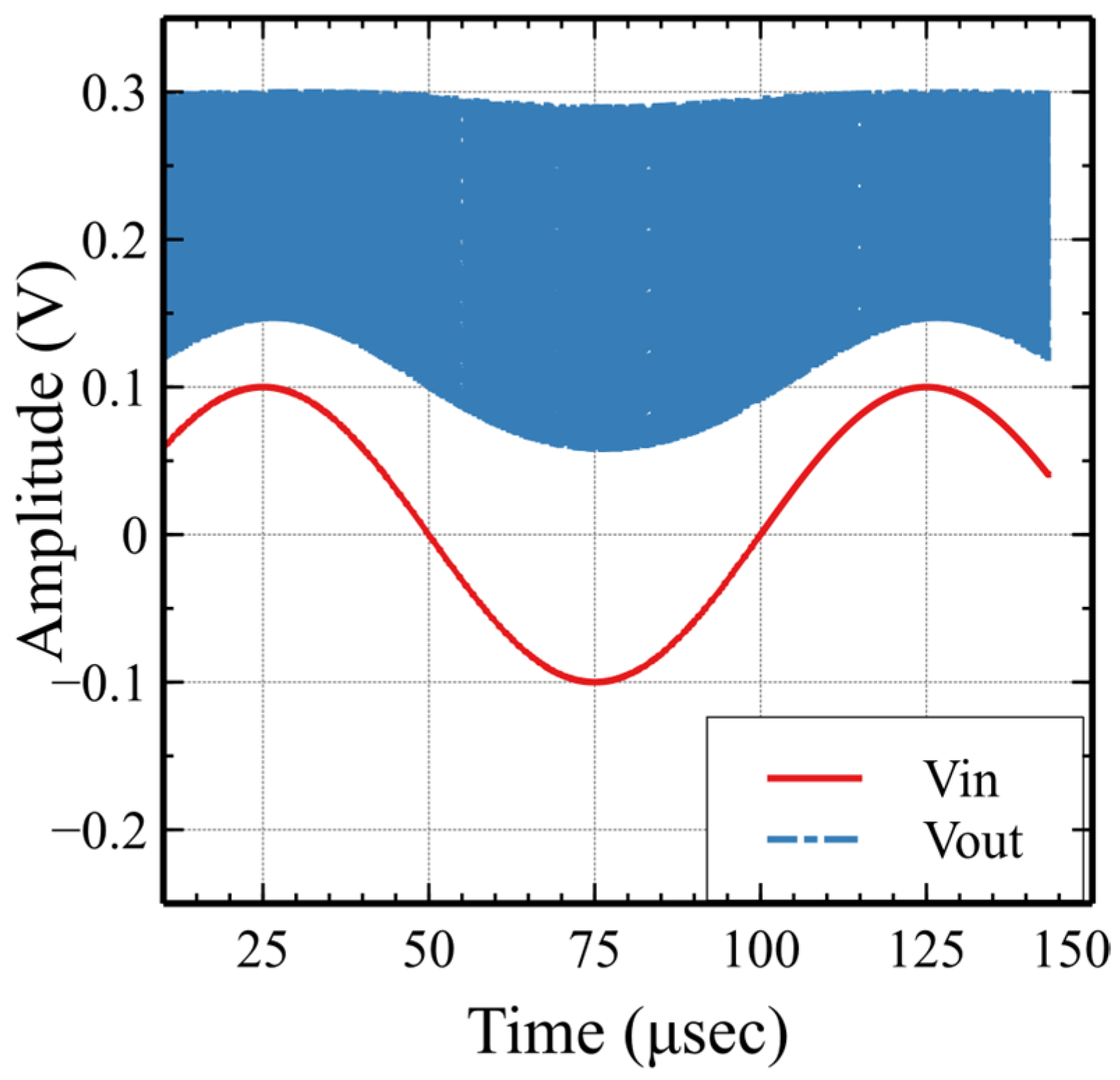
3.2. Low-Voltage SC Low-Pass Filter

The proposed low-pass filter was designed for a cutoff frequency fcutoff = 50 kHz. The circuit is controlled by a non-overlapping clock generator circuit operating with a clock frequency fclk = 5 MHz. The switched capacitors Cin = Cf = 1 pF perform as resistors, with values Rin = Rf = 200 kΩ. On the other hand, a capacitor C = 15.9 pF, in combination with the equivalent resistance value of Cf, yields to the filter’s cutoff frequency fcutoff = 50 kHz. The frequency response of the circuit that was extracted from transient simulations is depicted in Figure 16. The transient simulation of the low-pass filter with a 50 kHz, 400 mVpp input signal with 30 mV DC offset is depicted in Figure 17 for the proposed circuit and in Figure 18 for the conventional implementation. As opposed to the conventional one, the proposed technique cancels out the 30 mV DC offset and the VDDP voltage at the input. Moreover, the conventional SC filter resets every cycle to the voltage VDDP + Vos.

4. Conclusions

A family of low-voltage SC circuits based on multiple-output GB-enhanced class AB/AB op-amps was introduced. The application of this concept was exemplified with a low-pass filter and an amplifier, but it can be easily extended to other SC circuits. The circuits are offset-compensated and capable of operating with dual supply voltages of ±0.35 V anda bias current Ibias = 10 µA in technology with a ±0.9 V nominal supply voltage. The circuits consume 43.4 µW of power. It was verified that the proposed technique is especially appropriate for low-voltage operation, since it essentially relaxes the op-amp slew rate requirements. This is due to the fact that the op-amp signal outputs are true sample and hold signals, which are not subject to a reset phase that requires large output voltage variations. The implementations were validated by the simulation of SC circuits using Cadence Design Framework II and parameters for commercial 180 nm CMOS technology.

Author Contributions

Conceptualization, H.D.R.-A., A.P., J.R.-A., A.L.-M. and R.G.C.; Methodology, H.D.R.-A. and J.R.-A.; Software, J.R.-A.; Validation, H.D.R.-A., A.P. and J.R.-A.; Formal analysis, H.D.R.-A., A.P. and J.R.-A.; Investigation, J.R.-A.; Resources, A.L.-M. and R.G.C.; Writing—original draft, H.D.R.-A., A.P., J.R.-A., A.L.-M. and R.G.C.; Writing—review and editing, H.D.R.-A., A.P., J.R.-A., A.L.-M. and R.G.C. All authors have read and agreed to the published version of the manuscript.

Funding

This research received no external funding.

Data Availability Statement

The original contributions presented in this study are included in the article. Further inquiries can be directed to the corresponding author.

Conflicts of Interest

The authors declare no conflict of interest.

References

  1. Hosticka, B.J.; Brodersen, R.W.; Gray, P.R. MOS sampled data recursive filters using switched capacitor integrators. IEEE J. Solid-State Circuits 1977, 12, 600–608. [Google Scholar] [CrossRef]
  2. Lee, K.-L.; Meyer, R.G. Low-distortion switched-capacitor filter design techniques. IEEE J. Solid-State Circuits 1985, SC-20, 1103–1113. [Google Scholar] [CrossRef]
  3. Nakayama, K.; Kuraishi, Y. Present and future applications of switched-capacitor circuits. IEEE Circuits Devices Mag. 1987, 3, 10–21. [Google Scholar] [CrossRef]
  4. Temes, G.; Moon, U.-K.; Allstot, D. Switched-Capacitor Circuits [Education]. IEEE Circuits Syst. Mag. 2021, 21, 40–42. [Google Scholar] [CrossRef]
  5. Allstot, D.J.; Moon, U.-K.; Temes, G.C. Switched-Capacitor Circuits. In Proceedings of the 2022 IEEE Custom Integrated Circuits Conference (CICC), Newport Beach, CA, USA, 24–27 April 2022; pp. 1–8. [Google Scholar]
  6. Gregorian, R. High-resolution switched-capacitor D/A converter. Microelectron. J. 1981, 12, 10–13. [Google Scholar] [CrossRef]
  7. Temes, G.C.; Haug, K. Improved offset-compensation schemes for switched-capacitor circuits. Electron. Lett. 1984, 20, 508–509. [Google Scholar] [CrossRef]
  8. Cabrera-Bernal, E. Performance Enhancement in the Design of Amplifier and Amplifier-Less Circuits in Modern CMOS Technologies. Ph.D. Thesis, Electronic Engineering Department Higher Technical School of Engineering, University of Seville, Seville, Spain, 18 May 2018. [Google Scholar]
  9. Fiorenza, J.K.; Sepke, T.; Holloway, P.; Sodini, C.G.; Lee, H.S. Comparator-based switched capacitor circuits for scaled CMOS technologies. IEEE J. Solid-State Circuits 2006, 41, 2658–2668. [Google Scholar] [CrossRef]
  10. Chae, Y.; Han, G. Low Voltage, Low Power, Inverter-Based Switched-Capacitor Delta-Sigma Modulator. IEEE J. Solid-State Circuits 2009, 44, 458–472. [Google Scholar] [CrossRef]
  11. Gagliardi, F.; Catania, A.; Piotto, M.; Bruschi, P.; Dei, M. Parallel Slew-Rate Enhancer With Current-Recycling Core for Switched-Capacitors Circuits. IEEE Trans. Circuits Syst. II Express Briefs 2024, 71, 4814–4818. [Google Scholar] [CrossRef]
  12. Roh, J. High-Gain Class-AB OTA with Low Quiescent Current. Analog. Integr. Circuits Signal Process. 2006, 47, 225–228. [Google Scholar] [CrossRef]
  13. Yan, Z.; Mak, P.-I.; Law, M.-K.; Martins, R.P.; Maloberti, F. Nested-Current-Mirror Rail-to-Rail-Output Single-Stage Amplifier With Enhancements of DC Gain, GBW and Slew Rate. IEEE J. Solid-State Circuits 2015, 50, 2353–2366. [Google Scholar] [CrossRef]
  14. Rashtian, M.; Hashemipour, O.; Navi, K. Design of a Low-Voltage High-Speed Switched-Capacitor Filters Using Improved Auto Zeroed Integrator. J. Appl. Sci. 2008, 8, 1771–1775. [Google Scholar] [CrossRef]
  15. Ghasemi, R.; Charkhkar, H.; Asadi, A.; Lotfi, R.; Mafinejad, K. Design of Low-Voltage MOSFET-Only Switched-Capacitor Filters. In Proceedings of the 2005 International Conference on Microelectronics, Islamabad, Pakistan, 13–15 December 2005; pp. 24–29. [Google Scholar]
  16. McCarroll, B.; Sodini, C.; Lee, H.-S. A high-speed CMOS comparator for use in an ADC. IEEE J. Solid-State Circuits 1988, 23, 159–165. [Google Scholar] [CrossRef]
  17. Peluso, V.; Vancorenland, P.; Marques, A.M.; Steyaert, M.S.J.; Sansen, W. A 900-mV low-power Δ∑ A/D converter with 77-dB dynamic range. IEEE J. Solid-State Circuits 1998, 33, 1887–1897. [Google Scholar] [CrossRef]
  18. Bidari, E.; Keskin, M.; Maloberti, F.; Moon, U.; Steensgaard, J.; Temes, G.C. Low-voltage switched-capacitor circuits. In Proceedings of the 1999 IEEE International Symposium on Circuits and Systems (ISCAS), Orlando, FL, USA, 30 May–2 June 1999; pp. 49–52. [Google Scholar]
  19. Dessouky, M.; Kaiser, A. Rail-to-rail operation of very low voltage CMOS switched-capacitor circuits. In Proceedings of the 1999 IEEE International Symposium on Circuits and Systems (ISCAS), Orlando, FL, USA, 30 May–2 June 1999; pp. 144–147. [Google Scholar]
  20. Ramirez-Angulo, J.; Holmes, M. Simple technique using local CMFB to enhance slew rate and bandwidth of one-stage CMOS op-amps. Electron. Lett. 2002, 38, 1409–1411. [Google Scholar] [CrossRef]
  21. Ramirez-Angulo, J.; Carvajal, R.G.; Galan, J.A.; Lopez-Martin, A. A free but efficient low-voltage class-AB two-stage operational amplifier. IEEE Trans. Circuits Syst. II Express Briefs 2006, 53, 568–571. [Google Scholar] [CrossRef]
  22. Pourashraf, S.; Ramirez-Angulo, J.; Lopez-Martin, A.J.; Carvajal, R.G. Super Class-AB OTA without open-loop gain degradation based on dynamic cascode biasing. Int. J. Circuit Theory Appl. (IJCTA) 2017, 45, 2111–2118. [Google Scholar] [CrossRef]
  23. Cabrera-Bernal, E.; Pennisi, S.; Grasso, A.D.; Torralba, A.; Carvajal, R.G. 0.7-V Three-Stage Class-AB CMOS Operational Transconductance Amplifier. IEEE Trans. Circuits Syst. I Regul. Pap. 2016, 63, 1807–1815. [Google Scholar] [CrossRef]
  24. Akbari, M. Single-stage fully recycling folded cascode OTA for switched-capacitor circuits. Electron. Lett. 2015, 51, 977–979. [Google Scholar] [CrossRef]
  25. Abdelfattah, O.; Roberts, G.W.; Shih, I.; Shih, Y.C. An ultra-low-voltage CMOS process-insensitive self-biased OTA with rail-to-rail input range. IEEE Trans. Circuits Syst. I Regul. Pap. 2015, 62, 2380–2390. [Google Scholar] [CrossRef]
  26. Meng, X.; Temes, G.C. Bootstrapping techniques for floating switches in switched-capacitor circuits. In Proceedings of the 2014 IEEE 57th International Midwest Symposium on Circuits and Systems (MWSCAS), College Station, TX, USA, 3–6 August 2014; pp. 398–401. [Google Scholar]
Figure 1. Conventional offset−compensated SC amplifier with a connection to (a) non inverting terminal is connected to a mid-supply voltage for nominal supply operation (shown here as ground potential) or (b) non inverting terminal connected to a voltage VDDP close to one of the rails for low-voltage operation.
Jlpea 15 00024 g001
Figure 2. Conventional offset−compensated SC first−order low-pass filter (a) non inverting terminal is connected to a mid-supply voltage for nominal supply operation (shown here as ground potential) or (b) non inverting terminal connected to a voltage VDDP close to one of the rails for low−voltage operation.
Jlpea 15 00024 g002
Figure 3. Transient response of the low-voltage implementation of SC amplifier of Figure 1 using a conventional op-amp for the gain.
Jlpea 15 00024 g003
Figure 4. Input stage used commonly in Miller op-amps.
Jlpea 15 00024 g004
Figure 5. Gain- and GB-enhanced class AB composite input stage used in the proposed two-output Miller op-amp.
Jlpea 15 00024 g005
Figure 6. Output stages of multiple-output op-amp. (a) Main class AB output stage. (b) Auxiliary class A output stage. (c) Biasing circuit.
Jlpea 15 00024 g006
Figure 7. Proposed low−voltage SC amplifier based on op-amps with two outputs.
Jlpea 15 00024 g007
Figure 8. Proposed low−voltage implementation of an SC low-pass filter using a two-output GB-enhanced Miller op-amp.
Jlpea 15 00024 g008
Figure 9. Transient simulation of the conventional low-voltage SC amplifier using a class A Miller op-amp. The input is a 100 mVpp 100 kHz sinusoidal with a 30 mV op-amp input offset voltage.
Jlpea 15 00024 g009
Figure 10. Transient simulation of the conventional low-voltage SC amplifier using the enhanced class AB single output Miller op-amp. The input is a 100 mVpp 100 kHz sinusoidal input with a 30 mV op-amp input offset voltage.
Jlpea 15 00024 g010
Figure 11. Transient simulation of the proposed low-voltage SC amplifier using a multiple-output enhanced AB/AB Miller op-amp. The input is a 100 mVpp 100 kHz sinusoidal and 30 mV op-amp input offset voltage.
Jlpea 15 00024 g011
Figure 12. Comparison of transient simulations of a conventional low-voltage SC amplifier using the enhanced class AB single-output Miller op-amp and the proposed low-voltage SC amplifier using a dual-output enhanced AB/AB Miller op-amp. The input is a 100 mVpp 100 kHz sinusoidal input with a 30 mV op-amp input offset voltage.
Jlpea 15 00024 g012
Figure 13. Process corner simulation with a 50 mVpp 100 kHz sinusoidal input that has a 30 mV op-amp input offset.
Jlpea 15 00024 g013
Figure 14. Supply voltage corner simulation with a 50 mVp 100 kHz sinusoidal input with a 30 mV offset.
Jlpea 15 00024 g014
Figure 15. Temperature corner simulation with a 50 mVp 100 kHz sinusoidal input that has a 30 mV offset.
Jlpea 15 00024 g015
Figure 16. Frequency response of the low-voltage low-pass SC filter of Figure 8.
Jlpea 15 00024 g016
Figure 17. Low-voltage low-pass filter simulated transient response for a 50 kHz, 400 mVpp sinusoidal input signal with 30 mV input offset for the proposed LV dual-output class AB/AB op-amp with enhanced input stage.
Jlpea 15 00024 g017
Figure 18. Conventional low-voltage low-pass filter simulated transient response for a 50 kHz, 400 mVpp sinusoidal input signal with 30 mV input offset for the LV implementation with single-output class AB op-amp.
Jlpea 15 00024 g018
Table 1. Comparison table.
Parameters[22]
2017
[23]
2016
[24]
2015
[25]
2015
Class AB
Miller Op-Amp
This Work
With Enhanced Class AB Miller Op-Amp
CMOS Tech. Process (nm)1801809065180180
ConfigurationSESE aFD bSE aSE aSE a
Supply (V)±0.90.71.20.35±0.35±0.35
VDDP (V) ---0.270.27
Ibias (uA)14--1010
Isupply (uA)836.28483.33494060
Pdiss (uW)14.525.458017.152843.4
AOLDC (dB)6757.559.1434956
CL (pF)2020532020
CC (pF) 0.58 c-0.6 c22
RC (kOhm) ---1532
SR (V/us)24.111.8115.25.60.89.41
GB (MHz)0.5736503.65.7223
PM (o)826050566345
FOMLS ([V/us*pF/mW])37,30022009909805714376
FOMSS (MHz*pF/mW)9002.3605600630408510,698
FOMGlobal
F O M L S F O M S S
57942278235478515276842
a Single-Ended; b Fully Differential; c Total CC = CC1 + CC2.
Disclaimer/Publisher’s Note: The statements, opinions and data contained in all publications are solely those of the individual author(s) and contributor(s) and not of MDPI and/or the editor(s). MDPI and/or the editor(s) disclaim responsibility for any injury to people or property resulting from any ideas, methods, instructions or products referred to in the content.

