
Full-Bridge DC-DC Converter with Synchronous Rectification Based on GaN Transistors


Abstract
1. Introduction
2. Circuit Structure and Operating Principle of the Converter
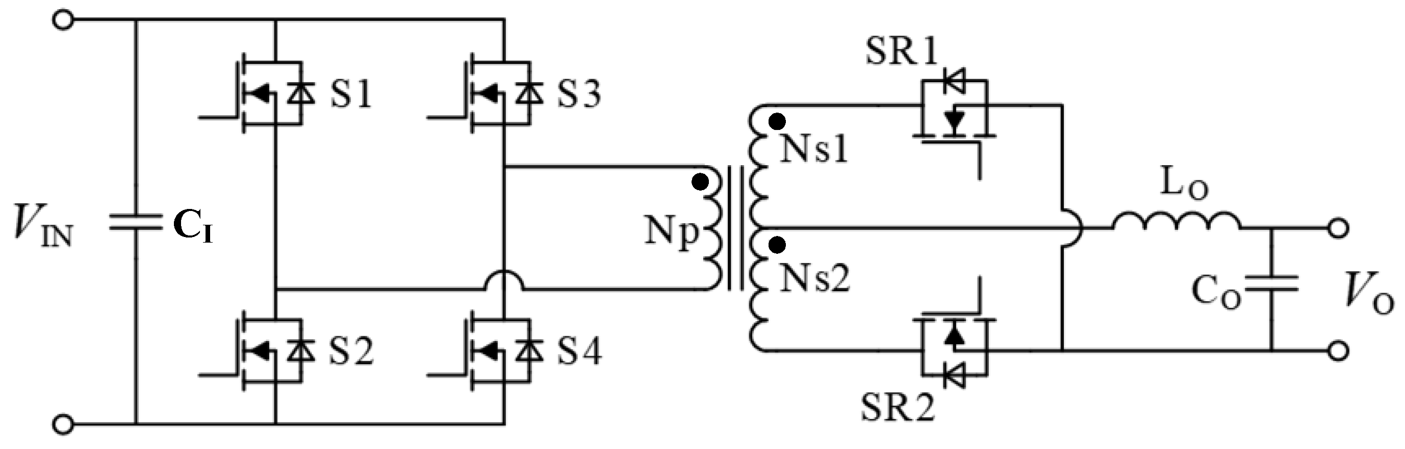
2.1. Proposed Circuit Structure
2.2. Operating Principle of the Main Circuit
- State 1 (t1~t2): Energy Transmission PhaseDuring this phase, the primary-side switches S1 and S4 are turned on, while S2 and S3 remain off. The synchronous rectifier SR1 on the secondary side is conducting, while SR2 is reverse-biased and non-conducting. The input voltage (VIN) is directly applied across the primary winding of the transformer, resulting in negative polarity at the same-name terminal. Energy is transferred from the input to the output, the transformer is magnetized, and the inductor current (ILₒ) increases linearly.
- State 2 (t2~t3): Freewheeling PhaseAt this stage, all primary-side switches (S1 to S4) are turned off, and the voltages across the transformer windings are zero, maintaining constant magnetizing current. The synchronous rectifier SR1 remains on, while SR2 is off. Current flows through the channel of SR1 and the body diode of SR2, ensuring continuity of load current. This phase corresponds to the dead time between S1/S4 and SR2.
- State 3 (t3~t4): Freewheeling PhaseIn this phase, all primary-side switches (S1 to S4) remain off, while both SR1 and SR2 on the secondary side are conducting. The transformer primary and secondary voltages are zero, and the magnetizing current remains unchanged. Current flows simultaneously through the channels of SR1 and SR2, maintaining load continuity.
- State 4 (t4~t5): Freewheeling PhaseAt this stage, all primary-side switches (S1 to S4) remain off, and the transformer primary and secondary voltages remain zero. The synchronous rectifier SR1 turns off, while SR2 remains on. Current flows through the body diode of SR1 and the channel of SR2. This phase corresponds to the dead time between S2/S3 and SR1.
- State 5 (t5~t6): Energy Transmission PhaseDuring this phase, the primary-side switches S2 and S3 are turned on, while S1 and S4 remain off. On the secondary side, SR2 is conducting, while SR1 is reverse-biased and non-conducting. The input voltage (VIN) is directly applied to the primary winding of the transformer, resulting in positive polarity at the same-name terminal. Energy is transferred from the input to the output, the transformer is magnetized, and the inductor current (ILₒ) increases linearly.
- State 6 (t6~t7): Freewheeling PhaseAt this stage, all primary-side switches (S1 to S4) are turned off, and the voltages across the transformer windings are zero, maintaining constant magnetizing current. The synchronous rectifier SR1 is off, while SR2 remains on. Current flows through the body diode of SR1 and the channel of SR2. This phase corresponds to the dead time between S2/S3 and SR1.
- State 7 (t7~t8): Freewheeling PhaseIn this phase, all primary-side switches (S1 to S4) remain off, while both SR1 and SR2 on the secondary side are conducting. The transformer primary and secondary voltages are zero, and the magnetizing current remains unchanged. Current flows simultaneously through the channels of SR1 and SR2, maintaining load continuity.
- State 8 (t8~t9): Freewheeling PhaseDuring this phase, all primary-side switches (S1 to S4) are turned off, and the transformer primary and secondary voltages remain zero. The synchronous rectifier SR1 is conducting, while SR2 is off. Current flows through the channel of SR1 and the body diode of SR2. This phase corresponds to the dead time between S1/S4 and SR2.
- State 9 (t9)At t9, the converter transitions back to state 1, repeating the same sequence for the next switching cycle.
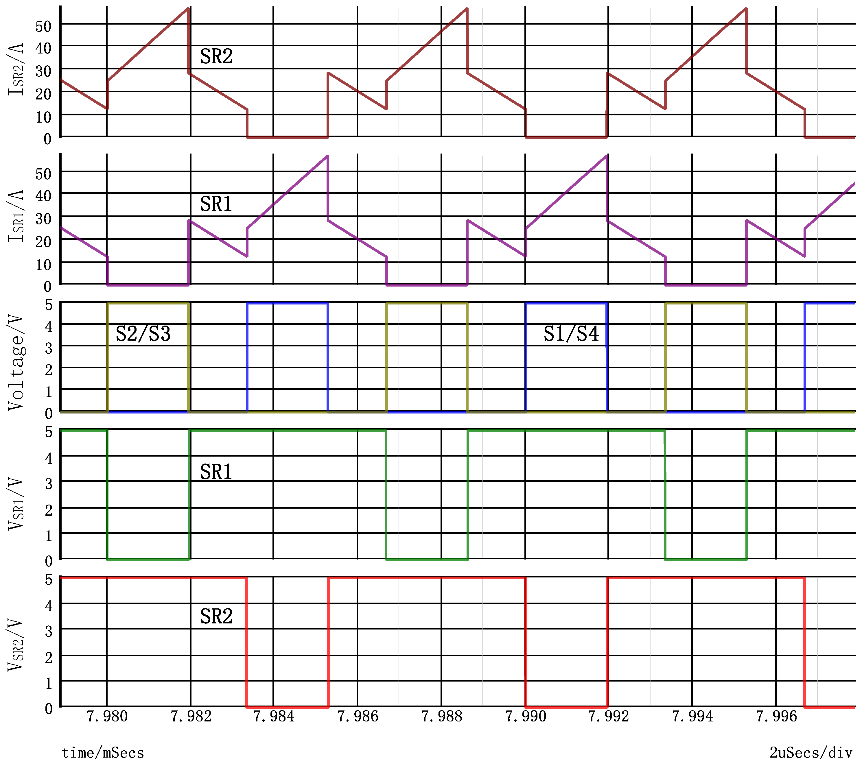
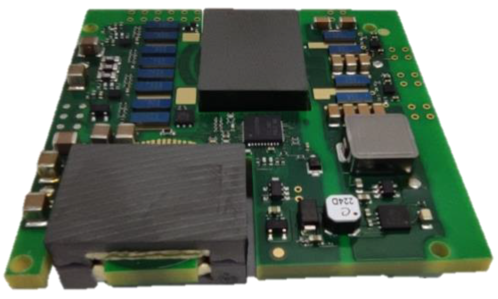
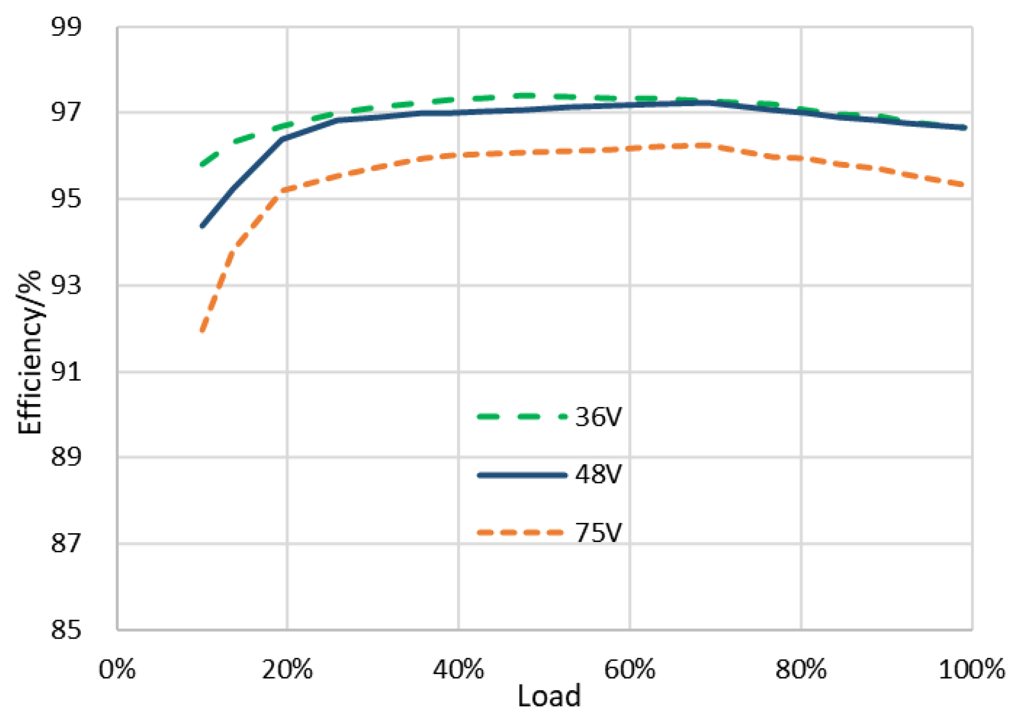
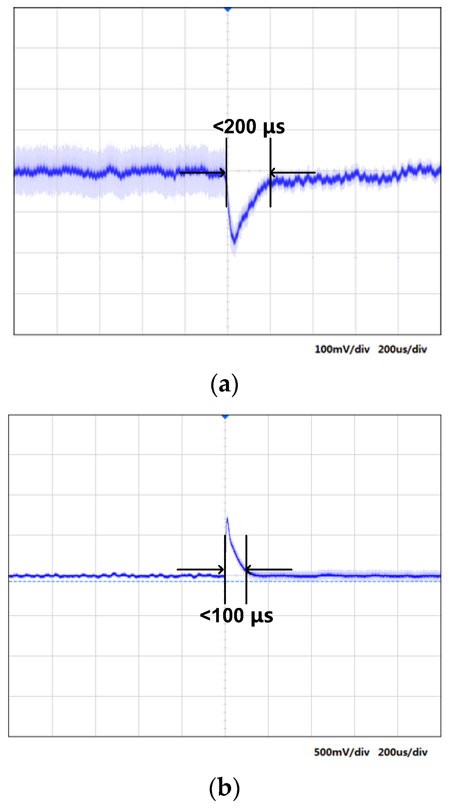
3. Experimental Results
4. Conclusions
Author Contributions
Funding
Data Availability Statement
Conflicts of Interest
References
- Rojas-Dueñas, G.; Riba, J.-R.; Moreno-Eguilaz, M. A Deep Learning-Based Modeling of a 270 V-to-28 V DC-DC Converter Used in More Electric Aircrafts. IEEE Trans. Power Electron. 2022, 37, 509–518. [Google Scholar] [CrossRef]
- Shahzad, D.; Farooq, M.; Pervaiz, S.; Afridi, K.K. A High-Power-Density High-Efficiency Soft-Switched Single-Phase Universal Input to 28-V Isolated AC–DC Converter Module Designed for Paralleled Operation. IEEE Trans. Power Electron. 2022, 37, 8262–8280. [Google Scholar] [CrossRef]
- Shah, F.M.; Xiao, H.M.; Li, R.; Awais, M.; Zhou, G.; Bitew, G.T. Comparative performance evaluation of temperature dependent characteristics and power converter using GaN, SiC and Si power devices. In Proceedings of the 2018 IEEE 12th International Conference on Compatibility, Power Electronics and Power Engineering (CPE-POWERENG 2018), Doha, Qatar, 10–12 April 2018. [Google Scholar]
- Liao, X.; Wang, Y.; Zeng, C.; Li, R.; Chen, Y.; Lai, P.; Huang, Y.; En, Y. Investigation of high-temperature-reverse-bias (HTRB) degradation on AlGaN/GaN HEMTs. In Proceedings of the 2014 IEEE International Conference on Electron Devices and Solid-State Circuits (EDSSC), Chengdu, China, 18–20 June 2014; pp. 1–2. [Google Scholar]
- Chen, H.-Y.; Lin, W.T.; Liao, C.H.; Lin, Z.Y.; Zhang, Z.Q.; Kao, Y.Y.; Chen, K.H.; Lin, Y.H.; Lin, S.R.; Tsai, T.Y. A domino bootstrapping 12 V GaN driver for driving an on-chip 650 V eGaN power switch for 96% high efficiency. In Proceedings of the 2020 IEEE Symposium on VLSI Circuits, Honolulu, HI, USA, 16–19 June 2020; pp. 1–2. [Google Scholar]
- Kao, Y.-Y.; Hung, S.H.; Chen, H.Y.; Lee, J.J.; Chen, K.H.; Lin, Y.H.; Lin, S.R.; Tsai, T.Y. Fully integrated GaN-on-silicon gate driver and GaN switch with temperature-compensated fast turn-on technique for achieving switching frequency of 50 MHz and slew rate of 118.3 V/Ns. IEEE J. Solid-State Circuits 2021, 56, 3619–3627. [Google Scholar] [CrossRef]
- Lin, S.-Y.; Lin, S.Y.; Hung, S.H.; Wang, T.W.; Li, C.H.; Go, C.L.; Huang, S.C.; Chen, K.H.; Zheng, K.L.; Lin, Y.H.; et al. A GaN gate driver with on-chip adaptive on-time controller and negative current slope detector. In Proceedings of the 2023 IEEE International Solid-State Circuits Conference (ISSCC), San Francisco, CA, USA, 19–23 February 2023; pp. 306–308. [Google Scholar]
- Choi, J.; Tsukiyama, D.; Tsuruda, Y.; Davila, J.M.R. High-frequency, high-power resonant inverter with eGaN FET for wireless power transfer. IEEE Trans. Power Electron. 2018, 33, 1890–1896. [Google Scholar] [CrossRef]
- Yan, D.; Ma, D.B. An automotive-use battery-to-load GaN-based switching power converter with anti-aliasing MR-SSM and in-cycle adaptive ZVS techniques. IEEE J. Solid-State Circuits 2021, 56, 1186–1196. [Google Scholar] [CrossRef]
- Yeh, C.-H.; Lin, Y.T.; Kuo, C.C.; Huang, C.J.; Xie, C.Y.; Lu, S.F.; Yang, W.H.; Chen, K.H.; Liu, K.C.; Lin, Y.H. A 70W and 90% GaN-based class-E wireless-powertransfer system with automatic-matching-point-search control for zerovoltage switching and zero-voltage-derivative switching. In Proceedings of the 2018 IEEE International Solid-State Circuits Conference-(ISSCC), San Francisco, CA, USA, 11–15 February 2018; pp. 138–140. [Google Scholar]
- Yang, T.-H.; Wen, Y.H.; Chiu, C.K.; Chen, K.H.; Lin, Y.H.; Lin, S.R.; Tsai, T.Y. A pre-charge tracking technique in the 40 MHz high-speed switching 48-to-5 V GaN-based DC–DC buck converter for reducing large self-commutation loss and achieving a high efficiency of 95.4%. IEEE J. Solid-State Circuits 2022, 57, 2045–2053. [Google Scholar] [CrossRef]
- Chen, Y.; Ma, D.B. A 10-MHz closed-loop EMI-regulated GaN switching power converter using emulated Miller Plateau tracking and adaptive strength gate driving. IEEE J. Solid-State Circuits 2021, 56, 531–540. [Google Scholar] [CrossRef]
- Sebastian, J.; Fernandez, A.; Villegas, P.; Hernando, M.; Prieto, M.J. New topologies of active input current shapers to allow AC-to-DC converters to comply with the IEC-1000-3-2. In Proceedings of the 31st Annual Power Electronics Specialists Conference. Conference Proceedings, Galway, Ireland, 23 June 2000; Volume 2, pp. 565–570. [Google Scholar]
- Kondrath, H. Investigation into Component Losses and Efficiency of a Bidirectional Full-Bridge DC-DC Converter. In Proceedings of the IECON 2018—44th Annual Conference of the IEEE Industrial Electronics Society, Washington, DC, USA, 21–23 October 2018; pp. 1273–1278. [Google Scholar]
- Khodabakhsh, J.; Moschopoulos, G. A Comparative Study of Conventional and T-Type ZVS-PWM Full-Bridge Converters. In Proceedings of the 2018 IEEE Energy Conversion Congress and Exposition (ECCE), Portland, OR, USA, 23–27 September 2018; pp. 6314–6319. [Google Scholar]
- Gu, B.; Lai, J.-S.; Kees, N.; Zheng, C. Hybrid-Switching Full-Bridge DC–DC Converter with Minimal Voltage Stress of Bridge Rectifier, Reduced Circulating Losses, and Filter Requirement for Electric Vehicle Battery Chargers. IEEE Trans. Power Electron. 2013, 28, 1132–1144. [Google Scholar] [CrossRef]
- Bhargavi, P.; Chaganti, P.C.V.; Sowmya, V.; Manitha, P.V.; Lekshmi, S. A Comparative study of Phase shifted Full Bridge and High-Frequency Resonant Transistor DC-DC Converters for EV Charging Application. In Proceedings of the 2022 IEEE 2nd International Conference on Mobile Networks and Wireless Communications (ICMNWC), Tumkur, Karnataka, India, 2–3 December 2022; pp. 1–6. [Google Scholar]
- Lim, C.-Y.; Jeong, Y.; Moon, G.-W. Phase-Shifted Full-Bridge DC–DC Converter with High Efficiency and High Power Density Using Center-Tapped Clamp Circuit for Battery Charging in Electric Vehicles. IEEE Trans. Power Electron. 2019, 34, 10945–10959. [Google Scholar] [CrossRef]
- Wu, H.; Mu, T.; Ge, H.; Xing, Y. Full-Range Soft-Switching-Isolated Buck-Boost Converters with Integrated Interleaved Boost Converter and Phase-Shifted Control. IEEE Trans. Power Electron. 2016, 31, 987–999. [Google Scholar] [CrossRef]
- Landon, T.; Steinbeiser, C.; Page, P.; Hajji, R.; Burgin, G.; Branson, R.; Krutko, O.; Delaney, J.; Witkowski, L. Design of a 600W Doherty using generation 2 HVHBT with 55% WCDMA efficiency linearized to −55dBc for 2c11 6.5dB PAR. In Proceedings of the 2012 IEEE Topical Conference on Power Amplifiers for Wireless and Radio Applications, Santa Clara, CA, USA, 15–18 January 2012; pp. 73–76. [Google Scholar]
- Steinbeiser, C.; Page, P.; Landon, T.; Burgin, G. Doherty Power Amplifiers Using 2nd Generation HVHBT Technology for High Efficiency Basestation Applications. In Proceedings of the 2010 IEEE Compound Semiconductor Integrated Circuit Symposium (CSICS), Monterey, CA, USA, 3–6 October 2010; pp. 1–4. [Google Scholar]
- Takenaka, I.; Ishikura, K.; Takahashi, H.; Hasegawa, K.; Ueda, T.; Kurihara, T.; Asano, K.; Iwata, N. A 330W Distortion-Cancelled Doherty 28V GaAs HJFET Amplifier with 42% Efficiency for W-CDMA Base Stations. In Proceedings of the 2006 IEEE MTT-S International Microwave Symposium Digest, San Francisco, CA, USA, 11–16 June 2006; pp. 1344–1347. [Google Scholar]
- Chandrashekar, K.; Ashwini, U. Dual Channel C-Band Solid State Power Amplifier for Unmanned Aerial Vehicles. In Proceedings of the 2024 International Microwave and Antenna Symposium (IMAS), Marrakech, Morocco, 21–23 October 2024; pp. 1–5. [Google Scholar]
- Gagan, M.N.; Usha, A.; Jagadeesh, S.; Singh, B.K.; Chippalkatti, V.S. Design and implementation of pulsed output interleaved flyback converter with lossless snubber and current mode control. In Proceedings of the 2017 International Conference on Smart grids, Power and Advanced Control Engineering (ICSPACE), Bangalore, India, 17–19 August 2017; pp. 53–58. [Google Scholar]
- Dragon, C.; Brakensiek, W.; Burdeaux, D.; Burger, W.; Funk, G.; Hurst, M.; Rice, D. 200W push-pull & 110W single-ended high performance RF-LDMOS transistors for WCDMA basestation applications. In Proceedings of the IEEE MTT-S International Microwave Symposium Digest, 2003, Philadelphia, PA, USA, 8–13 June 2003; Volume 1, pp. 69–72. [Google Scholar]
- Noh, G.; Lim, G.C.; Ha, J.I. Analysis of Synchronous-Rectification Switch Control for Active Class-E Rectifier. In Proceedings of the 2021 IEEE Energy Conversion Congress and Exposition (ECCE), Vancouver, BC, Canada, 10–14 October 2021; pp. 2059–2066. [Google Scholar]
- Shen, J.; Jing, L.; Qiu, J. High-frequency Full-bridge 48V DC-5V DC LLC Resonant Converter with AlGaN/GaN HEMTs. In Proceedings of the 2023 5th International Conference on Electrical Engineering and Control Technologies (CEECT), Chengdu, China, 15–17 December 2023; pp. 338–342. [Google Scholar]
- Zambetti, O.; Colombo, M.; D’angelo, S.; Saggini, S.; Rizzolatti, R. 48V to 12V isolated resonant converter with digital controller. In Proceedings of the 2017 IEEE Applied Power Electronics Conference and Exposition (APEC), Tampa, FL, USA, 26–30 March 2017; pp. 315–321. [Google Scholar]
- Li, M.; Ouyang, Z.; Andersen, M.A.E. A Hybrid Multitrack-Sigma Converter with Integrated Transformer for Wide Input Voltage Regulation. In Proceedings of the 2020 IEEE Applied Power Electronics Conference and Exposition (APEC), New Orleans, LA, USA, 15–19 March 2020; pp. 1844–1850. [Google Scholar]
- Fu, M.; Fei, C.; Yang, Y.; Li, Q.; Lee, F.C. A Two-Stage Rail Grade DC/DC Converter Based on GaN Device. In Proceedings of the 2019 IEEE Applied Power Electronics Conference and Exposition (APEC), Anaheim, CA, USA, 17–21 March 2019; pp. 2110–2114. [Google Scholar]


| Parameter | Model/Value |
|---|---|
| S1–S4 | EPC2032 |
| SR1–SR2 | EPC2034 |
| Transformer | ER28/10/20 |
| LO | ER25/10/18 |
| CI | 25 μF |
| CO | 200 μF |
| Parameter | Value |
|---|---|
| Rated Input Voltage | 48 V |
| Input Voltage Range | 36–75 V |
| Output Voltage | 28 V |
| Output Current | 42 A |
| Output Voltage Ripple | Vpp < 100 mV |
| Switching Frequency | 300 kHz |
| Size | 2.4 in × 2.28 in × 0.5 in |
| Ref. | [27] | [28] | [29] | [30] | This Work |
|---|---|---|---|---|---|
| Frequency | 1 MHz | 250 kHz | 800 kHz | 200 kHz/2 MHz | 300 kHz |
| Input Range | 48 V | 48 V | 32–75 V | 64–160 V | 36–75 V |
| Output Voltage | 5 V | 12 V | 5 V | 24 V | 28 V |
| Peak Efficiency | 96.6% | 96.4% | 95.1% | 95.1% | 97.1% |
| Full-Load Efficiency | 91.8% | / | / | / | 96.6% |
| Output Power | 250 W | 600 W | 100 W | 200 W | 1176 W |
| Power Density | / | / | 190 W/in3 | 130 W/in3 | 430 W/in3 |
Disclaimer/Publisher’s Note: The statements, opinions and data contained in all publications are solely those of the individual author(s) and contributor(s) and not of MDPI and/or the editor(s). MDPI and/or the editor(s) disclaim responsibility for any injury to people or property resulting from any ideas, methods, instructions or products referred to in the content. |
© 2025 by the authors. Licensee MDPI, Basel, Switzerland. This article is an open access article distributed under the terms and conditions of the Creative Commons Attribution (CC BY) license (https://creativecommons.org/licenses/by/4.0/).
Share and Cite
Wang, X.; Zhao, Q.; Zhao, Z.; Meng, F. Full-Bridge DC-DC Converter with Synchronous Rectification Based on GaN Transistors. J. Low Power Electron. Appl. 2025, 15, 25. https://doi.org/10.3390/jlpea15020025
Wang X, Zhao Q, Zhao Z, Meng F. Full-Bridge DC-DC Converter with Synchronous Rectification Based on GaN Transistors. Journal of Low Power Electronics and Applications. 2025; 15(2):25. https://doi.org/10.3390/jlpea15020025
Chicago/Turabian StyleWang, Xin, Qingsong Zhao, Zenglong Zhao, and Fanyi Meng. 2025. "Full-Bridge DC-DC Converter with Synchronous Rectification Based on GaN Transistors" Journal of Low Power Electronics and Applications 15, no. 2: 25. https://doi.org/10.3390/jlpea15020025
APA StyleWang, X., Zhao, Q., Zhao, Z., & Meng, F. (2025). Full-Bridge DC-DC Converter with Synchronous Rectification Based on GaN Transistors. Journal of Low Power Electronics and Applications, 15(2), 25. https://doi.org/10.3390/jlpea15020025