Review

3D Integrated DNN Accelerators: Recent Trends and Future Prospects

by
Abrar Abdurrob
1,†,
Aristotelis Tsekouras
2,†,
Evangelos Tzouvaras
2,†,
Vasilis F. Pavlidis
2 and
Emre Salman
1,*
1
Department of Electrical and Computer Engineering, Stony Brook University (SUNY), Stony Brook, NY 11794, USA
2
Department of Electrical and Computer Engineering, Aristotle University of Thessaloniki, 541 24 Thessaloniki, Greece
*
Author to whom correspondence should be addressed.
These authors contributed equally to this work.
J. Low Power Electron. Appl. 2026, 16(2), 21; https://doi.org/10.3390/jlpea16020021
Submission received: 27 April 2026 / Revised: 9 June 2026 / Accepted: 11 June 2026 / Published: 18 June 2026
(This article belongs to the Special Issue 15th Anniversary of Journal of Low Power Electronics and Applications)

Abstract

The rapid growth of Deep Neural Networks (DNNs) has led to the development of application-specific DNN accelerators. Conventional 2D von Neumann architectures suffer from memory bandwidth limitations between the memory and the processing core. 3D DNN accelerators have emerged as a promising solution by leveraging 3D integration to enable near-memory logic or in-memory computation. By shifting computation closer to memory, these accelerators significantly reduce data movement and therefore latency, resulting in more energy-efficient operations. Monolithic 3D (M3D) integration, in particular, enables high-bandwidth systems by utilizing high-density monolithic inter-tier vias (MIVs). This paper provides a critical review of recent advances in 3D DNN accelerators that combine near-memory and compute-in-memory with various 3D technologies, offering a useful discussion and future prospects of the available technologies and architectures that have advanced the performance of DNN accelerators. Particular attention is devoted to accelerators for emerging transformer-based large language model (LLM) networks due to the higher memory demands. Thermal-aware design techniques of 3D DNN accelerators are also discussed as a means to address the fundamental challenge of heat dissipation. A detailed review is finally conducted on package-level constraints, considering signal integrity, power delivery, and thermo-mechanical reliability.

1. Introduction

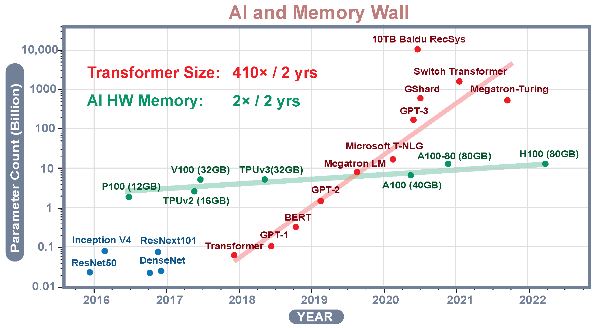
Deep Neural Networks (DNNs) have undergone explosive growth in scale and complexity in the past few years due to their potential in applications such as computer vision [1], natural language processing (NLP) [2], and autonomous vehicles [3], as shown in Figure 1. This growth has accelerated with the rise of transformer-based architectures, where large language models (LLMs) with hundreds of billions of parameters have become the dominant workload driving AI hardware demands [4]. Unlike earlier convolutional models, transformers impose substantially higher memory bandwidth and capacity requirements, further widening the gap between computational demand and available memory throughput [4]. However, memory bandwidth has increasingly become a constraint due to the delay and energy overhead of data movement. To overcome this bottleneck, 3D stacked memory architectures, such as memory-on-logic, compute-in-memory (CIM), and monolithic 3d (M3D) integration have been proposed. These 3D technologies also enable the heterogeneous integration of emerging memory structures such as resistive and ferroelectric memory [5].
Before describing specific 3D integration strategies, the terminology surrounding compute-near-memory architectures is worth clarifying since the relevant terms are not always used consistently in the literature. Throughout this paper, Near-Data Processing (NDP) is used as the umbrella term for any architecture that locates compute close to memory rather than on a separate host die. Processing-Near-Memory (PNM) refers to the specific case where compute resides on a logic die underneath or beside a stacked memory, as in the HMC (Hybrid Memory Cube)- and HBM (High-Bandwidth Memory)-based systems reviewed in Section 2.1. Processing-in-memory (PIM) refers to compute logic embedded inside a memory tier, and compute-in-memory (CIM) refers to the narrower case in which the memory bitcell array itself performs multiply-accumulate (MAC) operations, as in the ReRAM and SRAM-based designs of Section 2.2.
Stacking memory on a logic die has been the most widely used approach for NDP, whereas CIM has recently gained significant attention. The main difference between the two methods is the presence of processing units in memory: in NDP applications, processing occurs in close proximity to the memory, thus reducing the transfer distance of the data, while in CIM processing occurs within the memory, almost eliminating data transfer [6]. Two prominent memory-on-logic systems, depending upon the memory utilized, have appeared in industry: HBM by AMD [7] and HMC by Micron [8]. HMC utilizes multiple vertically stacked DRAM dies partitioned into a 2D grid, with the vertical die partitions comprising a “vault.” Each vault is controlled by a dedicated controller on the logic die. In contrast, HBM utilizes horizontally partitioned DRAM stacks, treating different memory layers as distinct channels. Communication between layers is achieved by through silicon vias (TSVs) [9]. HBM has since become the prevailing memory technology for AI accelerators, with successive generations (e.g., HBM3 and HBM3E), delivering per-stack bandwidths exceeding 800 GB/s and being deployed in commercial platforms such as the AMD Instinct MI300 series [10].
M3D technology is another technique that offers a promising path to achieving significantly higher densities for complex DNN models with a large number of parameters [11]. An M3D system consists of multiple tiers that are vertically formed on the same silicon substrate. The tiers are separated with thin dielectric structures, the Inter-Layer Dielectric (ILD). The connection between the different tiers is performed with the monolithic inter-tier vias (MIVs). The MIVs have a significantly lower diameter (≈50 nm) in comparison with TSVs (≈5 μ m) [12]. Even though M3D technology offers more energy-efficient and higher density interconnects between the memory and logic layers, this technology still faces specific fabrication challenges and is not as mature as the TSV technology [13].
Thermal management is a common challenge across all the discussed 3D technologies [14,15], and therefore thermal-aware design is crucial for the efficient operation of 3D systems. The high computational demands in 3D technologies can lead to significant thermal issues that degrade reliability, particularly under coupled thermal and mechanical stresses [16]. Increased density and power consumption require the adoption of several strategies, which often involve advanced cooling techniques [17], partitioning methods [18], or thermal-aware design such as system-level parameter optimization [19] to prevent overheating.
The three categories of 3D integration discussed above (memory-on-logic, compute-in-memory, and monolithic 3D) are sometimes presented as parallel alternatives, but they address different bottlenecks and sit at different levels of the design hierarchy. Memory-on-logic is best understood as an integration strategy: it pairs commodity 3D-stacked memory with a dedicated logic die. CIM, by contrast, is a computing paradigm in which MAC operations are executed inside the memory array or close enough to it that the data-movement cost is negligible. In contrast, M3D systems represent an emerging fabrication and interconnect technology that enables vertical integration at MIV pitch with tier-level granularity. These three approaches are not mutually exclusive, and several of the heterogeneous designs discussed later in this paper combine two or three of them in a single stack. In Table 1, a comparison between the different 3D integration categories is performed in terms of the bottlenecks they address, their key advantages and limitations. For each category, the maturity level is also reported, and representative state-of-the-art architectures are highlighted.
The rest of the paper is organized as follows. An overview of existing 3D (NDP, CIM, and M3D) DNN accelerators is provided in Section 2 with emphasis on advances in energy efficiency and limitations, while special attention is given to accelerators with transformer, LLM-based workloads. Thermal-aware design methodologies for 3D DNN accelerators are summarized in Section 3. The different package-level topologies for these devices are analyzed in Section 4, along with their implementation constraints. Finally, the paper is concluded in Section 5 by reviewing the maturity level of 3D DNN implementations, and by summarizing the future prospects.

2. Vertical Integration for DNN Accelerators

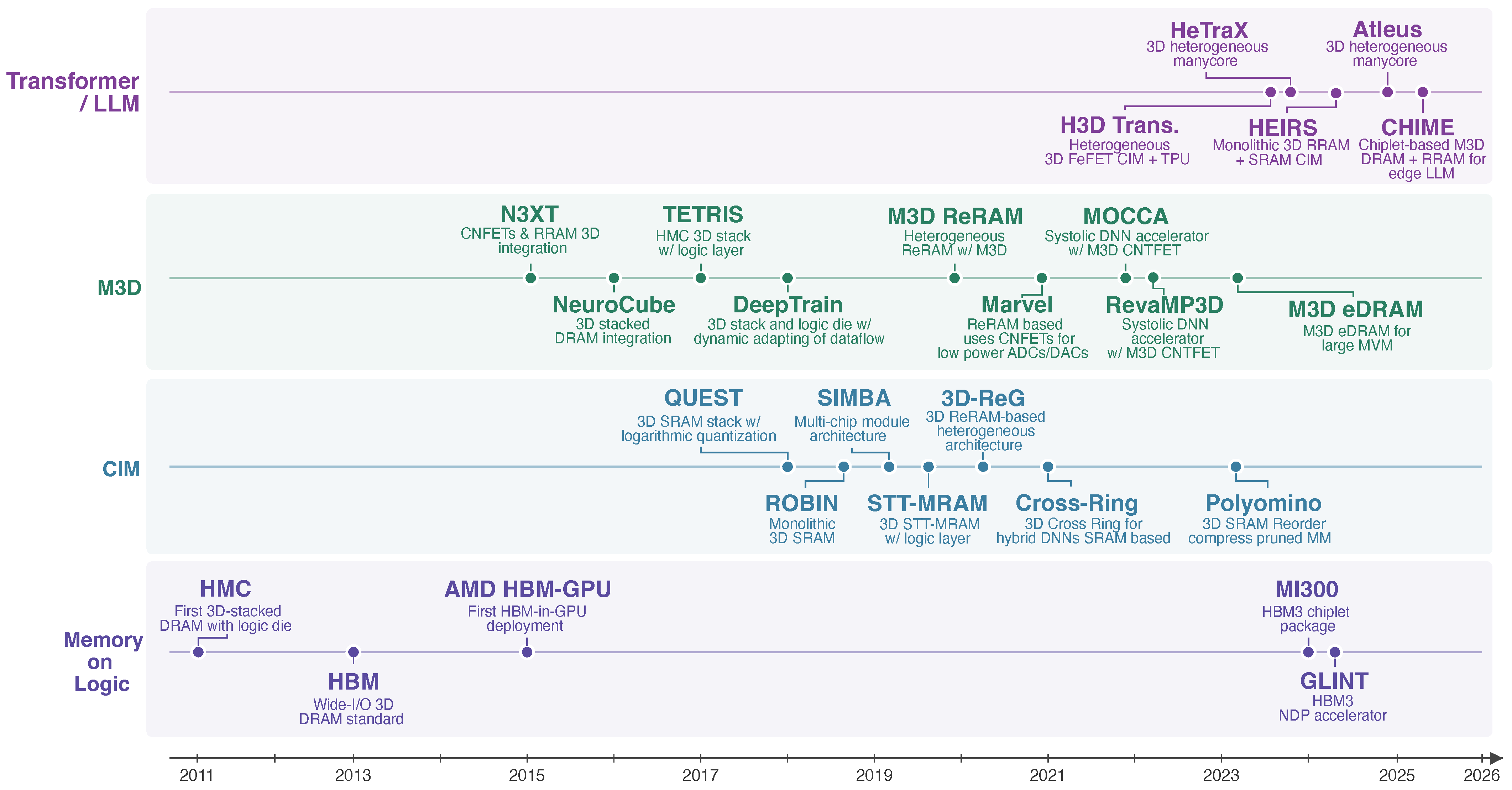
This section is focused on memory-on-logic, CIM, and M3D implementations for 3D DNNs. The timeline of developments is shown in Figure 2, where the innovations of HMC and HBM set the foundation of future advancements.

2.1. Memory-on-Logic 3D DNN Accelerators

The landscape of memory-on-logic systems for DNN accelerators is investigated in this subsection. According to the literature, the parallel memory access capabilities of HMC have been suitable for many early DNN applications focusing on NDP [20]. Hence, this subsection begins with HMC-based memory-on-logic implementations, followed by SRAM-based systems and more recent HBM-based architectures.
HMC implementations have been used in multiple 3D DRAM architectures. Neurocube [20,34] has been one of the first DRAM-based accelerators built on HMC that comprises multiple DRAM dies stacked on a logic die. The processing element (PE) clusters are contained in the logic die, connected through a 2D NoC. Since Neurocube’s architecture has not been fully optimized, CIM could provide additional opportunities for improvement. Performance is reported solely through architectural simulation of the logic tier at 28 nm and 15 nm, and the workload consists of the convolutional network inference and the training phase [20]. TETRIS [21,34] also follows the HMC approach with differentiating features from Neurocube. In TETRIS, the architecture is rebalanced by increasing the area allocated to the PEs while reducing the area allocated to the SRAM buffers, resulting in higher throughput. TETRIS reduces energy consumption by 1.5× compared to 2D DNN conventional accelerators, with the comparison focusing the architectural simulation on a CNN workload [21].
Figure 2. Chronological timeline of primary developments in 3D DNN accelerators, organized into four technology threads. The memory-on-logic lane (indigo) tracks the commercial 3D-stacked DRAM path from HMC (2011) [8] and HBM (2013) [7] through the AMD MI300 (2024) [10] and the HBM3-based GLINT NDP accelerator [24]. The CIM lane (blue) captures the rise of in-memory MAC operations across SRAM (QUEST [23], ROBIN [35]), DRAM-class (SIMBA [36]), and emerging-NVM (STT-MRAM [25], 3D NAND [26], ReRAM [37]) substrates between 2018 and 2023, including the silicon test chip Polyomino [38]. The M3D lane (green) follows monolithic 3D integration from the N3XT foundation (2015) [28] through CNTFET-based accelerators (Marvel [30] and MOCCA [31]), heterogeneous ReRAM M3D systems [32], and the RevaMP3D [33] core and cache redesign over N3XT. The Transformer/LLM lane (purple) tracks the most recent line of work, with heterogeneous 3D architectures (H3DAtten [1], H3D-Transformer [39], HeTraX [40], HEIRS [27], Atleus [41], and CHIME [42]) appearing in rapid succession from 2023 onward in response to the bandwidth and capacity demands of transformer inference.
Jlpea 16 00021 g002
The DeepTrain architecture [22] uses the same compute and memory units for all kernels but dynamically adapts the dataflow. The smaller dataset is replicated, while the larger dataset is partitioned across all PEs, requiring a communication fabric with a broadcast bus and unicast connections. DeepTrain achieves over 10× higher efficiency compared to Neurocube, but its performance is limited by off-chip latency, which the original work identifies only through architecture-level simulation of the training phase [22].
QeiHaN [43] is another implementation of an HMC accelerator focusing on logarithmic quantization activations and a weight storage scheme. Logarithmic quantization is a technique commonly employed in DNNs to reduce the precision of the activation and weight parameters. As such, a quantization unit is placed within the accelerator, without contributing substantially to the overall area or energy dissipation. Input activations are distributed channel-wise across vaults, while each vault stores a portion of the partial outputs for all channels. The weights are also distributed channel-wise, with bits interleaved across banks within a vault. In this way, QeiHaN achieves 3.5× less energy consumption compared to Neurocube. However, this comparison is based on architectural simulations of CNN inference workloads, while the accuracy impact of logarithmic quantization remains a separate trade-off that must be evaluated for the target model.
The main drawback of HMC-based designs is that DRAM-based memory tiers further constrain the energy budget due to the additional refresh power and access latency. Multiple implementations have also utilized 3D-stacked SRAM to achieve lower latencies and to eliminate DRAM refresh energy from the budget, enabling fast access to the DNN parameters for quicker inference. For instance, QUEST [23] utilizes a stack of eight SRAM dies on a processing chip with 24 cores. The accelerator is split into vaults similarly to the HMC, with the SRAMs and the cores communicating via an inductive coupling technology called ThruChip Interfaces (TCI) [44]. QUEST also utilizes logarithmic quantization, achieving an energy efficiency of 877 GOPS/W. Unlike most accelerators discussed in this section, QUEST is a fabricated silicon prototype in 40 nm CMOS; therefore, the reported efficiency reflects measured silicon implementation [23].
MAESTRO [45] consists of a single memory die stacked on logic, divided into a grid of 64×64 blocks, with an intermediate switch die. The switch die consists of H-trees implemented across different metal layers, along with selection blocks that route data to the appropriate H-tree and combining blocks that merge multiple inputs before sending them to the SRAM die. Although MAESTRO achieves high energy efficiency compared to DRAM designs, additional area for the H-trees is required. The reported metrics are derived from circuit-level layout and analytical performance modeling of CNN inference, rather than from a fabricated implementation [45].
In Ref. [46], a 3D cross-ring accelerator is designed that includes four 3D-SRAM stacks on a single logic die. The system communicates with external DRAM through a controller implemented on the logic die. The cross-ring architecture uses vertical and horizontal rings linking a PE cluster with an SRAM cube through simplified micro-routers, designed for energy-efficient data movement. Compared to Eyeriss [47], Cross-Ring achieves up to 17.4× lower energy consumption. This metric is obtained from architectural simulation on hybrid DNN workloads. The overhead of off-chip DRAM accesses is not included [46].
Finally, a matrix reordering technique for a 3D-SRAM Polyomino accelerator is proposed in [38]. The process prioritizes columns with the highest non-zero rates, then groups rows into sets aiming for a consistent number of non-zero elements per column within each set. This structure further leverages the effective storage of reordered sparse matrices through a new format called a Compressed Reordered Sparse Matrix (CRSM), which reduces memory usage by 63%, thus achieving higher area and energy efficiency compared to DRAM-based systems. Polyomino has been fabricated in 180 nm CMOS targeting randomly pruned matrix multiplication, and the reported area and energy savings are measured on a silicon prototype using sparse-DNN workloads [38].
While the HMC- and SRAM-based accelerators discussed above have advanced the energy efficiency and throughput of 3D DNN accelerators, industry adoption has increasingly converged on High-Bandwidth Memory (HBM) as the primary 3D stacked memory technology for AI workloads due to offering both the capacity needed for billion-parameter models and a standardized package-level interface that can be easily integrated into mainstream foundry flows compared to academic 3D-SRAM and HMC stack implementations. HBM offers higher per-stack bandwidth and capacity compared to HMC, and successive generations have scaled to meet the growing demands of transformer and LLM inference. For example, an HBM3-based NDP accelerator is proposed in [24] that addresses the area, dataflow, and thermal constraints of near-data processing through a hardware-software co-design approach, leveraging the multi-channel data organization of HBM3 to improve throughput while remaining within the area constraints of the logic die; this work is also focused on the architectural level.
While the HBM-attached accelerators accommodate the bandwidth and capacity needs for the transformer inference, the workload can consist of a mix of static weights and dynamic-operand operations that cannot be served efficiently by a single memory technology. More recently, the rise of transformer-based workloads has motivated the development of heterogeneous 3D architectures that combine multiple memory and compute technologies within a single vertically integrated stack. H3D-Transformer [39] adopts an interposer substrate with multiple 3D memory/logic hybrid cubes, each optimized for different matrix multiplication workloads present in transformer models. By combining FeFET-based mixed-signal compute-in-memory (CIM) cubes with digital tensor processing unit (TPU) cubes, H3D-Transformer achieves approximately 10 TOPS/W energy efficiency on BERT and GPT-2 models, representing a 2.6× to 3.1× improvement over a baseline with a 7 nm TPU and stacked FeFET memory [39]. The performance comparison is made against a same-technology FeFET baseline rather than a general-purpose GPU or a 2D ASIC. The improvement source is the workload-aware partitioning between mixed-signal FeFET CIM, which handles the static W Q , W K , W V and feed-forward network (FFN) weight matrix-vector multiplications (MVMs) and the digital TPU tile, which handles the dynamic attention scores, so the 10 TOPS/W metric refers to the system-level efficiency of that partition. Furthermore, FeFET arrays have not yet been demonstrated in full-scale production, and the temperature sensitivity of FeFET retention would necessitate appropriate thermal management.
HeTraX [40] is another heterogeneous 3D manycore architecture that aligns specialized hardware resources across 3D tiers with the diverse computational kernels of transformer models, achieving up to 5.6× speed-up and 14.5× energy-delay product improvement while maintaining thermal feasibility. Atleus [41] extends this line of work to support both transformer fine-tuning and inference on a 3D platform utilizing ReRAM tiers for weight storage and systolic array tiers for dynamic computations. Pre-trained weights are stored on the non-volatile ReRAM cores, enabling energy-efficient multi-task deployment where only the lightweight adapter parameters need to be updated across different tasks [41]. These heterogeneous 3D approaches represent a change from the single-memory-technology paradigm of earlier memory-on-logic accelerators and highlight the growing importance of workload-aware vertical integration. Both HeTraX and Atleus rely on the same architecture-level evaluation as H3D-Transformer. HeTraX reports improvements using an integrated thermal model to justify thermal feasibility but assumes that the M3D manycore substrate is realizable at the targeted density. The benefits of Atleus are derived from algorithmic improvements, specifically by holding pre-trained weights fixed and updating only adapter parameters across tasks, which is a workload-based argument, independent of the 3D substrate.
Overall, the memory-on-logic accelerators presented in this subsection illustrate a consistent pattern. The HMC- and SRAM-based designs (i.e., Neurocube, TETRIS, DeepTrain, QeiHaN, MAESTRO, and Cross-Ring) report large speed-ups and energy savings over 2D baselines, but the comparisons focus on the architectural-level simulations of the respective 2D accelerator for a similar workload. Hence, the benefits are dominated by the bandwidth and energy gains of the vertical interconnects instead of any architectural innovations specific to the proposed designs. The two silicon prototypes (i.e., QUEST and Polyomino) are exceptions to this pattern. Their fabrication is achieved at older technology nodes, 40 nm and 180 nm respectively. The authors report measured instead of projected energy; hence, the reported energy metrics are more modest compared to the simulation-based designs. The heterogeneous transformer architectures (i.e., H3D-Transformer, HeTraX, and Atleus) and the HBM3-based NDP work focus on modern workloads, but they remain at the simulation level and depend on device assumptions (e.g., FeFET endurance, M3D yield, and HBM thermal envelope), whose worst-case behavior has not been characterized yet. A fair summary is that memory-on-logic is the most commercially mature of the three categories presented in this paper, with HBM-attached accelerators already in production. Another important consideration is how interconnect and I/O costs are modeled. Some of the works above include TSV channel energy and refresh power for the HMC stack in their energy budget (i.e., Neurocube, DeepTrain); however, other works only consider the logic die and treat the memory access as ideal (e.g., several SRAM-stacked designs), while the HBM-based studies typically assume nominal HBM bandwidth and power figures instead of profiling actual access patterns on a deployed model. Reported area is similarly uneven as the footprints in Table 2 refer to the logic die in the HMC-based designs since the memory stack is a separately fabricated component, while for the SRAM-stacked designs the footprint is the full stacked-die area.

2.2. 3D Compute-in-Memory (CIM)

Compute-in-memory (CIM) is a promising approach to address the intrinsic challenges of the memory wall and data movement problem of von Neumann architectures by integrating computation with memory. Before discussing specific 3D CIM implementations, the technology-level trade-offs that distinguish them are described. SRAM-CIM, ReRAM-CIM, MRAM-CIM, FeFET-CIM, and 3D NAND-CIM are compared in Table 3, along six dimensions that recur throughout the subsection: storage density, write endurance, native cell-level precision, the peripheral cost of analog readout, thermal sensitivity, and suitability for inference versus training workloads. The entries are intended as a guide to where each technology sits in the design space, rather than as exact numerical bounds, and the specific designs reviewed in the rest of this subsection illustrate the trade-offs in context.
SRAM-based CIM has emerged as an effective strategy to alleviate the data movement bottleneck in DNN accelerators. MAC operations are performed directly within or near SRAM arrays and have gained traction due to the unlimited endurance and compatibility with state-of-the-art fabrication processes for logic circuits [51]. In addition CIM-based devices demonstrate substantial improvements in energy efficiency and robustness for AI edge devices. For example, monolithic 3D-SRAM systems exploit vertical integration to achieve a combination of memory and logic operations without increasing the cell footprint. This approach also reduces interconnect delay, enabling faster computation and lower latency. Notable implementations include ROBIN [35], a monolithic 3D-SRAM with a 2.2× improvement in read stability and a 17.6% increase in write margin. The same footprint as a conventional 6T SRAM is maintained while reducing the energy-delay product by 1.6×. There are also 6.54× energy savings compared to off-memory computations when performing bulk in-memory Boolean operations [35]. The ROBIN results are obtained through device- and circuit-level simulation of a monolithic 3D-SRAM bitcell. Some of the challenges associated with the SRAM-CIM systems include signal margin reduction due to increased output precision and read disturbances. These issues can be partially mitigated through advanced techniques, such as incorporating additional transistors in a second tier for read/write assist and Boolean logic operations [51]. However, challenges remain in managing thermal effects. 3D-SRAMs have been shown to experience an increase in temperature of up to 50 °C, potentially leading to a leakage power of up to 2.71× higher compared to conventional designs [52]. Another category of CIM advancements leverages high bandwidth DRAM technologies. For instance, SIMBA [36] employs a multi-chip module (MCM) to scale deep learning inference efficiently across multiple dies by combining a high bandwidth 3D DRAM with tightly integrated compute units. SIMBA demonstrated a throughput of 128 TOPS with energy efficiency between 0.2 and 6.1 TOPS/W using a 36 chiplet MCM [36]. SIMBA is a fabricated 36-chiplet prototype in 16 nm FinFET, and the reported throughput and efficiency measurements performed on silicon, making it an important reference point alongside the other simulation-based designs.
Emerging non-volatile memories, such as resistive random-access memory (ReRAM), magnetoresistive random-access memory (MRAM), and 3D NAND flash, offer high density, energy efficiency, and scalability to the 3D CIM architectures. ReRAM-based architectures, such as 3D-ReG [53], integrate ReRAM-based compute-in-memory arrays with GPU tiers through 3D interconnects, like TSVs and MIVs. The ReRAM arrays are configured as morphable arrays for both computation and data storage, enabling efficient matrix-vector multiplications during the forward pass, and lightweight data exchanges during back-propagation. This approach leverages the non-volatility and high endurance of ReRAM to mitigate data retention issues during power interruptions, while the use of 3D interconnects ensures low-latency communication between memory and processing tiers, significantly enhancing throughput for deep learning workloads. 3D-ReG achieves an average 5.64× training speed-up and 3.56× higher energy efficiency compared to GPU DRAM-based systems with an accuracy drop of 0.05–3.39% depending on the mapping schemes [53]. The resulting 5.64× speed-up reflects both the contribution of the 3D ReRAM-GPU integration and the broader gap between general-purpose GPUs and specialized hardware. Regarding the accuracy, a 0.05–3.39% loss is a wide band, and the upper end of that range crosses the threshold at which retraining is needed for many production models. Therefore, the speed-up and energy savings come with a workload-dependent accuracy trade-off. The result is also confined to convolutional networks of moderate size, while back-propagating through reduced-precision ReRAM crossbars at LLM scale is still an open problem.
MRAM-based architectures, such as MRAM-DIMA, achieve multi-bit matrix vector multiplication directly within memory arrays, yielding 4.5× lower energy and 70× lower delay compared to their digital counterpart with accuracy drops of less than 1% on the CIFAR-10 dataset [25]. The significant 70× delay reduction reflects the difference between digital serial MAC across a memory, and analog parallel summation along an MRAM bitline rather than a system-level latency improvement; the comparison includes the MAC and the immediate periphery but does not include the data movement, the ADC quantization noise at higher resolution, or the latency added by an integration into a full SoC. The energy metric of 4.5× allows a more fair comparison since both designs are evaluated at the same precision on the same task. The CIFAR-10 evaluation is itself a limit on what can be concluded because with 10 × 10 4 parameters the model fits comfortably into the simulated array and does not stress endurance or write energy in the way an ImageNet-scale or LLM workload would.
Another notable implementation is the 3D NAND Flash-based CIM system that implements multi-layer activation schemes, improving array utilization by 16–32× and reducing read power consumption by 64–128× compared to traditional layer-by-layer activation with an energy efficiency of 11.2 TOPS/W/mm2, representing a 300× improvement over conventional SRAM approaches [26]. The reported energy efficiency is a per-unit-area metric and not a system-level throughput claim, so it captures the density advantage of 3D NAND together with the energy savings from multi-layer activation. However, NAND read latency at the cell level is several orders of magnitude slower than SRAM access, so the inference latency disadvantage at the array level still exists. The other physical constraint is that the 3D NAND has finite write endurance, which restricts the approach to inference of static-weight CNN-class models and rules out frequent weight updates or on-device fine-tuning. Both ReRAM and MRAM demonstrate unique advantages, with the ReRAM offering high density and energy efficiency through resistive switching, while MRAM excels in speed and endurance due to the magnetic tunneling junctions. These advancements establish NVM technologies as essential for energy-efficient and high-throughput deep learning tasks.
While the CIM architectures discussed above have primarily targeted convolutional and general-purpose DNN workloads, the rise of transformer models has introduced new requirements for CIM design. The self-attention mechanism in transformers involves both static weight MVMs, which are well-suited for analog CIM with non-volatile memory, and dynamic operand MVMs (e.g., query–key interactions), which require the flexibility of digital CIM with SRAM. This duality has motivated heterogeneous CIM designs that combine analog and digital compute within a 3D-integrated platform. H3DAtten [1] presents a heterogeneous 3D accelerator targeting multi-head self-attention (MHSA) in vision transformers. The architecture integrates ReRAM-based analog CIM (ACIM) tiers fabricated at 40 nm, with SRAM-based digital CIM (DCIM) tiers at 16 nm in a 5-tier configuration, leveraging heterogeneous 3D integration to accommodate both memory technologies without increasing the chip footprint. Comprehensive signaling and thermal analyses are performed to evaluate the effects of 3D stacking on accelerator performance [1]. H3DAtten is evaluated via architectural simulation that incorporates these signaling and thermal models on a vision-transformer self-attention workload, so the reported numbers include 3D-induced effects but not silicon characterization of the heterogeneous stack.
Similarly, HEIRS [27] proposes a monolithic 3D ReRAM-SRAM CIM architecture for multi-task transformer acceleration, where the high-density ReRAM tiers store full model weights to mitigate off-chip loading, and the SRAM-CIM tiers handle dynamic weight MVMs without the overhead of ReRAM rewriting. Compared to ReRAM-only and SRAM-only CIM baselines, HEIRS demonstrates up to 7.83× and 2.29× energy efficiency improvements on BERT model, respectively, with latency reductions of up to 85.5% over ReRAM-CIM [27]. The two factors come from different baselines and isolate different effects. The 7.83× energy efficiency over a ReRAM-only baseline mainly reflects the cost of repeatedly rewriting dynamic attention operands into ReRAM, which is avoided in HEIRS by sending those operations to the SRAM-CIM tier. On the other side, the 2.29× over the SRAM-only baseline mainly reflects the cost of off-chip weight loading, which is mitigated in HEIRS by storing the full BERT weights in non-volatile ReRAM on the same stack. The results are benchmarked through architecture-level simulation, so the practical realization depends on the maturity of M3D fabrication, and on ReRAM write endurance under the inference workloads assumed by the model. The result also has not yet been generalized to LLM-scale models since BERT-base is small enough for its weights to fit in the ReRAM tiers of the simulated stack; the same approach applied to a multi-billion-parameter model would have to either expand the ReRAM tier substantially or fall back to off-chip storage.
The CIM subsection brings together a wider range of evaluation methodologies than the memory-on-logic discussion above, and the diversity is itself instructive. ROBIN is a device- and circuit-level study of a monolithic 3D-SRAM bitcell, so its reported margin and energy-delay improvements describe the headroom available to a future M3D-SRAM rather than measured performance. SIMBA, in contrast, is a 36-chiplet silicon prototype in 16 nm FinFET with a measured energy efficiency of 6.1 TOPS/W, one of the few experimentally measured results in this section; the comparison is also instructive in the opposite direction since SIMBA is a multi-chip module rather than a true monolithic 3D system, highlighting that the boundary between 2.5D chiplet integration and 3D stacking is not always sharply drawn in the literature.
The non-volatile memory designs (i.e., 3D-ReG, MRAM-DIMA, 3D NAND CIM, H3DAtten, and HEIRS) report the largest headline numbers in this subsection, often well into the hundreds-of-times range, but those numbers depend heavily on the comparison baseline and on what is included in the energy accounting. Where the comparison is against a general-purpose GPU, the gap between specialized and programmable hardware accounts for a large fraction of the result; where the comparison is against a same technology in-memory baseline, the multiplier is much smaller and more representative of the contribution of the proposed design. Across the subsection, the practical limits of analog CIM (e.g., drift, endurance, ADC overhead, and dynamic-operand reprogramming) and the limited workload scope of the evaluations (e.g., CIFAR-10, BERT-base, and vision transformers) are the principal constraints on extrapolating these results to production deployment. The peripheral overhead deserves a separate note. Across CIM accelerators built on ReRAM crossbars, the ADC and DAC arrays typically account for the substantial majority of both energy and area, sometimes more than 60–80% depending on the configuration [54,55]. Therefore, the reported CIM device efficiency should be interpreted with attention to what is being measured in each case and whether the headline number is taken at the crossbar, where the ReRAM advantage is largest; at the tile, where ADCs already dominate; or at the system level, where eDRAM buffers, NoC traffic, and host interface power become non-trivial. The CIM works analyzed in this subsection use different boundary choices, and a direct comparison of TOPS/W values across rows is only meaningful when those boundaries are accounted for.

2.3. Monolithic 3D (M3D) Integrated DNN Accelerators

M3D technology offers higher density and energy-efficient interconnects through the MIVs [56]. M3D accelerators are primarily used to separate the memory and logic layers into different physical tiers and electrically connect these tiers via high-bandwidth MIVs. The N3XT architecture was one of the first approaches to leverage this concept by vertically integrating emerging memories, thereby achieving both energy efficiency and computational density [28,29].
In Ref. [32], a CIM-based M3D accelerator is implemented where the bottom logic tier is designed at 28 and 16 nm, whereas the top memory tier (with ReRAM devices) uses a 40 nm node due to technology constraints. The smaller process technology at 28 nm in the logic tier enables the integration of 8× more ADCs on the same footprint. Additionally, the area imbalance caused by the scaling at 16 nm is mitigated by the inclusion of SRAM buffers. The energy efficiency increases from 2.23 TOPS/W in 2D technology to 7.56 TOPS/W and 10.6 TOPS/W in, respectively, 28 nm and 16 nm nodes. These metrics are derived from post-layout simulations of the M3D stack on CNN inference, and a ReRAM model is assumed that must be validated on a real array before the gains are claimed in a silicon prototype.
In M3D technology, the sequential manufacturing of tiers limits the fabrication temperature of upper tiers within 500 °C [57]. A possible approach to mitigate this limitation is to utilize carbon nanotube field effect transistors (CNTFETs) on the upper tier since CNTFETs do not require high processing temperature [58]. For example, in Marvel [30], a ReRAM-based DNN accelerator uses CNTFETs to implement low-power ADCs/DACs and area-efficient SRAM. Marvel accelerator improves the performance per Watt by 4.5×, compared to the ISAAC ReRAM 2D system [54]. Although CNTFETs offer lower energy consumption, slow speed and therefore reduced throughput are some of their inherent limitations. The 4.5× improvement depends on the choice of ISAAC as the 2D baseline. ISAAC’s reported energy is dominated by the ADC and DAC arrays, which various follow-on studies place at roughly 60–90% of the system power depending on the configuration; therefore, replacing those peripherals with lower-power CNTFET equivalents is necessary, and the speedup mostly reflects this peripheral substitution rather than a generic 3D-versus-2D effect. The reported metrics for Marvel are derived from post-layout simulation on CNN inference workloads, utilizing CNTFET models that have not been demonstrated yet at the array and full-chip scale. The slow CNTFET ADCs reduce per-array throughput, an issue resolved by the additional ADC layers. This architectural choice requires the integration of CNTFET and hence depends on the thermal budget of the M3D upper-tier.
MOCCA [31] introduces a systolic array-based DNN accelerator, which also utilizes CNTFETs. The CNTFET fabrication process can cause variations in the performance of MAC units. Therefore, MOCCA uses an outlier skipping method, which bypasses the units that have worse performance. The outlier skipper improves the performance of the M3D accelerator by up to 1.6× with a negligible (<5%) area overhead. In addition, high-bandwidth MIVs are leveraged by separating the SRAM into different banks. Each bank is connected to the corresponding MAC units via very low latency MIVs. Overall, the MOCCA DNN accelerator achieves a 6.12× improvement in performance, and 2.12× improvement in power per Watt compared to the 2D Google TPU [59]. The reported metrics for MOCCA focus on architecture-level simulation that incorporates a statistical CNTFET variation model for CNN inference workloads.
Embedded DRAM (eDRAM) has also been considered for M3D DNN accelerators. In ref. [60] a 3T transposable eDRAM cell is proposed, with one write and two read transistors, to support connectivity between the near-memory and CIM structures. The 3T eDRAM cell occupies 60% less area than the corresponding 10T SRAM transposable access cell, achieving 4.5× lower energy per bit. This energy benefit, however, is counteracted by the high latency of eDRAM. This drawback can be alleviated by exploiting the high bandwidth of MIVs. Such an eDRAM-based accelerator for CIM performs large-scale matrix multiplications, achieving a computational density of 118 GOPS/mm2 [49]. Both the 3T cell and the 118 GOPS/mm2 accelerator are evaluated at the circuit and post-layout level using BEOL oxide-channel transistor models on matrix-multiplication-heavy CIM workloads, and the projected gains depend on the technological maturity of these devices.
The high-bandwidth MIVs in M3D technology can also be used for dataflow optimizations. For example, a weight stationary (WS) dataflow for systolic array-based DNN accelerators is proposed to increase the computational performance [37]. The M3D accelerator uses ReRAM tiers to save the weights and an SRAM tier to save the input feature map (IFMAP) and output feature map (OFMAP). By exploiting the high bandwidth of MIVs, all weights are preloaded into the systolic array and the IFMAPs are multicasted to all PEs in one cycle. With the proposed dataflow, the energy-delay product is reduced by 40%, and the latency is reduced up to 47% compared to the corresponding 2D WS implementation. The comparison is derived from architectural simulation on CNN inference workloads, and the compared 2D baseline shares a similar arithmetic configuration to the M3D design. The only difference between the two designs is the interconnect technology; hence, the authors focus on the contribution of the MIVs excluding important additional 2D-vs.-3D effects, such as DRAM access patterns.
M3D DNN accelerators have also been compared with 2D and 3D TSV-based systems, demonstrating 6.82× and 1.47× lower latency and 39.63× and 4.80× greater bandwidth [33], respectively. Interestingly, the bottleneck in M3D systems is shifted from main memory to core and cache hierarchy. To address this issue, several architectural changes have been introduced, leading to the RevaMP3D system [33]: (i) reduction in L1 cache latency, (ii) removal of L2 cache, (iii) increase in the width of the pipeline, and (iv) fine-grained synchronization. As a result, the RevaMP3D system achieves 81% speed-up, 35% energy reduction, and 12.3% area reduction compared with the N3XT M3D system [28]. The 81% speed-up refers to system-level performance gain on a mixed-workload simulation that includes both DNN-like and general-purpose kernels. The 35% energy reduction is caused from the removal of the L2 cache, which is a sizable static-power contributor in the N3XT baseline, with a trade-off on performance. The area saving is focused on the core-and-cache footprint and not the entire chip; hence, the effect on the system-level area is less significant once the M3D memory tiers are considered. To summarize, RevaMP3D inherits the N3XT M3D substrate and its associated maturity assumptions. As such, yield issues, defect rates, and inter-tier process variation in production volumes have not yet been characterized.
More recently, M3D technology has been explored in the context of multimodal LLM inference at the edge. CHIME [42] proposes a chiplet-based heterogeneous near-memory architecture that integrates M3D DRAM chiplets with M3D ReRAM chiplets on a 2.5D interposer. The M3D DRAM chiplets provide low-latency, high-bandwidth access for attention computations and key/value (KV) cache management, while the M3D ReRAM chiplets offer dense, non-volatile storage for model weights. The KV-cache stores the attention keys and values of previously processed tokens and is reused across decoding steps to avoid recomputation. A co-designed mapping framework assigns computational kernels to the appropriate chiplet type based on access locality and bandwidth requirements, minimizing cross-chiplet data movement. Evaluated on edge multimodal LLM models (FastVLM and MobileVLM with 0.6 B–3 B parameters), CHIME achieves up to 54× speed-up and 246× energy efficiency improvement per inference compared to the NVIDIA Jetson Orin NX edge GPU [42]. The results of CHIME are derived from architecture-level simulation, and M3D DRAM and M3D ReRAM are assumed at densities that have not yet been demonstrated in production. Furthermore, the comparison is made against a general-purpose programmable edge GPU, which includes idle and scheduling overhead as well as I/O power, unlike a workload-specialized ASIC. Therefore a substantial fraction of the 246× energy gap is the inherent overhead of programmable hardware. The workload partitioning that separates KV-cache traffic from static weight storage is the main contributor to these improvements, which means the result depends on the specific model size (0.6 B–3 B parameters) being evaluated. For larger LLMs, the KV cache grows quadratically, and the balance between DRAM and ReRAM chiplets would have to be re-tuned. Note that a more detailed discussion of 3D accelerators for transformer and LLM workloads is provided in Section 2.4.
Regarding the reported results, in all architectures (i.e., the heterogeneous M3D ReRAM design, Marvel, MOCCA, the 3T eDRAM cell, the 118 GOPS/mm2 M3D eDRAM accelerator, the weight-stationary systolic ReRAM dataflow, RevaMP3D, and CHIME) these results are derived solely from post-layout or architecture-level simulations. The comparison baselines are either 2D versions of a similar design (e.g., the WS systolic dataflow work), general-purpose programmable hardware, or other M3D systems (e.g., RevaMP3D over N3XT), which is the main cause of the reported gains. Several emerging device assumptions have also been adopted by the authors for devices such as CNTFET-based ADCs and SRAM, oxide-channel BEOL transistors, high-density ReRAM tiers, and FeFET arrays. These device assumptions significantly affect the reported energy and speed-up metrics.
Furthermore, manufacturing maturity is another important factor that controls the time-to-market. In M3D systems, the defect rate is accumulated across tiers since upper tier processing can degrade the quality of the tiers below; therefore, increasing the number of stacked levels could result in lower yield. Repairability is also limited since upper tier defects cannot be reworked without threatening the structural integrity of the lower tiers. Additionally, tier-to-tier alignment, usually achieved within tens of nanometers, is another important factor that is excluded in the presented works but can affect both the MIV pitch and the layout of stress-sensitive lower tier devices. The 500 °C thermal budget on upper-tier processing bounds device choice and tier-placement options that the architectural simulators usually treat as free parameters. Finally, while M3D designs with increased MIV density benefit from improved inter-tier bandwidth and vertical thermal conduction, these designs suffer from increased routing congestion and Joule heating. Co-optimizing MIV pitch with tier assignment and power-delivery granularity is a core element of M3D physical design, and PDK and EDA support for this co-optimization is still under development in relative to the mature flows available for conventional 2D and TSV-based 3D ICs [57].
The comparison between the M3D and more mature 3D integration paths is clear once the manufacturing context is taken into account. TSV-based 3D integration is already in commercial production through HBM-attached accelerators, and 2.5D chiplet-on-interposer integration is in production through accelerators such as the AMD Instinct MI300 series. On the other hand, M3D technology remains a research direction with a clear architectural advantage in MIV-pitch density and energy efficiency but with substantially less manufacturing maturity. The reported energy gains usually consider only the MIV switching energy against the design, not the energy of the on-tier metal routing, while excluding the upper-tier process penalties, such as lower carrier mobility. Similarly, the reported area results exclude keep-out and routing overhead that the M3D substrate imposes on the lower tier. Even though the presented architectural concepts offer several benefits, the production of 3D DNN accelerators heavily relies on TSV-based memory-on-logic and chiplet-on-interposer integrations. Consequently, M3D technology represents a future alternative that still requires the aforementioned manufacturing limitations to be resolved.

2.4. 3D Accelerators for Transformer and LLM Workloads

The accelerators discussed in Section 2.1, Section 2.2 and Section 2.3 were originally developed for CNN workloads, whereas in recent years the dominant AI workload has shifted to transformer-based models [4]. Transformers impose demands on 3D accelerators that earlier CNN-oriented designs were not built for. Several of the more recent heterogeneous 3D architectures (i.e., H3D-Transformer, HeTraX, Atleus, HEIRS, H3DAtten, and CHIME) attempt to satisfy these demands. The workload differences compared to traditional CNNs are mentioned in this subsection, and a summary of which 3D integration method is best suited to each major component of the transformer workload is provided in Table 4.
Several differences exist between CNN and transformer inferences. Firstly, CNN inference is always dominated by convolution and fully-connected layers operating on static trained weights. The arithmetic intensity is high, and the working set can fit within an on-chip buffer hierarchy. On the other hand, transformer parameters can be tens to hundreds of gigabytes, which exceeds any practical on-chip storage and forces reliance on high-bandwidth external memory. Furthermore, inference is autoregressive, which means that each decoded token requires a new pass over the model, and the KV cache that records past tokens grows proportionally to the sequence length. The self-attention operation also requires a mix of computations that map onto different parts of the 3D hardware stack.
A transformer block consists of two different MVM types, static and dynamic. In static MVM, the input vector is projected onto the learned query, key, and value subspaces using fixed weight matrices W Q , W K , W V , making these projections suitable for weight-stationary CIM models. The weights are trained once and held constant for the lifetime of the model, making them an appropriate target for non-volatile in-memory primitives such as ReRAM and FeFET. However, the attention score and the value accumulation differ as both of these are dynamic operands generated per token from the projection phase. Furthermore, these operands cannot be programmed into non-volatile cells without continuously rewriting the array, which strains the endurance and write energy of analog CIM [1,27]. Therefore, dynamic MVMs must be utilized instead on SRAM-based digital CIM or on a tightly coupled digital MAC array, motivating heterogeneous CIM designs cited in Section 2.2. In HEIRS, the static weights are kept in a ReRAM-CIM tier and the dynamic attention operands are routed through a separate SRAM-CIM tier in the same monolithic 3D stack, with reported energy-efficiency improvements of 7.83× over a ReRAM-only baseline and 2.29× over an SRAM-only baseline on BERT [27]. This similar split utilizing both analog ReRAM and digital SRAM also appears in H3DAtten, packaged as a five-tier heterogeneous 3D stack [1]. In H3D-Transformer, the static side is a FeFET-based mixed-signal CIM paired with digital TPU tiers, and the design reports roughly 10 TOPS/W on BERT and GPT-2 [39].
Static weight storage is a significant problem, and the KV cache also requires large memory space, especially if the targeted application is an LLM running long-context inference. Access to the KV cache is sequential and bandwidth-bound, which motivates memory-on-logic architectures using HBM 3D-stacked DRAM. Technologies such as HBM3 and HBM3E provide per-stack bandwidths above 800 GB/s through TSV-based 3D integration [7,10]. CHIME [42] utilizes M3D DRAM and ReRAM chiplets on an interposer for edge multimodal LLM inference, routing KV cache and attention to the DRAM, while the ReRAM holds the static model weights. Reported speed-up and energy-efficiency improvements reach 54× and 246×, respectively, over a NVIDIA Jetson Orin NX edge GPU on FastVLM and MobileVLM models. HeTraX [40] utilizes a different partitioning method which keeps the entire workload within a single 3D manycore stack and aligns specialized compute tiers with the diverse kernels of a transformer block, reaching up to 5.6× speed-up and 14.5× improvement in the energy-delay product. Atleus [41] focuses on transformer fine-tuning and inference, keeping the pre-trained weights on non-volatile ReRAM tiers and updating only the lightweight parameters during task adaptation.
Knowing the type of targeted application (i.e., edge or datacenters) is important when selecting the appropriate 3D integration technology. Edge accelerators such as CHIME, Atleus, and the H3D-class designs prioritize capacity-per-watt and energy-per-inference, which pushes the design toward dense vertical integration and toward non-volatile memory for weight storage. However, in datacenter accelerators such as the AMD Instinct MI300 series, aggregate throughput dominates; hence, the commercial solutions focus on chiplet-based 2.5D integration with HBM3/HBM3E stacks instead of M3D integration [10]. The inter-chiplet communication also benefits directly from the UCIe standard. Overall, different 3D technologies can be utilized for a workload component based on the targeted application of the accelerator.

3. Thermal-Aware Design

3D integrated systems face different thermal challenges compared to conventional 2D accelerators. Power is dissipated by several active tiers while sharing a single conduction path to ambient temperature. The inter-layer dielectric (ILD) has poor thermal conductivity, and the cooled surface area per watt is smaller than in a 2D design [14,15]. This effect results in hotspots, vertical temperature gradients, and inter-tier coupling that can degrade performance, inference accuracy, and reliability. Since memory and compute primitives in 3D DNN accelerators have different sensitivities to temperature, thermal-aware design must be developed alongside the architecture, the memory technology, and the package.
This section is structured around four topics that together cover the key aspects of thermal-aware design on 3D devices. The temperature effects on main memory devices and compute primitives used in 3D DNN accelerators are discussed in Section 3.1. The inter-tier coupling and floorplan implications are analyzed in Section 3.2. Workload-level and system-level mitigation are reviewed in Section 3.3, while architecture–package co-design and advanced cooling methods are addressed in Section 3.4. A summary of the principal thermal challenges and their mitigation strategies is provided in Table 5.

3.1. Temperature Effects on Memory and Compute Primitives

One of the most critical factors that degrade the operation of memory devices is temperature. As memories scale down and different technologies (e.g., magnetic memories) are adopted, thermal stress can cause several issues, ranging from volatile retention losses to device failures. In this subsection, the effect of temperature on SRAMs, ReRAMs, STT-MRAMs, FeFET-based memories, and eDRAMs is presented.
SRAMs degrade as a result of high temperatures through leakage, stability, and retention effects. Subthreshold leakage rises super-linearly with temperature; hence, leakage effects dominate in stacked SRAM tiers placed far from the heat sink. In Ref. [52], a monolithic 3D-SRAM is presented in which temperatures can increase by up to 50 °C relative to a 2D baseline, which can cause an increase in leakage power by up to 2.71×. Furthermore, both the read static noise margin (SNM) and the write trip voltage can exhibit temperature dependent shifts, which can restrict the operating window at near-threshold supply voltages in low-power CIM cores [61]. The retention of SNM also degrades further in standby, which complicates sleep-state power management for the SRAM weight buffers and accumulators.
Analog CIM is also severely affected by high temperatures, with the conductance drifts being the dominant thermal effect in ReRAMs. The high-resistance state of a ReRAM is particularly sensitive since oxygen vacancy migration accelerates with increasing temperature, leading to a slow drift in HRS conductance along with increased read variability [17,62,63]. Since analog CIM is based on aggregating many bitline currents into a multibit MAC result, marginal per-cell deviations accumulate progressively, leading to degradation of the inference accuracy. Additionally, retention follows an Arrhenius dependence on temperature, and the resistance temperature coefficient varies between different cells, further complicating the analog readout at high junction temperatures [63], while endurance also degrades with temperature increase. Despite these issues, ReRAM systems exhibit lower peak temperatures compared to embedded DRAMs in three-tier configurations, mainly due to reduced leakage currents and lower refresh power requirements [17,62].
Data retention in STT-MRAMs depends on the thermal stability factor Δ = E b / k B T . This factor decreases at high temperatures due to the reduction in the saturation magnetization of the free layer, leading to a lower energy barrier between parallel and anti-parallel states and making the memory less stable [64]. The tunnel magnetoresistance ratio also decreases at high temperatures, narrowing the read margin, while the critical switching current varies across the operating range, which complicates the design of the write margin [65]. For 3D DNN accelerators using MRAM-based weight storage, such as the STT-MRAM logic-on-memory [48], sustained operation across a wide temperature range requires margin design for both retention and read, motivating thermal-aware error correction coding.
Heterogeneous 3D transformer accelerators such as the H3D-Transformer [39] utilize FeFETs, but their ferroelectric layer is strongly temperature sensitive. Si-doped HfO2 FeFETs have been shown to suffer from memory window collapse (to approximately 300 mV) at 120 °C due to the pyroelectric effect on the remnant polarization [66]. Endurance is further degraded by the generation of interface-traps that is proportional to the temperature increase. Broader reliability studies have identified retention, endurance, and variability as the principal concerns at increased junction temperatures [50]. Because of these effects, FeFET tiers are placed closer to the cooled side of the stack, and thermal throttling policies that bound peak transient temperatures during workload bursts are also adopted.
The retention time of eDRAMs follows an Arrhenius dependence on temperature [67], and decreases sharply as junction temperature increases. In 3D-integrated eDRAM tiers operating at high temperatures, retention drops into the sub-millisecond range, which can raise refresh rates and diminish the energy gains discussed in [49,60]. This is the main reason ReRAMs and SRAMs tend to outperform eDRAMs in upper tiers of 3D stacks, even though eDRAMs are more area-efficient.
Analog peripheral circuits are a first-order source of temperature sensitivity in CIM accelerators. Bandgap reference drift, comparator offset, and sense-amplifier offset all depend on the temperature and directly affect the precision of the MAC summation in analog CIM. Therefore, temperature fluctuations and supply voltage drifts can degrade computational accuracy over time [68]. In a heterogeneous CIM design such as H3DAtten [1], which combines analog ReRAM with digital SRAM tiers, the overall inference accuracy budget is dominated by the bit error rate of the analog tier. Compensation schemes such as periodic recalibration, replica-bias references, and variation-aware training are increasingly developed jointly with the architecture rather than as separate sign-off steps [68].

3.2. Inter-Tier Thermal Coupling and Floorplan Implications

In 3D stacked layers, heat flows in a vertical direction through the silicon and dielectric layers, and in a lateral direction through the metal redistribution. The ILD layers between M3D tiers have a thermal conductivity roughly two orders of magnitude lower than that of silicon, and MIVs and TSVs provide only localized vertical conduction paths [14,15]. Tiers far from the heat sink are affected by increased steady-state temperatures. Strong inter-tier coupling can be generated when a high-power logic tier is placed adjacent to a thermally sensitive memory tier; therefore, the tier placement is a significant architectural and thermal choice. Mathur et al. [69] show that placing high-power processing elements close to the heat sink with memory tiers on the colder side can reduce latency and energy consumption by up to 3.9× and 3× respectively, while increasing temperature by only 6 °C, assuming that hotspot locations are explicitly mapped during floorplanning [18].
Keep-out zones and routing congestion in M3D systems are also affected by thermal coupling, where MIV density and local power density jointly determine the peak temperatures. Increased MIV density improves both bandwidth and lateral thermal conduction at the expense of concentrated Joule heating in regions where the MIVs carry switching currents. Co-optimization of MIV pitch, tier assignment, and power gating granularity is therefore important in M3D DNN accelerator design.

3.3. Workload-Level and System-Level Mitigation

Architectural and runtime mechanisms are necessary to keep 3D accelerators within the thermal budget, and dataflow methods have a direct effect on peak power density. Weight-stationary mappings concentrate switching activity in the MAC array, while output-stationary mappings spread the activity but increase memory access power [37]. Activation gating, fine-grained clock gating of unused PE columns, and DVFS all reduce instantaneous power at the expense of sustained throughput. Thermal throttling of memory accesses is also a significant issue in HBM-based accelerators because streaming workloads with strong vertical address locality concentrate dissipation into adjacent dies in the stack, triggering throttling that bounds bandwidth. As a result, address remapping schemes that distribute accesses across vertically non-adjacent banks have been proposed [70].
Workload-aware scheduling that distributes activity spatially or temporally across distant PEs, combined with tier mapping, is especially useful in 3D systems. Mapping DNN layers to different tiers, or rotating tiles across tiers between micro-batches, smooths the dissipation pattern and reduces the peak-to-average temperature ratio. Thermal violations can also occur in M3D DNN accelerators due to the absence of thermal-aware optimization. For instance, the benefits of the energy-delay product can be overestimated by up to 24% in temperature-unaware designs [18]; therefore, temperature-aware design exploration tools, such as TREAD-M3D, are necessary since by optimizing system- and architecture-level parameters such as array size, SRAM organization, and frequency under strict thermal constraints, an energy efficiency improvement of up to 22% can be achieved [18,19]. Utilization of thermal-aware optimization frameworks have led up to 2× reduction in chip footprint and 1.6× reduction in energy consumption with a latency increase limited to 9.5% [19]. These results underscore the critical need for early-stage thermal modeling and co-design to fully realize the potential of dense 3D technologies.

3.4. Architecture–Package Co-Design and Advanced Cooling

Architectural thermal management cannot be evaluated independently of package-level cooling. Conventional heat sinks with thermal interface materials are sufficient for modest 3D stacks but become inadequate as memory capacity and compute power density grow [14]. Microfluidic cooling, in which coolant channels are embedded within the stack, has been shown to reduce peak temperatures in dense 3D CIM systems with ReRAM arrays, mitigating thermally induced conductance drift [17,62]. Two-phase cooling and immersion solutions are also being investigated at the datacenter level for AI accelerator nodes. Architectural decisions are fundamentally bound to the cooling solution since the adoption of efficient thermal mitigation tactics allows the accommodation of denser tier arrangements, while ambient air cooling imposes hard constraints in the system. Power delivery is also closely related to thermal design because backside power delivery networks have been shown to reduce on-chip IR drop substantially in hybrid-bonded 3D stacks [71], which eases the supply voltage margin and the thermal limits.

4. Package-Level Implementation Constraints

The architecture-level discussion in Section 2 and Section 3 does not take into account most details of the physical package in which a 3D DNN accelerator is built. From a practical perspective, the choice of interconnect, redistribution layer, power delivery network, and bonding technology determines whether the architectural gains projected by simulation can be realized. Package-level effects also influence the thermal constraints discussed in Section 3 since the coefficient of thermal expansion (CTE) mismatch between materials creates mechanical stress that accumulates over each thermal cycle and ultimately bounds the operating lifetime of the system. The following subsections address the package-level constraints that matter most for 3D DNN accelerators. The TSV, MIV, and hybrid-bonding interconnects are described in Section 4.1, while the interposers, RDLs, and in general the chiplet integration are analyzed in Section 4.2. The power delivery is discussed in Section 4.3, the signal integrity in high-bandwidth 3D memory in Section 4.4, and the thermo-mechanical reliability and thermal cycling in Section 4.5. The package-level analysis is concluded with a discussion about the architecture–package co-design in Section 4.6.

4.1. TSV, MIV, and Hybrid-Bonding Interconnects

The bandwidth, the energy efficiency (i.e., energy per bit), and the accumulated performance of a 3D accelerator is limited by the vertical interconnect technology. TSV-based stacks use copper-filled vias of roughly 1–10 μ m diameter etched through thinned silicon [9]. HBM stacks fall at the smaller end of this range, with TSV diameters of approximately 5–10 μ m, and pitches on the order of tens of micrometers [7]. The keep-out zone around each TSV, imposed by the stress it induces on nearby transistors, limits the TSV density placement, and thereby bounds the aggregate bandwidth. MIVs in monolithic 3D integration are roughly two orders of magnitude smaller in diameter (i.e., ≈50 nm) compared to TSVs, and can be placed at gate-level granularity [11,12,72]. This explains the energy-per-bit advantage observed in M3D systems over TSV-based stacks on equivalent workloads [13,73].
Bump pitch in TSV-based and chiplet-based stacks is now scaling below 10 μ m, where conventional solder micro-bumps encounter intermetallic compound formation and necking, that reduce the yield [74]. Hybrid bonding has emerged as the dominant interconnect technology in this regime. It provides direct Cu–Cu and dielectric–dielectric contact without solder, and its reliability has been demonstrated down to sub-micron bond pitches in standard qualification testing [74], with recent process demonstrations reaching sub-3 μ m chip-to-wafer pitch [75]. The advantage for transformer-class accelerators is that hybrid bond pads support the required bandwidth at a fraction of the area cost of equivalent TSV arrays. The disadvantage of this technology is the more demanding integration flow, which requires sub-micron alignment accuracy, wafer flatness within nanometers, and surface preparation steps that increase the process cost [75].
The thermal budget of the upper tier remains the central manufacturing constraint for M3D systems. Conventional front-end-of-line steps such as source/drain dopant activation, require temperatures around 1000 °C, and that would degrade metal interconnects and silicide in any tier below [76]. Practical M3D processes cap upper-tier processing at roughly 500 °C using laser annealing, solid-phase epitaxial regrowth, or low-temperature channel materials such as polysilicon or transparent amorphous oxide semiconductors [76]. Even with these techniques the top tier shows worse mobility than the bottom tier, and the bottom-tier interconnects degrade from the upper-tier processing, both of which produce inter-tier variation that physical-design flows must compensate for [77]. The resulting yield and variability concerns are the main reason M3D technology has not yet reached the manufacturing maturity of TSV-based 3D ICs.

4.2. Interposers, Redistribution Layers (RDL), and Chiplet Integration

Silicon interposers, organic substrates, and embedded bridges provide the lateral connectivity between dies in 2.5D and 3D accelerator packages. The AMD Instinct MI300 series, currently the most aggressive commercial deployment of HBM-attached AI accelerator dies, integrates compute and HBM chiplets onto a silicon interposer using a chiplet-based modular package [10]. CHIME extends this pattern by attaching M3D DRAM and M3D ReRAM chiplets to a 2.5D interposer for edge LLM inference [42], an example of how interposer-based heterogeneous integration is becoming central to 3D AI hardware.
Redistribution layers are essential to almost all 2.5D and 3D integration technologies. An RDL reroutes I/O from on-die pad locations to an array configuration that matches the package substrate. It also increases I/O density, reduces signal delay, and provides a path for power distribution [78]. As heterogeneous integration, chiplet architectures, and high-performance computing drive denser interconnect requirements, the electrical and reliability behavior of RDLs has become a leading concern at the package level [78]. Wafer-level packaging studies have shown that the RDL structure directly affects the thermo-mechanical performance of solder joints and the underlying silicon [79], and recent work has cataloged the multi-physics failure modes that appear as the RDL pitches scale into the sub-micrometer range [78].
For chiplet-based accelerators, die-to-die interconnect standards have a growing impact on package feasibility. Universal Chiplet Interconnect Express (UCIe) defines a layered specification covering the physical, link, protocol, and software layers for chiplet interoperability [80]. Its broad adoption is the key factor that may bring chiplet-based technology for scaling AI hardware closer to near-term commercial reality rather than a research projection. UCIe-S targets standard organic packages while UCIe-A targets advanced silicon interposers. The choice between the two carriers directly affects channel performance, signal and power integrity, and thermal design.

4.3. Power Delivery Integrity

Stacked accelerators concentrate substantial current draw into a small footprint. This puts pressure on the power delivery network and limits both performance and thermal headroom. Power and ground TSVs introduce voltage noise and additional IR drop in the on-chip PDN, and the impact grows with the number of tiers in the stack [81]. In HBM-attached systems, IR drop in the memory stack correlates with bank activity patterns, which has motivated activity-aware request scheduling and remapping policies in the memory controller [82].
Backside power delivery networks (BSPDN) have emerged as one of the most promising power-aware design methods for 3D accelerators in recent years [71,83,84,85,86]. Routing power from the back of the wafer through dedicated nano-TSVs to a buried power rail eliminates the conflict between power and signal routing on the front-side metal stack. It frees up routing tracks and substantially reduces IR drop. Sisto et al. report an average static IR-drop reduction of 69% with BSPDN compared to a front-side baseline in a hybrid-bonded 3D IC, and an additional average reduction of 77% and peak reduction of 81% when nano-TSVs replace micro-TSVs [71]. Integrated voltage regulation on a dedicated tier is a complementary path that can further reduce the on-die supply voltage and shrink the thermal envelope, although it adds area and design complexity [87,88,89,90].

4.4. Signal Integrity in High-Bandwidth 3D Memory

High-bandwidth 3D memory pushes the signal integrity problem from the package onto the silicon interposer. HBM channels are routed through interposer transmission lines (e.g., microstrip and stripline), and through RDL vias and under-bump metal pads before reaching the host accelerator [91]. The channel characteristics are highly dependent on the width and spacing, RDL via geometry, and meshed ground planes [91]. Crosstalk between adjacent channels becomes a dominant loss mechanism as channel density grows. HBM-class designs have introduced reduced-coupling layouts and tabbed-via structures that mitigate far-end crosstalk in the interposer [92].
The challenge has only intensified with HBM3 and beyond. For HBM3, the main signal-integrity problems lie in optimizing the PDN to meet noise specifications, minimizing channel loss and crosstalk, and keeping power-supply-induced jitter within the per-pin budget set by the data rate [93]. The recent JEDEC HBM4 specification extends the interface from 1,024 bits to 2,048 bits and raises aggregate bandwidth substantially, which tightens the jitter budget further and increases susceptibility to reflections and crosstalk across the multi-die interconnect path. For 3D accelerator architectures, the bandwidth gains projected for next-generation HBM depend on optimizing the entire stack jointly. Hence, the dies, the interposer and RDL routing, and the PDN need to be developed together in contrast to conventional separate sign-off steps. Stable operation at these data rates requires accurate channel modeling and pre-emphasis equalization to compensate for high-frequency loss, particularly in the dense, low-impedance silicon interposer channels that connect the compute and memory stacks.

4.5. Thermo-Mechanical Reliability and Thermal Cycling

DNN accelerators do not operate at constant power. Workload bursts, inference batching, and idle periods produce repeated thermal transients, each of which induces mechanical stress at material interfaces where the CTE is mismatched. A typical 3D stack contains silicon, copper, several dielectrics, solder or hybrid-bonded metals, redistribution-layer copper, and the substrate, each with its own CTE. Over many cycles, this mismatch drives interconnect fatigue, dielectric cracking, and stress voids [94,95].
Stress concentration around TSVs has been characterized in detail. Mismatch between the Cu fill and the surrounding silicon produces local stress fields that shift transistor mobility (i.e., motivating the keep-out zone) and, over long-term operation, can drive delamination and cracking near the Cu–Si interface [95]. New TSV structures that separate the thermal and signal functions, such as the differentiated TSV proposed by Liu et al., reduce peak thermal stress without compromising signal integrity [95]. Simulation studies of TSV arrays under repeated temperature cycling conditions have shown that defects introduced during the electroplating step are amplified by cycling and accelerate failure [96].
Redistribution layers and wafer-level packages have their own fatigue mechanisms. Solder joints connecting the package to a printed circuit board are subject to thermal-cycling-induced fatigue with well-characterized lifetime distributions, while the structure of the RDL above the solder bump influences the mechanical stress distribution [79]. A recent review study on RDL reliability covers failure mechanisms across the mechanical, thermal, and electrical domains, with stress-induced fatigue, thermal warpage from CTE mismatch, and high-frequency signal integrity degradation as the dominant concerns at modern RDL pitches [78]. For AI accelerators that frequently switch between idle and peak workloads, the cumulative impact of these mechanisms over the product lifetime is a leading design concern.
Hybrid bonded interfaces, now the interconnect of choice at fine pitch, present a newer reliability frontier. Cu/SiO2 hybrid bonds at sub-micron pitch have passed the standard qualification battery, surviving thermal cycling and high-temperature storage as well as the usual back-end-of-line tests for stress-induced voiding, time-dependent dielectric breakdown, and electromigration [74]. Long term in-product data are still sparse compared with TSVs. Thermal analysis of the full 3D package, including warping under thermal load from CTE mismatch, has been demonstrated in finite-element studies that couple thermal and mechanical fields [94].

4.6. Architecture–Package Co-Design

The package-level effects discussed in the preceding subsections are strongly coupled, and independent optimization of each can result in suboptimal performance. Raising MIV density to improve bandwidth concentrates current and worsens IR drop. Adding power TSVs reduces IR drop but limits the area available for signal TSVs. Aggressive backside power delivery eases the IR drop and routing problems, but changes the heat flow path within the package. Finer hybrid bond pitch enables denser inter-tier connectivity, but at the cost of stricter alignment tolerances. Planarization demands increase as well, and wafer warpage becomes more difficult to control. For 3D DNN accelerators, where the architectural promise depends on balancing the interconnect density and energy per bit, none of these dimensions can be solved without the others.
Workload-aware co-design is an active research direction in response. ML-based design space exploration tools such as 3DNN-Xplorer [97] enable rapid evaluation of heterogeneous 3D DNN accelerator configurations across compute-to-memory ratio, interconnect bandwidth, and thermal limits without full physical implementation. As 3D DNN accelerator design matures, package-aware physical design flows and multiphysics sign-off that combines thermal, mechanical, and electrical analysis will become as important to the field as the architectural innovations they enable. Standardization of fine-pitch inter-tier interconnects is the other major prerequisite since the alternative is a fragmented ecosystem in which each foundry’s M3D or hybrid-bonded process imposes its own design constraints on the architect.

5. Conclusions and Future Prospects

The memory wall, driven by the disparity between compute throughput and memory bandwidth, represents a fundamental bottleneck in DNN acceleration. 3D integration has emerged as one of the most promising architectural and technological responses to this challenge. In this paper, the most recent developments on 3D memory-on-logic, 3D CIM, and M3D DNN accelerators are presented. Recent work has also demonstrated that 3D integration is well-suited to address the growing memory and bandwidth demands of transformer LLM workloads, with heterogeneous 3D architectures such as H3D-Transformer, HeTraX, Atleus, HEIRS, and CHIME reporting significant improvements in energy efficiency and inference throughput for attention-based models at the edge [27,39,40,41,42]. The metrics for several of the aforementioned developments are listed in Table 2, and a comparison of their energy efficiency (GOPS/W) at 28 nm is performed by scaling the metric [98]. The table highlights the trend toward increasing energy efficiency through the adoption of advanced memory devices and higher density 3D technologies.
The three 3D integration categories surveyed in this paper sit at very different points on the maturity curve. Memory-on-logic with HBM-class 3D-stacked DRAM is already in production. Compute-in-memory and monolithic 3D remain at the research stage, with most published results being derived from architecture-level simulations rather than fabricated silicon implementations, as reviewed in Section 2. The forward-looking discussion in the remainder of this section is organized by time horizon to reflect this gap. Near-term prospects, meaning technologies that are already in production or that are at pilot-production maturity, are analyzed in Section 5.1. Mid-term prospects, meaning research-stage technologies that could reach product silicon within the next research cycle, are reported in Section 5.2, once the maturity gaps identified throughout this paper are closed. Long-term prospects that may be realized in product silicon as device and process technologies continue to evolve are covered in Section 5.3. The open research questions that span all three horizons are concluded in Section 5.4, while the discussion is summarized in Table 6 in compact form.

5.1. Near-Term Prospects

Three near-term lines of work define the production pathway for 3D DNN accelerators. The first is HBM-class memory-on-logic with HBM3 and HBM3E stacks already delivering per-package bandwidths in the high hundreds of GB/s in commercial AI accelerators [7,10]. Next-generation HBM is anticipated to increase aggregate bandwidth while reducing the per-pin signaling budget on the interposer.
The second near-term line is chiplet-based 2.5D and 3D integration, anchored by the maturation of the UCIe standard [80]. TSV-based memory-on-logic and chiplet architectures, exemplified by commercial systems such as the AMD MI300 [10] and heterogeneous near-memory designs such as CHIME [42], represent near-term opportunities with established fabrication ecosystems and die-to-die interconnect standards such as UCIe [80]. Follow-on chiplet designs may extend to integrating additional logic and memory chiplets, along with I/O chiplets, onto silicon interposers, supported by the standardization of die-to-die interconnects and from the ecosystem of design and verification tools that have emerged around it.
The third near-term line is the maturation of hybrid bonding at sub-3 μ m pitches and the rollout of backside power delivery networks. Hybrid bonding has progressed from research demonstrations to pilot production [74,75], and BSPDN with sub-2 nm gate-all-around transistors is on the production roadmap of multiple leading foundries [71]. Both are package-level changes rather than architectural innovations, but they reshape architectural design by relaxing the trade-offs between power, signal routing, and inter-tier connectivity, as discussed in Section 4.

5.2. Mid-Term Prospects

The mid-term horizon is when most of the research-stage technologies surveyed in this paper are likely to be explored in product, provided that the maturity gaps identified throughout Section 2 are addressed.
Fabricated M3D DNN accelerators could appear in this horizon if the remaining yield and reliability barriers are addressed. The CNTFET-based designs (e.g., Marvel [30] and MOCCA [31]) and the heterogeneous M3D ReRAM designs (e.g., M3D ReRAM [32] and HEIRS [27]) have so far been demonstrated only at the post-layout or architecture-level simulations. Concurrently, device-level work on low-temperature BEOL transistors [76] and on hybrid-bonded fine-pitch interconnects [74] is approaching the threshold at which commercial M3D-on-CMOS devices for DNN inference may become feasible. The bandwidth and energy advantages projected by simulation would need to be validated in silicon before the production case could be established, while the additional per-volume cost of M3D technology over conventional TSV stacks remains an open question.
Alongside these approaches, other synergistic emerging technologies have also started attracting significant interest for DNN applications. The most relevant of these for the mid-term horizon are emerging-memory CIM and hybrid training architectures. Both of these approaches rely on devices and integration technologies that are already at the prototype stage. For instance, emerging memory technologies, such as ReRAM and FeFET, have demonstrated significant potential in 3D DNN accelerators by facilitating CIM. However, both ReRAM and FeFET face limitations in precision, which degrade DNN training accuracy due to the high precision requirements of back-propagation. Device variability, write endurance, and thermal constraints pose additional hurdles for scalability and reliability of CIM-based devices. To address these issues, hybrid architectures that combine ReRAM and FeFET for low-precision forward propagation with GPUs for high-precision back-propagation have shown promising results [53]. Task partitioning, such as calculating activation errors on the PIM tier and mapping/updating the weight gradient calculations on the GPU tier, can resolve the accuracy efficiency trade-off [99].
Beyond memory device challenges, efficiently mapping transformer workloads onto 3D accelerators requires co-designing quantization and sparsity strategies with the underlying 3D memory hierarchy. Heterogeneous 3D architectures, such as HEIRS and H3D-Transformer, exploit mixed-precision computation and structured sparsity to align transformer attention and fully connected layer demands with the bandwidth and capacity profiles of stacked memory tiers [27,39]. This highlights hardware-algorithm co-design as an essential component of future 3D DNN accelerator development. Achieving the projected gains at scale will also require open-source compilers and design-space exploration tools targeting heterogeneous 3D substrates, with the same ease that current tools target conventional GPUs.
Advanced thermal management technologies, including microfluidic cooling and two-phase immersion, are likely to move from research demonstrations into deployment in datacenter AI accelerators in the same horizon, motivated by the rising power density of HBM-attached architectures [70] and by the thermal limitations of stacked architectures discussed in Section 3.

5.3. Long-Term Prospects

The longer-term directions outlined in this section depend on material, device, or process advances that have yet to mature for deployment in product silicon. Three lines of work are worth identifying.
The first one is M3D technology at production scale and at competitive yield. The architectural advantages of MIV-pitch vertical integration have been well-characterized in simulation, and Section 5.2 discussed the mid-term path toward early prototypes of M3D technology for DNN inference. Reaching cost parity with conventional TSV stacks at the volumes required by consumer and datacenter products is the longer-term step, and it depends on more than just the low temperature device technology already analyzed. Defect densities, inter-tier variability budgets, and EDA solutions would have to match the maturity of mainstream CMOS, and whether this gap is closed depends partly on whether one or more leading foundries commit to M3D technology as a strategic line of development.
A second long-term direction is on-stack training of large models, as opposed to inference only. The current generation of CIM designs is best-suited to fixed-weight inference. The training process requires frequent weight updates, which are incompatible with the endurance and write energy bottlenecks of analog ReRAM and 3D NAND technologies. This, in turn, puts substantial pressure on the SRAM and eDRAM tiers that handle the dynamic state. Trainable 3D accelerators at LLM scale would require either substantial improvements in NVM endurance or hybrid designs that route the weight-update path through a separate, write-friendly tier.
Another promising candidate for DNN accelerators is the 3D photonic architectures. This is a longer-term direction since the technology is still in the development phase. This technology offers high speeds, increased bandwidth through wavelength modulation, and low energy consumption, making it suitable for DNN applications. Several photonic DNN implementations have been proposed in 2.5D [100]. 3D photonic DNNs based on diffraction have also recently received interest [101]. The 3D photonic DNN consists of multiple transmissive/reflective layers used as a means of propagating the light signal. The integration of a vertical-cavity surface-emitting laser (VCSEL) array has been presented for this purpose [102]. Although 3D photonics offers several advantages, the technology is still in its development stage, and the integration of lasers within a 3D structure could exacerbate the thermal challenges.
Spintronic devices, leveraging the intrinsic magnetic properties of ferromagnetic materials, are another alternative for accelerating DNN computations [103]. Like 3D photonics, spintronic accelerators sit in the long-term horizon since the device-level building blocks are still maturing and the system-level integration with conventional CMOS is at an early stage. These devices exploit spin-based phenomena to achieve energy-efficient processing, overcoming limitations of traditional silicon-based approaches. The inherent parallelism and low energy consumption of spintronics make them particularly well-suited for computationally intensive applications associated with DNN inference and training, especially combined with CIM methods [104,105].

5.4. Cross-Cutting Open Research Questions

As 3D DNN accelerators expand the design space of conventional accelerators, AI/ML-driven design methodologies are expected to become increasingly important. These methodologies efficiently explore vast and interdependent design spaces, balancing diverse objectives such as thermal management, energy efficiency, and computational performance. For instance, Bayesian optimization provides a robust framework for co-designing hardware and algorithms, navigating high-dimensional parameter spaces with non-obvious interactions [106]. This landscape is further enhanced by software defined design space exploration, bringing a systematic high-level abstraction to the accelerator design process [107]. Complementing these approaches, the first ML-based framework specifically targets the design space exploration of heterogeneous 3D DNN accelerators established from 3DNN-Xplorer, enabling reliable performance prediction across homogeneous and heterogeneous integration styles spanning 16 nm and 28 nm technology nodes [97]. By defining constraints and objectives, a wide range of configurations can be rapidly explored without the need for physical implementation. This approach enables the evaluation of key trade-offs such as compute-to-memory ratios and interconnect bandwidth under a variety of workload conditions. Thus, the computational burden of exhaustive searches is reduced sufficiently, and the thermal challenges are addressed directly. By coupling thermal simulation tools with power density models, accurate prediction of temperature rise and its impact on system performance is enabled. This integration ensures that thermal-awareness becomes an intrinsic part of the exploration process.
Beyond the maturity of design tools, the field has several cross-cutting open questions that must be addressed across all three categories. Yield and variability at M3D production scale are at the top of the list since the per-tier yield compounds across the stack, and a yield rate that is acceptable for a small number of layers may become unacceptable as the stack depth increases. The thermal envelope of dense 3D stacks is a second cross-cutting issue as the interaction between architectural thermal management (Section 3) and package-level cooling (Section 4) needs to be developed jointly rather than as separate sign-off steps. ADC and DAC overhead in analog CIM is a third open question since the peripheral cost has so far been more resistant to scaling than the cell array cost. KV-cache scaling at LLM context lengths is a fourth open issue since the cache size grows roughly linearly with both batch and context, and existing 3D accelerators are most efficient when the working set fits within the stack. CIM with multi-bit non-volatile cells at LLM scale is a fifth since most existing analog CIM architectures have so far targeted small-to-moderate models, and scaling to multi-billion-parameter LLMs while preserving the per-cell precision and yield that CIM requires remains an open problem.
Looking ahead across all three horizons, 3D DNN accelerator technologies can be broadly categorized by their maturity and readiness for deployment. A consolidated summary of the technology readiness reviewed above is provided in Table 6. In contrast to the near-term technologies already discussed, M3D integration and 3D photonics, while offering superior density and energy efficiency, remain constrained by yield limitations and thermal challenges, positioning them as longer-term research directions. Advances in process design kits, thermal-aware physical design flows, and standardization of fine-pitch inter-tier interconnects may be required to bridge this gap.
Various 3D technologies, as highlighted in this paper, enable more efficient execution of high-complexity, high-demand DNN workloads. Co-design efforts that span the process and device level on one side and the circuit and architecture level on the other, with transformer and LLM workloads as the primary application driver, will determine the pace at which the projected advantages of 3D integration may be realized at production scale.

Author Contributions

Conceptualization, A.A., A.T., E.T., V.F.P. and E.S.; investigation, A.A., A.T. and E.T.; writing—original draft preparation, A.A., A.T. and E.T.; writing—review and editing, V.F.P. and E.S.; supervision, V.F.P. and E.S. All authors have read and agreed to the published version of the manuscript.

Funding

This research received no external funding.

Data Availability Statement

Not applicable.

Conflicts of Interest

The authors declare no conflicts of interest.

Abbreviations

The following abbreviations are used in this manuscript:
DNNDeep Neural Network
LLMLarge Language Model
CIMCompute-in-Memory
M3DMonolithic 3D
NDPNear Data Processing
HBMHigh-Bandwidth Memory
HMCHybrid Memory Cube
TSVThrough Silicon Via
MIVMonolithic Inter-Tier Via
ReRAMResistive Random-Access Memory
MRAMMagnetoresistive Random-Access Memory
SRAMStatic Random-Access Memory
eDRAMEmbedded Dynamic Random-Access Memory
CNTFETCarbon Nanotube Field Effect Transistor
ADCAnalog-to-Digital Converter
DACDigital-to-Analog Converter
WSWeight Stationary
MACMultiply-Accumulate
NVMNon-Volatile Memory
SLCSingle-Level Cell
MLCMulti-Level Cell
TLCTriple-Level Cell
QLCQuad-Level Cell
PEProcessing Element

References

  1. Li, W.; Manley, M.; Read, J.; Kaul, A.; Bakir, M.S.; Yu, S. H3DAtten: Heterogeneous 3-D Integrated Hybrid Analog and Digital Compute-in-Memory Accelerator for Vision Transformer Self-Attention. IEEE Trans. Very Large Scale Integr. (VLSI) Syst. 2023, 31, 1592–1602. [Google Scholar] [CrossRef]
  2. Otter, D.W.; Medina, J.R.; Kalita, J.K. A Survey of the Usages of Deep Learning for Natural Language Processing. IEEE Trans. Neural Netw. Learn. Syst. 2021, 32, 604–624. [Google Scholar] [CrossRef] [PubMed]
  3. Garikapati, D.; Shetiya, S.S. Autonomous Vehicles: Evolution of Artificial Intelligence and the Current Industry Landscape. Big Data Cogn. Comput. 2024, 8, 42. [Google Scholar] [CrossRef]
  4. Gholami, A.; Yao, Z.; Kim, S.; Hooper, C.; Mahoney, M.W.; Keutzer, K. AI and Memory Wall. IEEE Micro 2024, 44, 33–39. [Google Scholar] [CrossRef]
  5. Luo, Y.; Dutta, S.; Kaul, A.; Lim, S.K.; Bakir, M.; Datta, S.; Yu, S. A Compute-in-Memory Hardware Accelerator Design with Back-End-of-Line (BEOL) Transistor Based Reconfigurable Interconnect. IEEE J. Emerg. Sel. Top. Circuits Syst. 2022, 12, 445–457. [Google Scholar] [CrossRef]
  6. Khan, A.A.; Lima, J.P.C.D.; Farzaneh, H.; Castrillon, J. The Landscape of Compute-near-Memory and Compute-in-Memory: A Research and Commercial Overview. arXiv 2024, arXiv:2401.14428. [Google Scholar]
  7. Lee, D.U.; Kim, K.W.; Kim, K.W.; Kim, H.; Kim, J.Y.; Park, Y.J.; Kim, J.H.; Kim, D.S.; Park, H.B.; Shin, J.W.; et al. 25.2 A 1.2V 8Gb 8-Channel 128GB/s High-Bandwidth Memory (HBM) Stacked DRAM with Effective Microbump I/O Test Methods Using 29nm Process and TSV. In Proceedings of the IEEE International Solid-State Circuits Conference Digest of Technical Papers (ISSCC), San Francisco, CA, USA, 9–13 February 2014; pp. 432–433. [Google Scholar] [CrossRef]
  8. Consortium, H.M.C. Hybrid Memory Cube Specification 2.1; Hybrid Memory Cube Consortium: Boise, ID, USA, 2015. [Google Scholar]
  9. Lau, J.H. Overview and Outlook of Through-Silicon Via (TSV) and 3D Integrations. Microelectron. Int. 2011, 28, 8–22. [Google Scholar] [CrossRef]
  10. Smith, A.; Chapman, E.; Patel, C.; Swaminathan, R.; Wuu, J.; Huang, T.; Jung, W.; Kaganov, A.; McIntyre, H.; Mangaser, R. 11.1 AMD InstinctTM MI300 Series Modular Chiplet Package–HPC and AI Accelerator for Exa-Class Systems. In Proceedings of the 2024 IEEE International Solid-State Circuits Conference (ISSCC), San Francisco, CA, USA, 18–22 February 2024; Volume 67, pp. 490–492. [Google Scholar] [CrossRef]
  11. Vivet, P.; Thuries, S.; Billoint, O.; Choisnet, S.; Lattard, D.; Beigne, E.; Batude, P. Monolithic 3D: An Alternative to Advanced CMOS Scaling, Technology Perspectives and Associated Design Methodology Challenges. In Proceedings of the 25th IEEE International Conference on Electronics, Circuits and Systems (ICECS), Bordeaux, France, 9–12 December 2018; pp. 157–160. [Google Scholar] [CrossRef]
  12. Samal, S.K.; Nayak, D.; Ichihashi, M.; Banna, S.; Lim, S.K. Monolithic 3D IC vs. TSV-based 3D IC in 14nm FinFET Technology. In Proceedings of the 2016 IEEE SOI-3D-Subthreshold Microelectronics Technology Unified Conference (S3S), Burlingame, CA, USA, 10–13 October 2016; pp. 1–2. [Google Scholar] [CrossRef]
  13. Andrieu, F.; Batude, P.; Brunet, L.; Fenouillet-Béranger, C.; Lattard, D.; Thuries, S.; Billoint, O.; Fournel, R.; Vinet, M. A Review on Opportunities Brought by 3D-Monolithic Integration for CMOS Device and Digital Circuit. In Proceedings of the 2018 International Conference on IC Design & Technology (ICICDT), Otranto, Italy, 4–6 June 2018; pp. 141–144. [Google Scholar] [CrossRef]
  14. Salvi, S.S.; Jain, A. A Review of Recent Research on Heat Transfer in Three-Dimensional Integrated Circuits (3-D ICs). IEEE Trans. Compon. Packag. Manuf. Technol. 2021, 11, 802–821. [Google Scholar] [CrossRef]
  15. Shukla, P.; Coskun, A.K.; Pavlidis, V.F.; Salman, E. An Overview of Thermal Challenges and Opportunities for Monolithic 3D ICs. In GLSVLSI ’19: Proceedings of the 2019 Great Lakes Symposium on VLSI; GLSVLSI ’19; Association for Computing Machinery: New York, NY, USA, 2019; pp. 439–444. [Google Scholar] [CrossRef]
  16. Zhou, S.; Ma, K.; Wu, Y.; Liu, P.; Hu, X.; Nie, G.; Ren, Y.; Qiu, B.; Cai, N.; Xu, S.; et al. Survey of Reliability Research on 3D Packaged Memory. Electronics 2023, 12, 2709. [Google Scholar] [CrossRef]
  17. Kaul, A.; Luo, Y.; Peng, X.; Yu, S.; Bakir, M.S. Thermal Reliability Considerations of Resistive Synaptic Devices for 3D CIM System Performance. In Proceedings of the IEEE International 3D Systems Integration Conference (3DIC), Raleigh, NC, USA, 26–29 October 2021; pp. 1–5. [Google Scholar] [CrossRef]
  18. Shukla, P.; Pavlidis, V.F.; Salman, E.; Coskun, A.K. TREAD-M3D: Temperature-Aware DNN Accelerators for Monolithic 3-D Mobile Systems. IEEE Trans. Comput.-Aided Des. Integr. Circuits Syst. 2023, 42, 4350–4363. [Google Scholar] [CrossRef]
  19. Shukla, P.; Nemtzow, S.S.; Pavlidis, V.F.; Salman, E.; Coskun, A.K. Temperature-Aware Optimization of Monolithic 3D Deep Neural Network Accelerators. In Proceedings of the 26th Asia and South Pacific Design Automation Conference (ASP-DAC), Tokyo, Japan, 18–21 January 2021; pp. 709–714. [Google Scholar]
  20. Kim, D.; Kung, J.; Chai, S.; Yalamanchili, S.; Mukhopadhyay, S. Neurocube: A Programmable Digital Neuromorphic Architecture with High-Density 3D Memory. In Proceedings of the ACM/IEEE 43rd Annual International Symposium on Computer Architecture (ISCA), Seoul, Republic of Korea, 18–22 June 2016; pp. 380–392. [Google Scholar] [CrossRef]
  21. Gao, M.; Pu, J.; Yang, X.; Horowitz, M.; Kozyrakis, C. TETRIS: Scalable and Efficient Neural Network Acceleration with 3D Memory. In Proceedings of the Twenty-Second International Conference on Architectural Support for Programming Languages and Operating Systems; ASPLOS ’17; Association for Computing Machinery: New York, NY, USA, 8–12 April 2017; pp. 751–764. [Google Scholar] [CrossRef]
  22. Kim, D.; Na, T.; Yalamanchili, S.; Mukhopadhyay, S. DeepTrain: A Programmable Embedded Platform for Training Deep Neural Networks. IEEE Trans. Comput.-Aided Des. Integr. Circuits Syst. 2018, 37, 2360–2370. [Google Scholar] [CrossRef]
  23. Ueyoshi, K.; Ando, K.; Hirose, K.; Takamaeda-Yamazaki, S.; Hamada, M.; Kuroda, T.; Motomura, M. QUEST: Multi-Purpose Log-Quantized DNN Inference Engine Stacked on 96-MB 3-D SRAM Using Inductive Coupling Technology in 40-nm CMOS. IEEE J. Solid-State Circuits 2019, 54, 186–196. [Google Scholar] [CrossRef]
  24. Glint, T.; Awasthi, M.; Mekie, J. Hardware-Software Co-Design of a Collaborative DNN Accelerator for 3D Stacked Memories with Multi-Channel Data. In Proceedings of the 29th Asia and South Pacific Design Automation Conference (ASP-DAC), Incheon, Republic of Korea, 22–25 January 2024; pp. 454–459. [Google Scholar] [CrossRef]
  25. Patil, A.D.; Hua, H.; Gonugondla, S.; Kang, M.; Shanbhag, N.R. An MRAM-Based Deep In-Memory Architecture for Deep Neural Networks. In Proceedings of the IEEE International Symposium on Circuits and Systems (ISCAS), Sapporo, Japan, 26–29 May 2019; pp. 1–5. [Google Scholar] [CrossRef]
  26. Zhao, L.; Yan, C.; Yang, F.; Gao, S.; Rosca, G.; Manea, D.; Lu, Z.; Zhao, Y. A Compute-in-Memory Architecture Compatible with 3D NAND Flash that Parallelly Activates Multi-Layers. In Proceedings of the 58th ACM/IEEE Design Automation Conference (DAC), San Francisco, CA, USA, 5–9 December 2021; pp. 193–198. [Google Scholar] [CrossRef]
  27. Xu, L.; Yuan, S.; Wang, D.; Chen, Y.; Li, X.; Sun, Y. HEIRS: Hybrid Three-Dimension RRAM- and SRAM-CIM Architecture for Multi-Task Transformer Acceleration. In Proceedings of the 61st ACM/IEEE Design Automation Conference; DAC ’24; Association for Computing Machinery: New York, NY, USA, 2024. [Google Scholar] [CrossRef]
  28. Sabry Aly, M.M.; Gao, M.; Hills, G.; Lee, C.S.; Pitner, G.; Shulaker, M.M.; Wu, T.F.; Asheghi, M.; Bokor, J.; Franchetti, F.; et al. Energy-Efficient Abundant-Data Computing: The N3XT 1,000x. Computer 2015, 48, 24–33. [Google Scholar] [CrossRef]
  29. Sabry Aly, M.M.; Wu, T.F.; Bartolo, A.; Malviya, Y.H.; Hwang, W.; Hills, G.; Markov, I.; Wootters, M.; Shulaker, M.M.; Philip Wong, H.S.; et al. The N3XT Approach to Energy-Efficient Abundant-Data Computing. Proc. IEEE 2019, 107, 19–48. [Google Scholar] [CrossRef]
  30. Chen, F.; Song, L.; Li, H.; Chen, Y. Marvel: A Vertical Resistive Accelerator for Low-Power Deep Learning Inference in Monolithic 3D. In Proceedings of the Design, Automation & Test in Europe Conference & Exhibition (DATE), Grenoble, France, 1–5 February 2021; pp. 1240–1245. [Google Scholar] [CrossRef]
  31. Engers, S.J.; Chu, C.; Xu, D.; Wang, Y.; Chen, F. MOCCA: A Process Variation Tolerant Systolic DNN Accelerator using CNFETs in Monolithic 3D. In Proceedings of the Great Lakes Symposium on VLSI 2022; GLSVLSI ’22; Association for Computing Machinery: New York, NY, USA, 2022; pp. 379–382. [Google Scholar] [CrossRef]
  32. Murali, G.; Sun, X.; Yu, S.; Lim, S.K. Heterogeneous Mixed-Signal Monolithic 3-D In-Memory Computing Using Resistive RAM. IEEE Trans. Very Large Scale Integr. Syst. 2021, 29, 386–396. [Google Scholar] [CrossRef]
  33. Ghiasi, N.M.; Sadrosadati, M.; Oliveira, G.F.; Kanellopoulos, K.; Ausavarungnirun, R.; Luna, J.G.; Ferreira, J.; Kim, J.S.; Giannoula, C.; Vijaykumar, N.; et al. RevaMp3D: Architecting the Processor Core and Cache Hierarchy for Systems with Monolithically-Integrated Logic and Memory. arXiv 2026, arXiv:2210.08508. [Google Scholar]
  34. Hassanpour, M.; Riera, M.; González, A. A Survey of Near-Data Processing Architectures for Neural Networks. Mach. Learn. Knowl. Extr. 2022, 4, 66–102. [Google Scholar] [CrossRef]
  35. Srinivasa, S.; Ramanathan, A.K.; Li, X.; Chen, W.H.; Hsueh, F.K.; Yang, C.C.; Shen, C.H.; Shieh, J.M.; Gupta, S.; Chang, M.F.M.; et al. A Monolithic-3D SRAM Design with Enhanced Robustness and In-Memory Computation Support. In Proceedings of the International Symposium on Low Power Electronics and Design; ISLPED ’18; Association for Computing Machinery: New York, NY, USA, 2018. [Google Scholar] [CrossRef]
  36. Shao, Y.S.; Clemons, J.; Venkatesan, R.; Zimmer, B.; Fojtik, M.; Jiang, N.; Keller, B.; Klinefelter, A.; Pinckney, N.; Raina, P.; et al. Simba: Scaling Deep-Learning Inference with Multi-Chip-Module-Based Architecture. In Proceedings of the 52nd Annual IEEE/ACM International Symposium on Microarchitecture; MICRO-52; Association for Computing Machinery: New York, NY, USA, 2019; pp. 14–27. [Google Scholar] [CrossRef]
  37. Shukla, P.; Hajikhodaverdian, M.; Pavlidis, V.F.; Salman, E.; Coskun, A.K. Energy-Efficient Dataflow Design for Monolithic 3D Systolic Arrays with Resistive RAM. In Proceedings of the IEEE 15th International Green and Sustainable Computing Conference (IGSC), Austin, TX, USA, 2–3 November 2024; pp. 67–73. [Google Scholar] [CrossRef]
  38. Shiba, K.; Okada, M.; Kosuge, A.; Hamada, M.; Kuroda, T. Polyomino: A 3D-SRAM-Centric Accelerator for Randomly Pruned Matrix Multiplication with Simple Reordering Algorithm and Efficient Compression Format in 180-nm CMOS. IEEE Trans. Circuits Syst. I Regul. Pap. 2023, 70, 3440–3450. [Google Scholar] [CrossRef]
  39. Luo, Y.; Yu, S. H3D-Transformer: A Heterogeneous 3D (H3D) Computing Platform for Transformer Model Acceleration on Edge Devices. ACM Trans. Des. Autom. Electron. Syst. 2024, 29, 1–19. [Google Scholar] [CrossRef]
  40. Dhingra, P.; Doppa, J.; Pande, P.P. HeTraX: Energy Efficient 3D Heterogeneous Manycore Architecture for Transformer Acceleration. In Proceedings of the 29th ACM/IEEE International Symposium on Low Power Electronics and Design; ISLPED ’24; Association for Computing Machinery: New York, NY, USA, 2024; pp. 1–6. [Google Scholar] [CrossRef]
  41. Dhingra, P.; Doppa, J.R.; Pande, P.P. Atleus: Accelerating Transformers on the Edge Enabled by 3D Heterogeneous Manycore Architectures. arXiv 2025, arXiv:2501.09588. [Google Scholar]
  42. Chen, Y.; Tian, R.; Pan, Y.; Li, Z.; Xu, W.; Rosing, T. CHIME: Chiplet-based Heterogeneous Near-Memory Acceleration for Edge Multimodal LLM Inference. arXiv 2025, arXiv:2601.19908. [Google Scholar]
  43. Khabbazan, B.; Sabri, M.; Riera, M.; González, A. An Energy-Efficient Near-Data Processing Accelerator for DNNs to Optimize Memory Accesses. J. Syst. Archit. 2025, 159, 103320. [Google Scholar] [CrossRef]
  44. Ditzel, D.R. Low-cost 3D chip Stacking with ThruChip Wireless Connections. In Proceedings of the IEEE Hot Chips 26 Symposium (HCS), Cupertino, CA, USA, 10–12 August 2014; pp. 1–37. [Google Scholar] [CrossRef]
  45. Kung, H.T.; McDanel, B.; Zhang, S.Q.; Dong, X.; Chen, C.C. Maestro: A Memory-on-Logic Architecture for Coordinated Parallel Use of Many Systolic Arrays. In Proceedings of the IEEE 30th International Conference on Application-specific Systems, Architectures and Processors (ASAP), New York, NY, USA, 15–17 July 2019; Volume 2160-052X, pp. 42–50. [Google Scholar] [CrossRef]
  46. Lu, W.; Huang, P.T.; Chen, H.M.; Hwang, W. An Energy-Efficient 3D Cross-Ring Accelerator with 3D-SRAM Cubes for Hybrid Deep Neural Networks. IEEE J. Emerg. Sel. Top. Circuits Syst. 2021, 11, 776–788. [Google Scholar] [CrossRef]
  47. Chen, Y.H.; Krishna, T.; Emer, J.S.; Sze, V. Eyeriss: An Energy-Efficient Reconfigurable Accelerator for Deep Convolutional Neural Networks. IEEE J. Solid-State Circuits 2017, 52, 127–138. [Google Scholar] [CrossRef]
  48. Yoon, I.; Anwar, M.A.; Joshi, R.V.; Rakshit, T.; Raychowdhury, A. Hierarchical Memory System with STT-MRAM and SRAM to Support Transfer and Real-Time Reinforcement Learning in Autonomous Drones. IEEE J. Emerg. Sel. Top. Circuits Syst. 2019, 9, 485–497. [Google Scholar] [CrossRef]
  49. Yang, M.; Wang, Y.; Kulkarni, J.P. A 118 GOPS/mm2 3D eDRAM TensorCore Architecture for Large-scale Matrix Multiplication. In Proceedings of the IEEE 30th International Conference on High Performance Computing, Data, and Analytics (HiPC), Goa, India, 18–21 December 2023; pp. 61–65. [Google Scholar] [CrossRef]
  50. Zagni, N.; Puglisi, F.M.; Pavan, P.; Alam, M.A. Reliability of HfO2-Based Ferroelectric FETs: A Critical Review of Current and Future Challenges. Proc. IEEE 2023, 111, 158–184. [Google Scholar] [CrossRef]
  51. Jhang, C.J.; Xue, C.X.; Hung, J.M.; Chang, F.C.; Chang, M.F. Challenges and Trends of SRAM-Based Computing-in-Memory for AI Edge Devices. IEEE Trans. Circuits Syst. I Regul. Pap. 2021, 68, 1773–1786. [Google Scholar] [CrossRef]
  52. Srinivasa, S.; Ramanathan, A.K.; Li, X.; Chen, W.H.; Gupta, S.K.; Chang, M.F.; Ghosh, S.; Sampson, J.; Narayanan, V. ROBIN: Monolithic-3D SRAM for Enhanced Robustness with In-Memory Computation Support. IEEE Trans. Circuits Syst. I Regul. Pap. 2019, 66, 2533–2545. [Google Scholar] [CrossRef]
  53. Li, B.; Doppa, J.R.; Pande, P.P.; Chakrabarty, K.; Qiu, J.X.; Li, H.H. 3D-ReG: A 3D ReRAM-based Heterogeneous Architecture for Training Deep Neural Networks. J. Emerg. Technol. Comput. Syst. 2020, 16, 1–24. [Google Scholar] [CrossRef]
  54. Shafiee, A.; Nag, A.; Muralimanohar, N.; Balasubramonian, R.; Strachan, J.P.; Hu, M.; Williams, R.S.; Srikumar, V. ISAAC: A Convolutional Neural Network Accelerator with In-Situ Analog Arithmetic in Crossbars. In Proceedings of the ACM/IEEE 43rd Annual International Symposium on Computer Architecture (ISCA), Seoul, Republic of Korea, 18–22 June 2016; pp. 14–26. [Google Scholar] [CrossRef]
  55. Andrulis, T.; Emer, J.S.; Sze, V. RAELLA: Reforming the Arithmetic for Efficient, Low-Resolution, and Low-Loss Analog PIM: No Retraining Required! In Proceedings of the 50th Annual International Symposium on Computer Architecture; ISCA ’23; Association for Computing Machinery: New York, NY, USA, 2023. [Google Scholar] [CrossRef]
  56. Nayak, D.K.; Banna, S.; Samal, S.K.; Lim, S.K. Power, Performance, and Cost Comparisons of Monolithic 3D ICs and TSV-based 3D ICs. In Proceedings of the IEEE SOI-3D-Subthreshold Microelectronics Technology Unified Conference (S3S), Sonoma, CA, USA, 5–8 October 2015; pp. 1–2. [Google Scholar] [CrossRef]
  57. Dhananjay, K.; Shukla, P.; Pavlidis, V.F.; Coskun, A.; Salman, E. Monolithic 3D Integrated Circuits: Recent Trends and Future Prospects. IEEE Trans. Circuits Syst. II Express Briefs 2021, 68, 837–843. [Google Scholar] [CrossRef]
  58. Wei, H.; Patil, N.; Lin, A.; Wong, H.S.P.; Mitra, S. Monolithic Three-Dimensional Integrated Circuits Using Carbon Nanotube FETs and Interconnects. In Proceedings of the IEEE International Electron Devices Meeting (IEDM), Baltimore, MD, USA, 7–9 December 2009; pp. 1–4. [Google Scholar] [CrossRef]
  59. Jouppi, N.P.; Young, C.; Patil, N.; Patterson, D.; Agrawal, G.; Bajwa, R.; Bates, S.; Bhatia, S.; Boden, N.; Borchers, A.; et al. In-Datacenter Performance Analysis of a Tensor Processing Unit. SIGARCH Comput. Archit. News 2017, 45, 1–12. [Google Scholar] [CrossRef]
  60. Kwak, J.; Choe, G.; Lee, J.; Yu, S. Monolithic 3D Transposable 3T Embedded DRAM with Back-End-Of-Line Oxide Channel Transistor. In Proceedings of the IEEE International Symposium on Circuits and Systems (ISCAS), Singapore, 19–22 May 2024; pp. 1–5. [Google Scholar] [CrossRef]
  61. Calhoun, B.; Chandrakasan, A. Static Noise Margin Variation for Sub-threshold SRAM in 65-nm CMOS. IEEE J. Solid-State Circuits 2006, 41, 1673–1679. [Google Scholar] [CrossRef]
  62. Abdurrob, A.; Salman, E.; Lombardi, J. Thermal Integrity of ReRAM-based Near-Memory Computing in 3D Integrated DNN Accelerators. In Proceedings of the IEEE 36th International System-on-Chip Conference (SOCC), Santa Clara, CA, USA, 5–8 September 2023; pp. 1–6. [Google Scholar] [CrossRef]
  63. Wang, X.H.; Wu, H.; Gao, B.; Li, X.; Deng, N.; Qian, H. Thermal Stability of HfOx-Based Resistive Memory Array: A Temperature Coefficient Study. IEEE Electron. Device Lett. 2018, 39, 192–195. [Google Scholar] [CrossRef]
  64. Iwata-Harms, J.M.; Jan, G.; Liu, H.; Serrano-Guisan, S.; Zhu, J.; Thomas, L.; Tong, R.Y.; Sundar, V.; Wang, P.K. High-Temperature Thermal Stability Driven by Magnetization Dilution in CoFeB Free Layers for Spin-Transfer-Torque Magnetic Random Access Memory. Sci. Rep. 2018, 8, 14409. [Google Scholar] [CrossRef] [PubMed]
  65. Tillie, L.; Dieny, B.; Sousa, R.C.; Chatterjee, J.; Auffret, S.; Lamard, N.; Guelffucci, J.; Nowak, E.; Prejbeanu, I. P-STT-MRAM Thermal Stability and Modeling of its Temperature Dependence. In Proceedings of the International Symposium on VLSI Technology, Systems and Application (VLSI-TSA), Hsinchu, Taiwan, 16–19 April 2018; pp. 1–2. [Google Scholar] [CrossRef]
  66. Ali, T.; Kühnel, K.; Czernohorsky, M.; Mart, C.; Rudolph, M.; Pätzold, B.; Lehninger, D.; Olivo, R.; Lederer, M.; Müller, F.; et al. A Study on the Temperature-Dependent Operation of Fluorite-Structure-Based Ferroelectric HfO2 Memory FeFET: Pyroelectricity and Reliability. IEEE Trans. Electron. Devices 2020, 67, 2981–2987. [Google Scholar] [CrossRef]
  67. Hamamoto, T.; Sugiura, S.; Sawada, S. On the Retention Time Distribution of Dynamic Random Access Memory (DRAM). IEEE Trans. Electron. Devices 1998, 45, 1300–1309. [Google Scholar] [CrossRef]
  68. Rasch, M.J.; Mackin, C.; Le Gallo, M.; Chen, A.; Fasoli, A.; Odermatt, F.; Li, N.; Nandakumar, S.R.; Narayanan, P.; Tsai, H.; et al. Hardware-Aware Training for Large-Scale and Diverse Deep Learning Inference Workloads Using In-Memory Computing-Based Accelerators. Nat. Commun. 2023, 14, 5282. [Google Scholar] [CrossRef] [PubMed]
  69. Mathur, R.; Kumar, A.K.A.; John, L.; Kulkarni, J.P. Thermal-Aware Design Space Exploration of 3-D Systolic ML Accelerators. IEEE J. Explor. Solid-State Comput. Devices Circuits 2021, 7, 70–78. [Google Scholar] [CrossRef]
  70. Kothari, G.; Ghose, K. Addressing Thermal Throttling in HBM. In Proceedings of the IEEE/ACM International Conference On Computer Aided Design (ICCAD), Munich, Germany, 26–30 October 2025; pp. 1–9. [Google Scholar] [CrossRef]
  71. Sisto, G.; Chehab, B.; Genneret, B.; Baert, R.; Chen, R.; Weckx, P.; Ryckaert, J.; Chou, R.; van Der Plas, G.; Beyne, E.; et al. IR-Drop Analysis of Hybrid Bonded 3D-ICs with Backside Power Delivery and μ- & n- TSVs. In Proceedings of the IEEE International Interconnect Technology Conference (IITC), Kyoto, Japan, 6–9 July 2021; pp. 1–3. [Google Scholar] [CrossRef]
  72. Yan, C.; Salman, E. Mono3D: Open Source Cell Library for Monolithic 3D Integrated Circuits. IEEE Trans. Circuits Syst. I Regul. Pap. 2018, 65, 1075–1085. [Google Scholar] [CrossRef]
  73. Vinet, M.; Batude, P.; Tabone, C.; Previtali, B.; LeRoyer, C.; Pouydebasque, A.; Clavelier, L.; Valentian, A.; Thomas, O.; Michaud, S.; et al. 3D monolithic Integration: Technological Challenges and Electrical Results. Microelectron. Eng. 2011, 88, 331–335. [Google Scholar] [CrossRef]
  74. Lhostis, S.; Ayoub, B.; Frémont, H.; Moreau, S.; Mattei, J.G.; Lamontagne, P.; Tournier, A. Reliability of the Hybrid Bonding Level Using Submicrometric Bonding Pads. Microelectron. Reliab. 2023, 150, 115189. [Google Scholar] [CrossRef]
  75. Shi, Y.; Niazi, H.K.; Rosshirt, M.A.; Paletti, S.K.; Brun, X.F. 3D Heterogeneous Integration with Sub-3 μm Bond Pitch Chip-to-Wafer Hybrid Bonding. In Proceedings of the IEEE 74th Electronic Components and Technology Conference (ECTC), Denver, CO, USA, 28–31 May 2024; pp. 51–55. [Google Scholar] [CrossRef]
  76. Nguyen, A.H.T.; Nguyen, M.C.; Nguyen, A.D.; Jeon, S.J.; Park, N.H.; Lee, J.H.; Choi, R. Formation Techniques for Upper Active Channel in Monolithic 3D Integration: An Overview. Nano Converg. 2024, 11, 5. [Google Scholar] [CrossRef] [PubMed]
  77. Ku, B.W.; Debacker, P.; Milojevic, D.; Raghavan, P.; Verkest, D.; Thean, A.; Lim, S.K. Physical Design Solutions to Tackle FEOL/BEOL Degradation in Gate-level Monolithic 3D ICs. In Proceedings of the 2016 International Symposium on Low Power Electronics and Design; ISLPED ’16; Association for Computing Machinery: New York, NY, USA, 2016; pp. 76–81. [Google Scholar] [CrossRef]
  78. Jin, J.; Liu, P.; Deng, Y.; Zhang, Z. Reliability Study of Critical Structural Redistribution Layers in Advanced Packaging: A Review. IEEE Trans. Reliab. 2025, 74, 3371–3382. [Google Scholar] [CrossRef]
  79. Liu, P.; Wang, J.; Tong, L.; Tao, Y. Advances in the Fabrication Processes and Applications of Wafer Level Packaging. J. Electron. Packag. 2014, 136, 024002. [Google Scholar] [CrossRef]
  80. Das Sharma, D.; Pasdast, G.; Qian, Z.; Aygun, K. Universal Chiplet Interconnect Express (UCIe): An Open Industry Standard for Innovations with Chiplets at Package Level. IEEE Trans. Compon. Packag. Manuf. Technol. 2022, 12, 1423–1431. [Google Scholar] [CrossRef]
  81. Jung, M.; Lim, S.K. A Study of IR-Drop Noise Issues in 3D ICs with Through-Silicon-Vias. In Proceedings of the IEEE International 3D Systems Integration Conference (3DIC), Munich, Germany, 16–18 November 2010; pp. 1–7. [Google Scholar] [CrossRef][Green Version]
  82. Shevgoor, M.; Kim, J.S.; Chatterjee, N.; Balasubramonian, R.; Davis, A.; Udipi, A.N. Quantifying the Relationship Between the Power Delivery Network and Architectural Policies in a 3D-Stacked Memory Device. In Proceedings of the 2013 46th Annual IEEE/ACM International Symposium on Microarchitecture (MICRO), Davis, CA, USA, 7–11 December 2013; pp. 198–209. [Google Scholar]
  83. Hossen, M.O.; Chava, B.; Van der Plas, G.; Beyne, E.; Bakir, M.S. Power Delivery Network (PDN) Modeling for Backside-PDN Configurations With Buried Power Rails and μ TSVs. IEEE Trans. Electron. Devices 2020, 67, 11–17. [Google Scholar] [CrossRef]
  84. Prasad, D.; Teja Nibhanupudi, S.S.; Das, S.; Zografos, O.; Chehab, B.; Sarkar, S.; Baert, R.; Robinson, A.; Gupta, A.; Spessot, A.; et al. Buried Power Rails and Back-side Power Grids: Arm® CPU Power Delivery Network Design Beyond 5nm. In Proceedings of the IEEE International Electron Devices Meeting (IEDM), San Francisco, CA, USA, 7–11 December 2019; pp. 19.1.1–19.1.4. [Google Scholar] [CrossRef]
  85. Nibhanupudi, S.S.T.; Prasad, D.; Das, S.; Zografos, O.; Robinson, A.; Gupta, A.; Spessot, A.; Debacker, P.; Verkest, D.; Ryckaert, J.; et al. A Holistic Evaluation of Buried Power Rails and Back-Side Power for Sub-5 nm Technology Nodes. IEEE Trans. Electron. Devices 2022, 69, 4453–4459. [Google Scholar] [CrossRef]
  86. Shamanna, M.; Abuayob, E.; Aenuganti, G.; Alvares, C.; Antony, J.; Bahudhanam, A.; Chandran, A.; Chew, P.; Chatterjee, A.; Chauhan, B.; et al. E-Core Implementation in Intel 4 with PowerVia (Backside Power) Technology. In Proceedings of the IEEE Symposium on VLSI Technology and Circuits (VLSI Technology and Circuits), Kyoto, Japan, 11–16 June 2023; pp. 1–2. [Google Scholar] [CrossRef]
  87. Safari, Y.; Vaisband, B. A Robust Integrated Power Delivery Methodology for 3-D ICs. IEEE Trans. Very Large Scale Integr. (VLSI) Syst. 2023, 31, 287–295. [Google Scholar] [CrossRef]
  88. Sturcken, N.; Petracca, M.; Warren, S.; Mantovani, P.; Carloni, L.P.; Peterchev, A.V.; Shepard, K.L. A Switched-Inductor Integrated Voltage Regulator with Nonlinear Feedback and Network-on-Chip Load in 45 nm SOI. IEEE J. Solid-State Circuits 2012, 47, 1935–1945. [Google Scholar] [CrossRef]
  89. Tien, K.; Sturcken, N.; Wang, N.; Nah, J.W.; Dang, B.; O’Sullivan, E.; Andry, P.; Petracca, M.; Carloni, L.P.; Gallagher, W.; et al. An 82%-Efficient Multiphase Voltage-Regulator 3D Interposer with On-chip Magnetic Inductors. In Proceedings of the Symposium on VLSI Technology (VLSI Technology), Kyoto, Japan, 16–19 June 2015; pp. C192–C193. [Google Scholar] [CrossRef]
  90. Khatamifard, S.K.; Wang, L.; Yu, W.; Köse, S.; Karpuzcu, U.R. ThermoGater: Thermally-Aware On-chip Voltage Regulation. In Proceedings of the ACM/IEEE 44th Annual International Symposium on Computer Architecture (ISCA), Toronto, ON, Canada, 24–28 June 2017; pp. 120–132. [Google Scholar] [CrossRef]
  91. Cho, K.; Kim, Y.; Lee, H.; Kim, H.; Choi, S.; Song, J.; Kim, S.; Park, J.; Lee, S.; Kim, J. Signal Integrity Design and Analysis of Silicon Interposer for GPU-Memory Channels in High-Bandwidth Memory Interface. IEEE Trans. Compon. Packag. Manuf. Technol. 2018, 8, 1658–1671. [Google Scholar] [CrossRef]
  92. Kim, H.; Lee, S.; Song, K.; Shin, Y.; Park, D.; Park, J.; Cho, J.; Ahn, S. A Novel Interposer Channel Structure with Vertical Tabbed Vias to Reduce Far-End Crosstalk for Next-Generation High-Bandwidth Memory. Micromachines 2022, 13, 1070. [Google Scholar] [CrossRef] [PubMed]
  93. Moorthy, M.; Abed, H. Signal and Power Integrity Analysis and Solutions for HBM Gen3. In Proceedings of the IEEE Electrical Design of Advanced Packaging and Systems (EDAPS), Rose-Hill, Mauritius, 12–14 December 2023; pp. 1–3. [Google Scholar] [CrossRef]
  94. Deng, Y.; Liu, P.; Zhang, Z.; Jin, J.; Xu, P.; Yan, L. 3D Package Thermal Analysis and Thermal Optimization. Case Stud. Therm. Eng. 2024, 64, 105465. [Google Scholar] [CrossRef]
  95. Liu, Z.; Jiang, H.; Zhu, Z.; Chen, L.; Sun, Q.; Sun, Y.; Zhang, D.W. Thermal–Mechanical and Signal Reliability of a New Differentiated TSV. IEEE Trans. Electron. Devices 2022, 69, 5766–5772. [Google Scholar] [CrossRef]
  96. Tian, W.; Dang, H.; Li, D.; Cong, Y.; Chen, Y. Reliability Simulation Analysis of TSV Structure in Silicon Interposer Under Temperature Cycling. Micromachines 2024, 15, 986. [Google Scholar] [CrossRef] [PubMed]
  97. Murali, G.; Gyu Park, M.; Kyu Lim, S. 3DNN-Xplorer: A Machine Learning Framework for Design Space Exploration of Heterogeneous 3-D DNN Accelerators. IEEE Trans. Very Large Scale Integr. (VLSI) Syst. 2025, 33, 358–370. [Google Scholar] [CrossRef]
  98. Stillmaker, A.; Baas, B. Scaling Equations for the Accurate Prediction of CMOS Device Performance from 180nm to 7nm. Integration 2017, 58, 74–81. [Google Scholar] [CrossRef]
  99. Courbariaux, M.; Bengio, Y.; David, J.P. BinaryConnect: Training Deep Neural Networks with Binary Weights During Propagations. In Proceedings of the 29th International Conference on Neural Information Processing Systems-Volume 2; NIPS’15; Curran Associates, Inc.: Red Hook, NY, USA, 2015; pp. 3123–3131. [Google Scholar]
  100. Sunny, F.; Taheri, E.; Nikdast, M.; Pasricha, S. Machine Learning Accelerators in 2.5D Chiplet Platforms with Silicon Photonics. In Proceedings of the Design, Automation & Test in Europe Conference & Exhibition (DATE), Antwerp, Belgium, 17–19 April 2023; pp. 1–6. [Google Scholar] [CrossRef]
  101. Lin, X.; Rivenson, Y.; Yardimci, N.T.; Veli, M.; Luo, Y.; Jarrahi, M.; Ozcan, A. All-Optical Machine Learning Using Diffractive Deep Neural Networks. Science 2018, 361, 1004–1008. [Google Scholar] [CrossRef] [PubMed]
  102. Gu, M.; Dong, Y.; Yu, H.; Luan, H.; Zhang, Q. Perspective on 3D Vertically-Integrated Photonic Neural Networks Based on VCSEL Arrays. Nanophotonics 2023, 12, 827–832. [Google Scholar] [CrossRef] [PubMed]
  103. González, V.H.; Litvinenko, A.; Kumar, A.; Khymyn, R.; Åkerman, J. Spintronic Devices as Next-Generation Computation Accelerators. Curr. Opin. Solid State Mater. Sci. 2024, 31, 101173. [Google Scholar] [CrossRef]
  104. Guo, Z.; Yin, J.; Bai, Y.; Zhu, D.; Shi, K.; Wang, G.; Cao, K.; Zhao, W. Spintronics for Energy-Efficient Computing: An Overview and Outlook. Proc. IEEE 2021, 109, 1398–1417. [Google Scholar] [CrossRef]
  105. Zhang, Y.; Wang, J.; Lian, C.; Bai, Y.; Wang, G.; Zhang, Z.; Zheng, Z.; Chen, L.; Zhang, K.; Sirakoulis, G.; et al. Time-Domain Computing in Memory Using Spintronics for Energy-Efficient Convolutional Neural Network. IEEE Trans. Circuits Syst. I Regul. Pap. 2021, 68, 1193–1205. [Google Scholar] [CrossRef]
  106. Reagen, B.; Hernández-Lobato, J.M.; Adolf, R.; Gelbart, M.; Whatmough, P.; Wei, G.Y.; Brooks, D. A Case for Efficient Accelerator Design Space Exploration via Bayesian Optimization. In Proceedings of the IEEE/ACM International Symposium on Low Power Electronics and Design (ISLPED), Taipei, Taiwan, 24–26 July 2017; pp. 1–6. [Google Scholar] [CrossRef]
  107. Yu, Y.; Li, Y.; Che, S.; Jha, N.K.; Zhang, W. Software-Defined Design Space Exploration for an Efficient DNN Accelerator Architecture. IEEE Trans. Comput. 2021, 70, 45–56. [Google Scholar] [CrossRef]
Figure 1. The growth in the number of parameters in state-of-the-art models and memory capacity of AI accelerators [4].
Jlpea 16 00021 g001
Table 1. Comparison of 3D integration categories for DNN accelerators.
CategoryArchitecturesKey AdvantagesKey LimitationsBottleneck Addressed by LiteratureMaturity
Memory-on-logicNeurocube [20], TETRIS [21], DeepTrain [22], QUEST [23], HBM-based accelerators [7,10,24]
  • TSV-based stacks offer increased bandwidth
  • Maturity of the HBM ecosystem
  • Reuse of standard logic processes without modification
  • TSV pitch and keep-out zones limit achievable density
  • Thermal coupling between the logic and memory tiers
  • Bandwidth bounded by package-level I/O
  • Off-chip bandwidth
  • Energy cost of moving bits between the memory and the compute die
Commercial
Compute-in-memoryISAAC-class ReRAM CIM, MRAM-DIMA [25], 3D NAND CIM [26], H3DAtten [1], HEIRS [27]
  • No data movement for static matrix-vector multiplications
  • High energy efficiency for inference
  • Seamless integration for emerging NVMs
  • Control analog precision
  • Prone to drift and wear-out for ReRAM cells
  • High energy and area from ADCs and DACs
  • Suboptimal performance on dynamic operands
  • Data movement
  • ADC/DAC energy in MAC-dominated workloads
Research/
Early product
Monolithic 3DN3XT [28,29], Marvel [30], MOCCA [31], M3D ReRAM [32], RevaMP3D [33]
  • Vertical integration at gate-level granularity
  • High energy per bit compared to TSV-based methods
  • Support of heterogeneous tiers
  • Constrained by the processing temperatures
  • Top-tier mobility degraded relative to the bottom tier
  • PDK and EDA flows still immature
  • Yield at volume not yet well characterized
  • Inter-tier interconnect density
  • Energy cost of moving bits between logic and memory tiers
Research
Table 2. Summary of the presented 3D DNN Accelerators.
DNN AcceleratorFeaturesTech. (nm)Freq. (MHz)PrecisionPerf. (GOPS)Power (W)Footprint a ( mm 2 )GOPS/WGOPS/W @ 28 nm bEval. cWorkload/Remarks d
Neurocube [20]HMC + logic2830016-bit80.253.103232Arch. sim.CNN train/inference; logic-die-only energy
DeepTrain [22]HMC + dynamic dataflow15250016/32-bit18904.71.17406118Arch. sim.DNN training; off-chip latency limits performance
QUEST [23]3D SRAM + log quantization403004-bit19602.23121.558771830SiliconDNN inference; fabricated 40 nm CMOS prototype
Cross-Ring [46]3D SRAM with cross-ring405008/16-bit982 *0.522.4518903944Arch. sim.Hybrid DNN; excludes off-chip DRAM cost
Polyomino [38]3D SRAM for pruned MM403004-bit660.05 0.2 13402796SiliconSparse-DNN inference; 180 nm CMOS test chip
STT MRAM [48]STT-MRAM + logic15100016-bit82655.511500439Arch. sim.DNN inference (drone control); narrow temp. range
M3D ReRAM [32]Heterogeneous ReRAM M3D281008-bit73700.982.8975607560Post-layoutCNN inference; ReRAM device model assumed
Marvel [30]M3D + CNTFET ADC/DAC/SRAM28108-bit24,90014.5313.3817131713Post-layoutCNN inference; depends on CNTFET ADC maturity
M3D eDRAM [49]M3D eDRAM for large MM408/16-bit25601.0621.6924105029Post-layoutMatrix-mult. CIM; BEOL oxide-channel TX assumed
SIMBA [36]MCM (36 chiplets)1618008-bit128,000212256.2561001785SiliconDNN inference; 2.5D MCM rather than 3D-stacked
a HMC-based footprints refer to the logic layer only. Total footprint scales with the HMC stack (≈68 mm2). * Peak. Core only. b GOPS/W @ 28 nm applies standard transistor-count and supply-voltage scaling to the reported GOPS/W, and does not account for design differences. c Evaluation: Silicon = fabricated and measured; Post-layout = post-layout simulation with extracted parasitics; Arch. sim. = architecture-level simulation with synthesized logic and behavioral memory models. d Reported GOPS/W use the energy boundaries of each original paper, which are not uniform across the table. HMC- and HBM-based designs typically include the logic-die compute and the TSV-channel access. SRAM-stacked designs typically count only the stacked-die compute. ReRAM-CIM designs vary in whether analog-to-digital converter (ADC) and digital-to-analog converter (DAC) peripherals are charged at the tile level or the system level. Direct comparison of absolute GOPS/W values across rows is approximated.
Table 3. Comparison of 3D CIM memory technologies utilized in DNN accelerator designs.
Memory TechnologyDensityWrite EnduranceCell PrecisionPeripheral OverheadThermal SensitivityWorkload Fit
SRAM-CIMLow (6T cell)Effectively unlimited1 bit native; multi-bit via summationLow: ADC not required for digital CIM; modest for charge-domain CIMLow (leakage scales with temperature)Inference and training; dynamic-operand operations
ReRAM-CIMHigh (4F2 crossbar)Limited (∼ 10 6 10 9 writes)1–4 bits per cell typicallyHigh: ADC and DAC dominate energy and area at the tile levelModerate (conductance drift with temperature)Inference of static weights; back-propagation is constrained by endurance and precision
MRAM-CIMModerateHigh (> 10 12 cycles for STT-MRAM)1 bit native; multi-bit via summationModerate: sense amplifiers tuned to small TMR marginsLow to moderate (retention sensitive to temperature)Inference; small-scale benchmarks demonstrated, large-model deployment open
FeFET-CIMHighLow (∼ 10 4 10 5 for production CMOS-compatible FeFETs; higher for engineered research devices)Multi-bit through partial polarization switchingHigh: ADC and DAC required for analog readoutHigh (retention degrades with temperature) [50]Inference of static weights; training restricted by endurance
3D NAND-CIMVery high (3D stack)Low (∼ 10 3 10 4 P/E cycles for TLC; higher for SLC)Multi-bit per cell (existing MLC/TLC/QLC)High: page-level sensing; multi-layer activation amortizes part of the costModerate (P/E variability with temperature)Inference of static weights only; not suited to weight updates
Table 4. Mapping of transformer workload components to 3D integration categories.
Workload ComponentMemory and Compute DemandBest-Suited 3D CategoryRepresentative Designs
QKV projection and FFN weight MVMsStatic weights with a large parameter count; read frequently during inferenceCIM with non-volatile memory (ReRAM, FeFET)ReRAM tier in HEIRS [27]; FeFET tier in H3D-Transformer [39]; ReRAM tier in Atleus [41]
Attention score and value aggregationDynamic operands generated per token; cannot tolerate NVM rewriteSRAM-based CIM or digital MAC arraySRAM-CIM tier in HEIRS [27]; digital tile in H3DAtten [1]; digital TPU tile in H3D-Transformer [39]
KV cache storage and accessGrows with sequence length; bandwidth-bound; sequential writes per tokenMemory-on-logic with HBM-class 3D DRAMHBM stack on MI300 [10]; M3D DRAM chiplet in CHIME [42]
Embedding lookup and output projectionSparse table-style reads for the embedding; a large weight-matrix MVM at the output headMemory-on-logic or 3D SRAMHBM access path in datacenter designs [10]; SRAM tier in heterogeneous 3D [1]
Adapter and fine-tuning parametersSmall footprint, frequent updatesSRAM or dynamic-update tier alongside NVM weight storageAdapter path in Atleus [41]
Table 5. Summary of thermal challenges in 3D DNN accelerators.
Thermal ChallengeAffected ComponentPhysical ConsequenceMitigation Strategy
Subthreshold leakage at high temperaturesSRAM in upper tiersUp to 2.71× leakage power increase [52]; SNM degradation [61]Tier reassignment toward heat sink, power gating, near-threshold margins
Conductance drift, retention lossAnalog CIM ReRAM cellsInference accuracy loss [17,62,63]Periodic recalibration, thermal throttling, microfluidic cooling
Reduced thermal stability factorSTT-MRAM bit cellsHigher BER, narrower retention margin [64,65]Thermal-aware ECC, conservative write margin
Memory-window collapseFeFET cellsRead window narrowing, interface-trap generation [50,66]On-chip compensation, near-cooled-side placement
Retention time degradationeDRAMRefresh power blow-up, possible data loss [67]Tier placement away from hotspots, refresh-aware scheduling
Reference and offset driftADC/DAC, sense amplifiersAnalog CIM precision loss [68]Replica-bias references, variation-aware QAT
Vertical thermal resistanceLogic and memory tiersHotspots, inter-tier coupling [14,15]Architecture-level floorplanning [18,69], MIV-density tuning
Streaming-access hotspotsHBM stacksBandwidth throttling [70]Address remapping, traffic-aware scheduling
IR drop and PDN limitsWhole stackPerformance and thermal margin lossBackside PDN, integrated voltage regulation [71]
Table 6. Maturity and estimated realization timeline for 3D DNN accelerator technologies. The current status of each technology line is captured in the maturity column, and the deployment horizon column reflects the time at which the technology may become feasible.
Technology LineCurrent MaturityDeployment HorizonPrincipal Gating Factors
HBM-attached memory-on-logicIn productionNear-termPower and thermal constraints at HBM4 bandwidth; PDN integrity at scaled per-pin rates
Chiplet integration with UCIeIn productionNear-termUCIe ecosystem maturity, interposer cost, signal integrity at fine pitch
Hybrid bonding at sub-3  μ m pitchPilot productionNear-termLong-term in-product reliability data; wafer flatness and alignment cost
Backside power deliveryPilot productionNear-termCo-optimization with frontside signal routing; nano-TSV process maturity
Heterogeneous CIM (analog + digital tiers)Architectural simulationMid-termReRAM/FeFET write endurance under inference workloads; ADC peripheral cost; M3D substrate maturity
M3D DNN acceleratorPost-layout simulationMid-termLow-temperature BEOL devices, M3D yield, EDA flow support
Microfluidic and two-phase coolingDemonstrationsMid-termPackaging integration and coolant compatibility; datacenter retrofit cost
Workload-aware tier mapping for LLMsArchitectural simulationMid-termOpen-source compilers and runtimes targeting heterogeneous 3D
M3D at production scale and yieldResearchLong-termFoundry-level commitment to M3D technology as a strategic line; low defect density at production volume; maturity of EDA and PDK support
On-stack training of large modelsResearchLong-termNVM endurance and write energy; dynamic-state buffer architecture for the gradient path
3D photonic DNN acceleratorsResearchLong-termVCSEL-to-CMOS integration and thermal control of integrated lasers; 3D-photonic device maturity
Spintronic DNN acceleratorsResearchLong-termDevice-level scaling, integration with CMOS process flow
Disclaimer/Publisher’s Note: The statements, opinions and data contained in all publications are solely those of the individual author(s) and contributor(s) and not of MDPI and/or the editor(s). MDPI and/or the editor(s) disclaim responsibility for any injury to people or property resulting from any ideas, methods, instructions or products referred to in the content.