Abstract
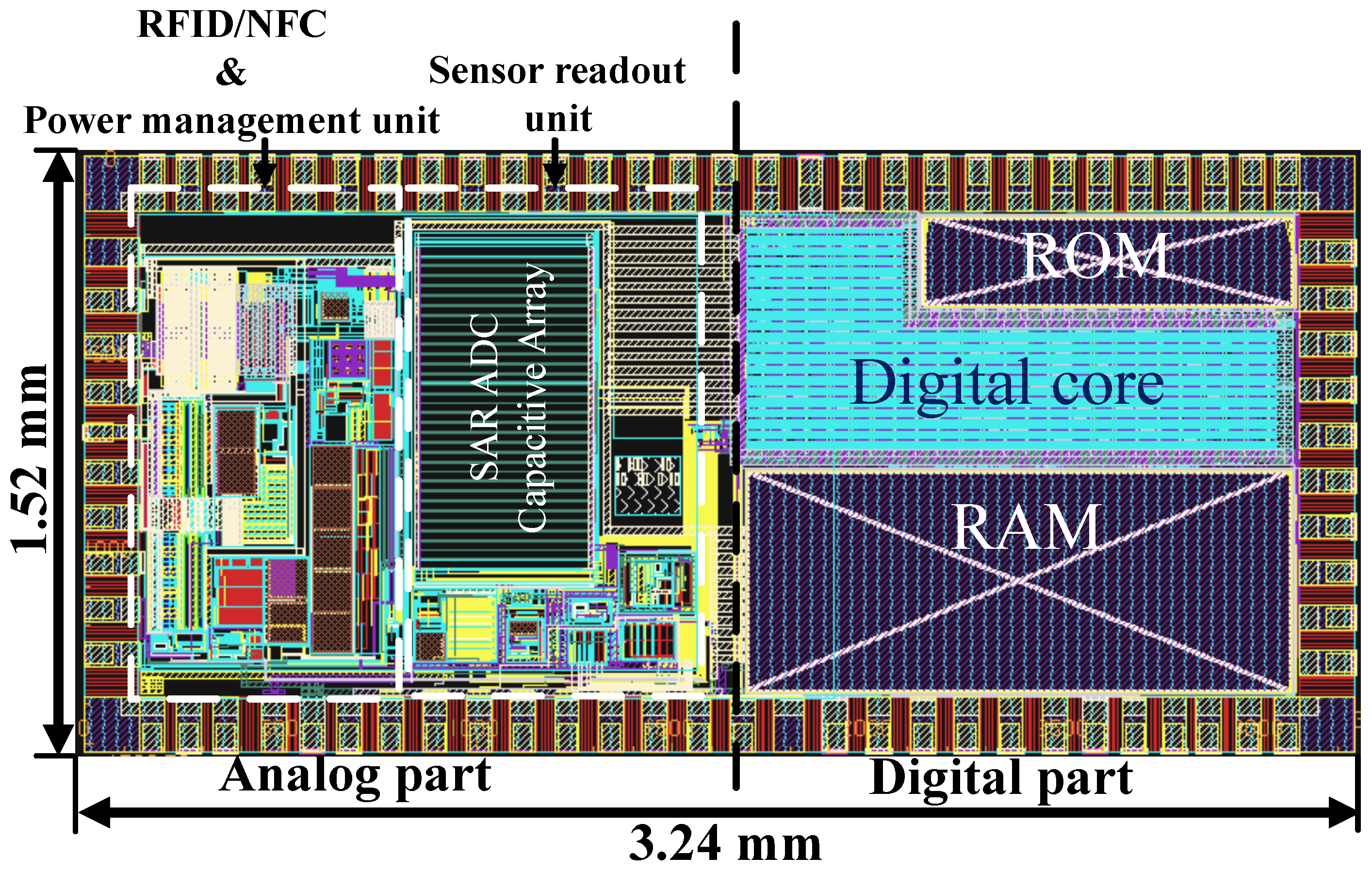
Low power, low cost inductively powered passive biotelemetry system involving fully customized RFID/NFC interface base SoC has gained popularity in the last decades. However, most of the SoCs developed are application specific and lacks either on-chip computational or sensor readout capability. In this paper, we present design details of a programmable passive SoC in compliance with ISO 15693/NFC5 standard for biomedical applications. The integrated system consists of a 32-bit microcontroller, a sensor readout circuit, a 12-bit SAR type ADC, 16 kB RAM, 16 kB ROM and other digital peripherals. The design is implemented in a 0.18 m CMOS technology and used a die area of 1.52 mm × 3.24 mm. The simulated maximum power consumption of the analog block is 592 W. The number of external components required by the SoC is limited to an external memory device, sensors, antenna and some passive components. The external memory device contains the application specific firmware. Based on the application, the firmware can be modified accordingly. The SoC design is suitable for medical implants to measure physiological parameters like temperature, pressure or ECG. As an application example, the authors have proposed a bioimplant to measure arterial blood pressure for patients suffering from Peripheral Artery Disease (PAD).
1. Introduction
Inductive powered biomedical systems brought in complete new dimension in the medical field over the last century. A bioimplant to consider excitable regions in the nervous systems is presented in [1], where the experimental study was conducted on Rhesus monkeys as early as 1949. A similar discussion is also done in the paper [2]. The work [3] demonstrates a pressure sensitive radio transmitting capsule for the study of motility in the gastrointestinal environment as early as 1957.
From the 1950s and 60s onward, the RFID (radio frequency identification) technology is extensively utilized for the design of the remotely powered systems. Since it was first patented in 1973 [4], RFID technology became more and more popular over the succeeding decades. A considerable insight into the evolution track of RFID is mentioned in [5]. The typical operating frequency of RFID varies from a low frequency range , HF (high frequency) range of to ultra-high frequency range of 860–960 MHz and 2.45–5.8 GHz. Biotelemetry systems using RFID have persisted around for years where it is utilized for sensing and wireless identification [6,7,8].
From 2000 onward, along with the growth of RFID technology, a fresh band of communication protocols was introduced based on the existing RFID standards which is usually known as NFC or near field communication. Unlike RFID, it merely goes on one band of a frequency of 13.56 MHz as it is only functional over a maximum length of 4 centimeters. The telemetry applications have been revolutionized by the introduction of NFC, as a handheld smart device can be utilized to interact. There are five different kinds of available standards for NFC which are type1&2-ISO/IEC 14443 A, type 3-JIS X 6319-4 (Felica), type4-ISO/IEC 14443 A/B and type5-ISO/IEC 15693 (18000-3). The proposed SoC (system-on-chip) is developed based on ISO 15693 standard which corresponds to the standard type 5 or simply NFC 5.
The first SoC appeared in an electronic watch in 1974 [9]. Since then, along with the advancement of silicon technology, SoCs had become an integral lot of electronic devices used in our day to day life. Our smartphones, tablets, laptops or artificial intelligence gadgets, all of them have dedicated SoCs. Complex circuitries can be included in a more limited area which includes analog circuits and digital logic, including memory devices and integrated computational platforms. So biotelemetry is no exception as it requires modest size and lower power consumption.
Table 1 presents an overview of the state-of-the-art SoCs for bio-medical applications. The NFC and RFID enabled ICs [8,10,11] are specifically used for glucose measurement. The SoC presented in [12] is reconfigurable and provides a possibility to integrate a wide range of sensor types (temperature, glucose, pH value and protein concentration) but it does not have an NFC communication interface. A batteryless body sensor node is recorded in [13] is suitable for acquiring, processing and transmitting electrocardiogram (ECG), electromyogram (EMG) and EEG (EEG). This is the only SoC among all which includes an 8-bit microcontroller without NFC communication capability. Thus, a batteryless (passive) SoC which includes RFID/NFC interface, PMU (power management unit), sensor readout interface, integrated ADC (analog to digital converters), integrated microcontroller and is unspecific to a particular application lacks. Our study demonstrates a passive, programmable SoC which includes all these features which are hashed out in detail subsequently.

Table 1.
State-of-the-art SoCs for biomedical applications.
The mixed signal SoC presented in this paper is designed for low power passive sensor system applications first proposed in [17,18]. The key features included by the state-of-the-art SoC presented in this paper are:
- Battery-less system (completely passive)
- RFID (ISO-15693) /NFC (NFC5) communication interface
- Power management unit
- Sensor readout unit including 12-bit ADC
- 32-bit microcontroller
- RAM (Random Access Memory)
- ROM (Read Only Memory)
The sensor readout unit is capable to acquire ECG data using electrodes, resistive sensor measurements, such as pressure and temperature. Low power design techniques and architecture are used to reduce the overall power consumption. By using the firmware the SoC can be programmed according to the requirement of the application.
The analog part of the SoC is responsible for energy management, RF communication, and sensor data readout. A 32-bit microcontroller, internal RAM, and ROM along with other peripherals are included in the digital part of the design. A much larger circuit complexity is included in a smaller area which makes it low power and cost-effective design. The external components required are memory devices, such as flash or FRAM, sensors, antenna and some passive components. An NFC capable smart device like a smartphone or a tablet can be used to communicate with a sensor tag developed with the proposed SoC.
Organization of the Paper
An application example of the SoC is presented in Section 2. Section 3 discusses in detail the ultra-low power design techniques applied to the design. The system architecture and the design details of the SoC are elaborated in Section 4. In Section 5, the complete layout of the SoC is presented, whereas in Section 6 the functional verification of the SoC is illustrated. Lastly, Section 7 manifests the overall conclusion of the work.
2. SoC Application Example and Advantage of 13.56 MHz Frequency Range in Biomedical Applications
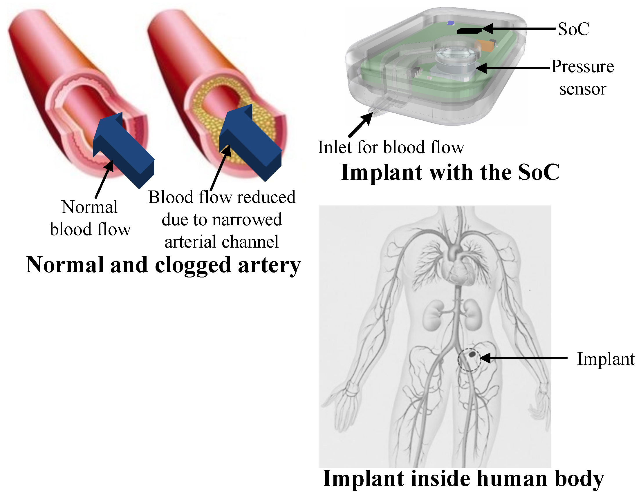
Although the intended application for the SoC is open and can be employed in industrial applications or as a medical implant to measure physiological parameters, such as temperature, ECG or blood pressure. One of the possible applications could be to develop a bioimplant to monitor blood pressure in the femoral arterial system for the patients suffering from Peripheral Artery Disease (PAD). Most of us are aware of arterial blockages in the heart or in the brain; a similar kind of blockage can also occur in places like arteries in the legs. PAD is commonly referred to the arterial blockage of the legs, but it can affect the other arteries (except heart and brain) too. A detailed discussion about the disease is done in the works [19,20]. The work [21] presents in detail the global distribution of the disease based on high-income and low-income countries. As per [21], in 2010 there were 202 million living with the disease, where it also asserts about the occurrence of the disease depending on sex and age of the individual. The idea of the proposed passive implant is to monitor the blood pressure within the blocked artery through invasive method. The particular individual can monitor the arterial condition by using his or her smart device. Figure 1 shows a simplified diagram of the implant realized by using the proposed SoC.
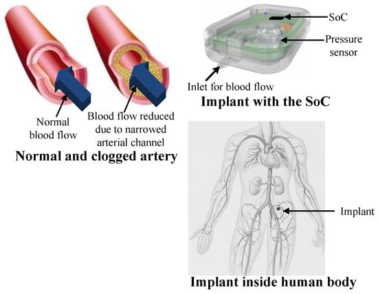
Figure 1.
PAD implant realized using the proposed SoC.
A bioimplant placed inside the human body operates in an environment consisting mostly of bone, skin, fat, blood and muscle. So there is a certain amount of energy loss as the dielectric constant of these body tissues are much greater than that of air. The relationship in between relative permittivity (), wavelength of the material () and that in free space () is given by the equation:
The value of depends on the frequency, Table 2 provides an overview of the value of and conductivity for different body tissues at the frequency range of , where = . The values are obtained from the Federal communications commissions (FCC) document where body tissue dielectric parameters are listed for 10 to 6000 MHz [22]. As the permittivity increases, the wavelength of the material decreases. The variation in the permittivity changes the direction of incident waves from one medium to the other (Snell’s law). However, this deviation is inversely proportional to the wavelength, at higher frequencies i.e., and above this deviation is much larger. The frequency range of provides a good tradeoff in-between wavelength deviation, read range and data rate.

Table 2.
Tissue dielectric parameters for 13.56 MHz [22].
3. Ultra Low Power Design Techniques
In modern-day electronics systems, low power design techniques are used to reduce the overall power consumption, of the system, whether it is a battery powered or a battery-less passive system. In this context, numerous methods are embraced by the designers to keep the power consumption as low as possible. A considerable insight into the ultra-low power circuit design is provided in the work [23], which explains the design details at the architectural, physical and system levels. The work presented in [24] illustrates “The Low-Power Hand” which is fundamentally a tradeoff in between precision, speed, topology, technology, and task for an energy efficient low power design. The work presented in [25] yields a thorough insight of the main design tradeoffs in between the supply voltage, delay, robustness due to technology scaling and variability. Low power designs in the context of wearable and implantable devices are discussed in [26].
3.1. Digital Power Consumption
First, we take a look into the digital power consumption; it can be observed that it is a sum of standby power or the leakage power , short circuit power and dynamic power consumption as given by the equation:
where is the power supply, is the leakage current, is the equivalent short circuit capacitance, is the capacitive load for the digital circuit, is the system clock frequency and (where ) indicates activity factor which is a function of circuit topology and activity of input signals. From Equation (2), it can be concluded that the power consumption of the digital circuits can be reduced if the supply voltage, clock frequency and the capacitive load are kept at bare minimum. A deeper insight into the same is provided in [23,24,26]. For the SoC, a system clock of is used, generated by the internal clock regenerator circuit. Slower clock and absence of an external clock source helps to keep the power consumption low. No wake-up unit manager is provided for the digital part as it is a battery-less system.
3.2. Analog Power Consumption
To reduce the power consumption of the analog circuits, weak inversion or sub-threshold region of operation is used [23,24]. The current equation for the device operating in sub-threshold region can be given as:
where is the technology dependent sub-threshold current obtained for = , where is the gate-source voltage and is the threshold voltage, is the thermal voltage, W/L is the aspect ratio and n is the sub-threshold factor [27]. For = , equation 3 can be further simplified as:
If W/L and are kept constant, only depends exponentially on , resulting in a much smaller current in compare to the saturation or strong inversion region. A vivid description about sub-threshold operation is provided in [27,28,29]. For the design of the analog part, weak-inversion region of operation is used extensively which is discussed in detail for some of the circuits.
Multiple supply voltages (VDD) can be used to reduce the overall power consumption. Some of the analog circuits are driven by the supply rail VDDI = 1.2 V and digital block, as well as the rest of the external circuits required for the design, are driven by the supply rail VDDE = 1.4 V to 1.8 V. All the analog signals interfacing with the digital block are level shifted to the voltage level of VDDE.
The parts of the analog block, which are unrequired to be always active, are kept switched off and are only activated whenever required for sensor data reading. This helps to reduce the overall power consumption to a great extent. The low threshold voltage transistor is another means to cut the overall power consumption, which is employed in some of the analog circuits.
4. System Architecture and Design Details of the SoC
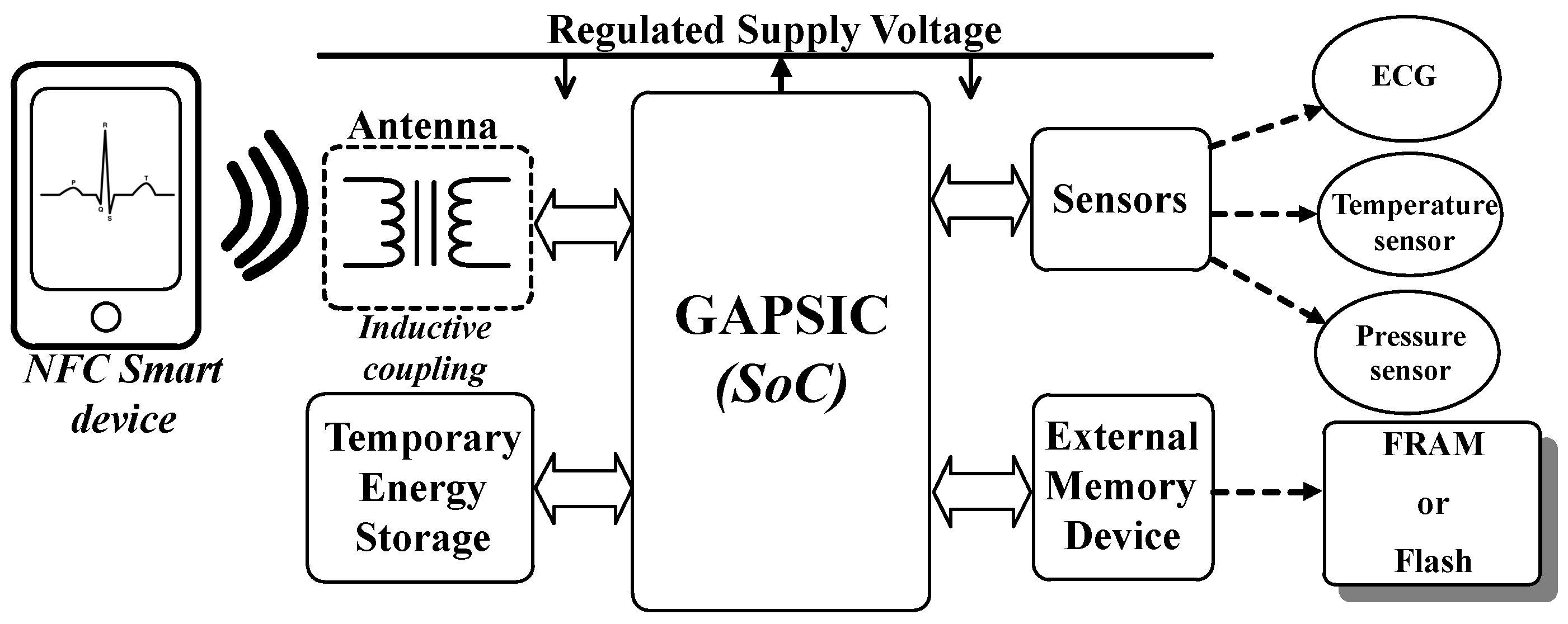
A simplified system overview is shown in Figure 2 for the passive tag system developed with the SoC. The reader device is an NFC capable smart device, but it can also be a standard RFID reader conforming to the ISO 15693 standard. The antenna shown is responsible for RFID/NFC communication as well as receiving energy from the reader device via inductive coupling. The energy available from the reader field is stored for a very limited period of time, by using a temporary storage device, such as a ceramic or a tantalum capacitor. The external memory device in the form of Flash or FRAM contains the application specific firmware. This makes an enormous flexibility in conditions of usability, as the SoC can be configured and the application program can be altered as per the demand. This is why the SoC is referred as GAPSIC which stands for General Application Passive Sensor Integrated Circuit.
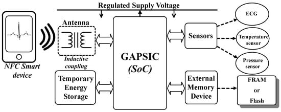
Figure 2.
System overview of a passive tag developed using GAPSIC-SoC along with some external components.
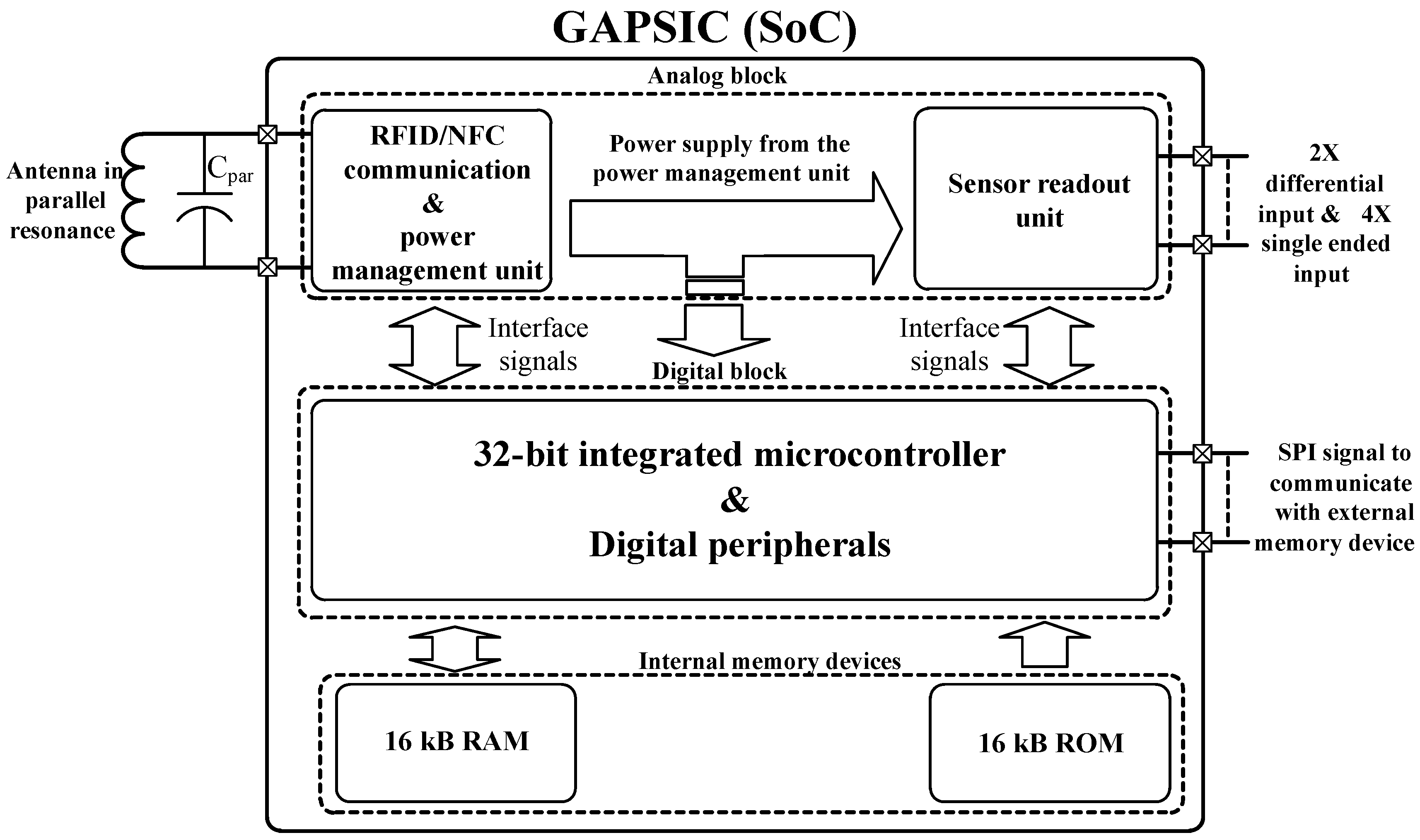
Figure 3 exhibits the internal architecture of the SoC, which consists of analog block, digital block, and internal memory devices. The analog block can be further split into two categories RFID/NFC communication and power management unit and sensor readout unit. The digital block consists of a 32-bit integrated microcontroller and digital peripherals. The internal memory devices include 16 KB RAM and 16 KB ROM.
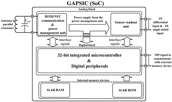
Figure 3.
Simplified system architecture of the proposed SoC-GAPSIC.
4.1. RFID/NFC Communication and Power Management Unit
This block is responsible for RFID/NFC communication and also for handling the entire power supply of the chip. Based on the functionalities, this block can be categorized into four different units, such as a power supply management unit, RF communication unit, field detector unit and clock regenerator unit.
In this section, only a brief overview is given, where some of the circuits are discussed in detail. This part is realized as a stand-alone chip which is tested for all of its functionalities. Figure 4 shows the system level block diagram of the RFID/NFC communication and the power management unit where all four functional blocks are shown.
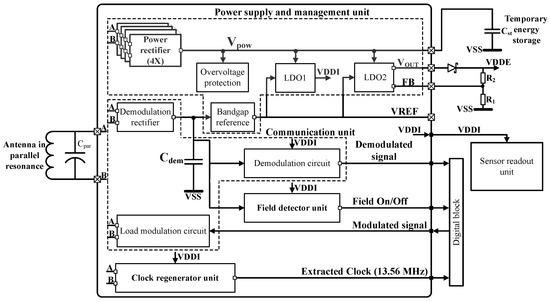
Figure 4.
System level architecture for RFID/NFC communication and power management unit.
4.1.1. Power Supply Management Unit
The power supply management part consists of over-voltage protection circuit, power rectifiers, bandgap reference and LDOs (low drop out regulators).
Over-Voltage Protection Circuit
The over-voltage protection circuit and the ESD (Electro Static Discharge) diodes protect the chip from over-voltage conditions. The over-voltage protection circuit consists of a bleeder circuit as discussed in detail in the works [30,31,32,33]. The maximum allowed limit for the over-voltage protection circuit is set by the technology which is .
4.1.2. Power Rectifier Unit
Figure 5 shows the power rectifier circuit which supplies both the LDO regulators to fulfill the entire energy requirement of the microchip. Some of the state-of-the-art power rectifiers are presented in recent times are presented in the works [34,35,36]. In this case, four gates, cross-connected NMOS passive rectifier is used in parallel. The working of a gate, cross-coupled NMOS rectifier is in detail discussed in [33], hence further explanation is avoided here. The phase inverse antenna inputs (A and B) switch on even and odd-numbered transistors in respective clock cycles. The power rectifier can support a maximum load of and has a maximum power conversion efficiency of 45% for a load of and an input power of .

Figure 5.
Circuit schematic of the NMOS cross coupled rectifier.
Bandgap Reference
The bandgap reference circuit is used to generate a temperature and supply independent reference voltage which is further used by the LDOs. The basic working principle of the bandgap reference circuit is provided in [37,38,39,40,41]. The work presented in [42] discusses about a bandgap reference circuit for RFID applications similar to the one presented here. The bandgap circuit is powered by the rectified voltage provided by the demodulation rectifier as shown in Figure 4. The average value of for nominal temperature of 25 °C. The minimum value of required to turn on the circuit is . The supply voltage sensitivity is at 25 °C for = to and has a start-up time of .
Low Drop out Regulators—LDO1 and LDO2
Two LDOs provide the regulated power supply for the SoC including all the external components. LDO1 provides a fixed supply voltage VDDI of for the internal analog blocks. LDO2 provides the supply voltage in the range of to for all the external components and the internal digital block. The output voltage of LDO2 can be fixed by choosing the resistors and as shown in Figure 4. Only LDO1 is discussed here as both the LDOs are similar. The LDOs presented in the works [43,44,45,46] analyzes the LDO fundamentals including different kinds of implementation. The LDO1 presented here is very similar to the one presented in the work [46] and is initially proposed in [47].
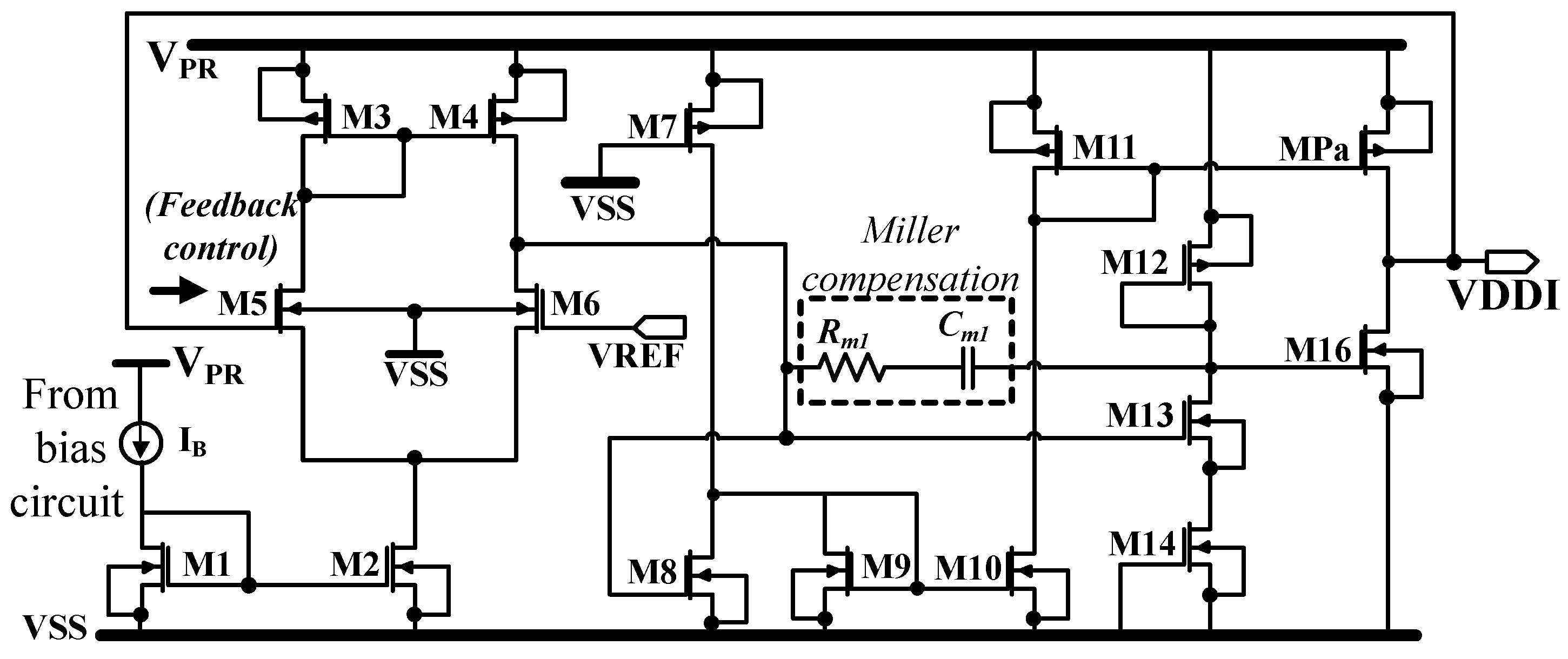
Figure 6 shows the schematic of the LDO1, where M3-6 forms the first stage, M7-11 forms the second (inverting) stage and the pass element MPa is the third stage. The devices M12-14 form a common source stage with source degeneration. This provides the gate voltage for the load device M16, which acts as an active resistor to set the output voltage at . To achieve a good phase margin and stability, a pole splitting capacitor in the form of Miller compensation is provided along with a resistor . Including only would have caused a right half plane zero (RHP), resulting in a stability issue.
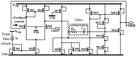
Figure 6.
Low dropout regulator 1 (LDO1).
The transconductance, output capacitance and the output resistance for each of the stages are denoted as , and respectively, where the subscript x indicates the respective number of the stage. The transfer function for the proposed LDO1, which is also the loop gain frequency response, is given as , which is further expressed by the following equation:
where is the output and the is the input voltage, k indicates the DC gain, is the zero and , , are number of poles for each stage. LDO1 never operates in a no load condition and has to support a minimum load of the communication unit, field detector unit and the clock regenerator unit and the maximum load is for the sensor readout unit. The transfer function is given for the maximum load condition, where the ≫ and . The for LDO1 is given as:
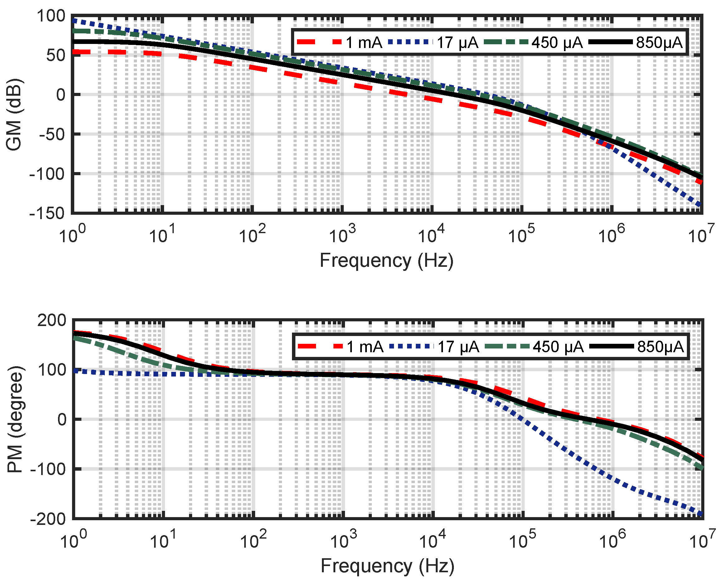
where A = and B = . For a large load current will be large and hence the pole has no effect on the stability. However, a minimum value of is required to maintain for stability reason in case of a smaller load current which is obtained from the loop gain simulation as shown in Figure 7. The differential pair of the first stage is kept in weak inversion region, second and third stage are kept in saturation. Some of the important design parameters are = , = and = , = and = . M12-14 are kept in cut off region, which drives the device M16 having an equivalent resistance of . The pass transistor MPa is designed with a channel resistance of and gate-drain capacitance of .
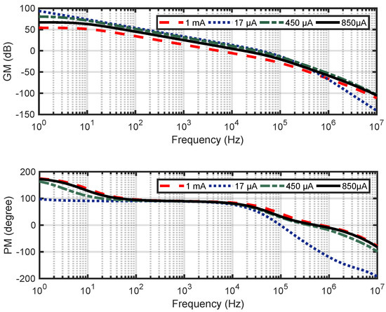
Figure 7.
Loop gain simulation. GM = Gain Margin; PM = Phase Margin.
The minimum and maximum load that the LDO1 needs to support ranges in between and respectively, however it is designed to support a maximum load of . The line regulation for minimum and maximum load is and respectively. It has a minimum load regulation of for a = and for a = . For the temperature range of −30 °C to 85 °C and a maximum load of it has a dropout voltage of . For a = , it consumes a power of . An output capacitor of is sufficient to provide stability for all possible load conditions i.e., from to . The average PSR (power supply rejection) is for all possible load conditions. Table 3 shows the stability analysis for different load conditions.

Table 3.
Loop gain parameters for different load conditions for = and at nominal temperature condition of 27 °C.
4.1.3. RF Communication Unit
The demodulator circuit consists of an envelope detector circuit, first order high pass filter, and a comparator. The demodulation rectifier used is a passive rectifier similar to the one implemented for the power rectifier, but with much smaller device dimension as it needs to support a maximum load of . The envelope detector circuit is used to extract the message sent by the reader, which is further given to the comparator circuit to generate the digital bit sequence. The rectifier provides the DC level of the envelope signal, the capacitor stores the charge for a short period of time, which is then discharged through the resistive load which is the bandgap reference circuit itself. The current consumption of the bandgap reference circuit is used as the current load for the envelope detector circuit. For , a capacitor is used where the average minimum and maximum discharge time is and respectively.
4.1.4. Field Detector Unit
A digital Schmitt trigger circuit is applied to detect the RF field, similar to the one explained in [48]. When the field is detected, the output goes high or else it is low. The low pass filter has a cutoff frequency of as it prevents the Schmitt trigger to alter its state instantaneously in case the RF field is on or off for a very brief period of time. The field on/off signal is further used as the system reset signal by the digital block. The switching on and off time for the circuit is and respectively.
4.1.5. Clock Regenerator Unit
The clock regenerator unit extracts the clock from the RF field. An RS (set-reset) logic latch is used which is implemented using two NAND gates. The extracted clock pulse has a frequency of and a duty cycle of 50 ± . This clock is further divided by half () to be used as the system clock. All other clocks required by the SoC are further generated from this clock and no external clock source is used.
4.2. Sensor Readout Unit
The sensor readout unit is initially proposed in [47,49], which is further modified. Figure 8 shows the system architecture of the sensor readout unit proposed here, which consists of channel selector, virtual ground generator, PGA (programmable gain amplifier) and a 12-bit SAR (successive approximation register) type ADC (analog to digital converter). In the following sections, the design of some of the circuits is discussed in details.

Figure 8.
System level architecture for sensor readout unit.
4.2.1. Channel Selector, Bias Generator Circuit and Virtual Ground Generator
The channel selector is realized as a multiplexer which is programmable and can be selected by the digital block. It has two differential and four single-ended inputs.
The bias generator is responsible for generating the bias voltages = , = and = at nominal (27 °C) conditions.
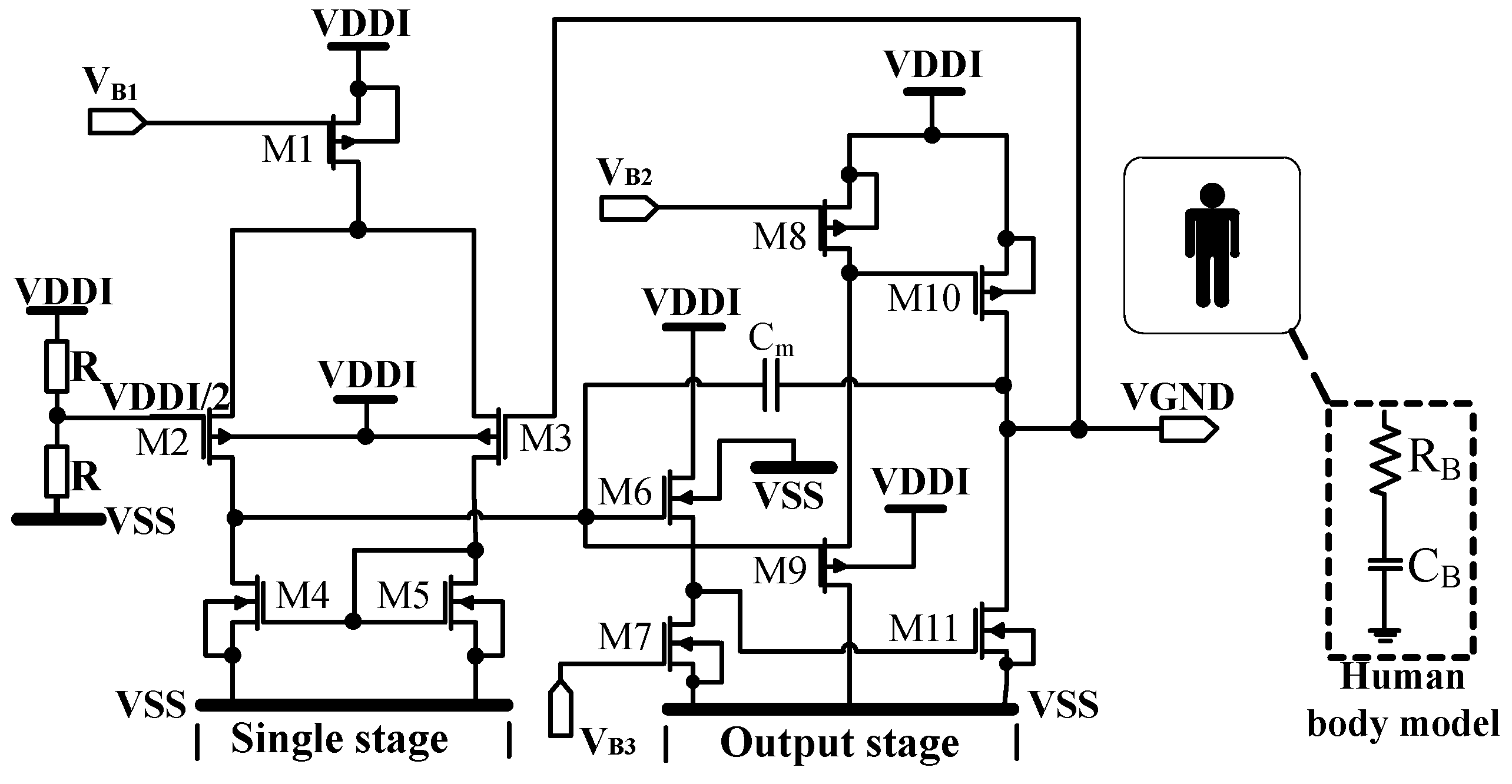
The virtual ground generator fulfills two purposes. Firstly, it provides the reference voltage VGND for the channel selector, PGA and the comparator for the SAR ADC. Secondly, as it is compatible with the human body model, it can be used as the reference potential by the reference electrode for the ECG measurement. Figure 9 shows the simplified circuit diagram of the virtual ground amplifier circuit which is a voltage follower circuit configuration. In the figure, the human body model is characterized by a resistive load = and a capacitive load = , which forms a low pass filter. The output stage of the virtual ground generator shall be able to source and sink current. For this, a PMOS differential amplifier is used as the first stage, which is followed by two common source amplifier stages CS1 and CS2 consisting of PMOS (M6) and NMOS (M9) devices respectively. Both the CS stages provide the voltage headroom close to both the rails for the class AB output stage. Class AB amplifier is ideal to drive larger load capacitances as the push-pull output stage can both sink and source current. M2, M3, M10, and M11 are kept in saturation, M6 and M9 are in weak inversion region. The transconductance () for each of the stages is given as follows: = , for CS1: = and for CS2: = .

Figure 9.
Input buffer amplifier used to generate virtual ground potential VGND.
With a decoupling capacitor of , it has a slewing time of , settling time of and an error band of for a temperature of 37 °C which is the normal human body temperature. The closed-loop bandwidth at 37 °C is and has a closed-loop output resistance of . At no load condition, VGND = and has a load regulation of . It has a total power consumption of and a minimum and maximum settling time of (at 85 °C) and (at −30 °C) respectively depending on the temperature. For this design, low threshold voltage transistors are used to keep the overall power consumption, low in comparison to the high threshold voltage transistors.
4.2.2. Programmable Gain Amplifier—PGA
The PGA is implemented using a three op-amp IA (instrumentation amplifier). There are different topologies which can be used to implement an IA some of which are presented in the works [50,51,52]. In this topology, no offset cancellation technique is provided rather the offset voltage is measured prior to every measurement, which is stored digitally. The stored offset value is then canceled from the measured sensor data.
Figure 10, shows the schematic diagram of the IA used here, where the input stage op amps and act as the voltage follower for the inputs and . The input resistance of the op amps and is desired to be as large as possible (ideally infinite) so that the signal to be measured remains undistorted. The input stage amplifies the differential signal but allows the common mode signal to pass through without any amplification.
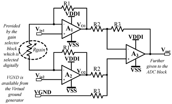
Figure 10.
Programmable gain amplifier configuration used where = = = R = .
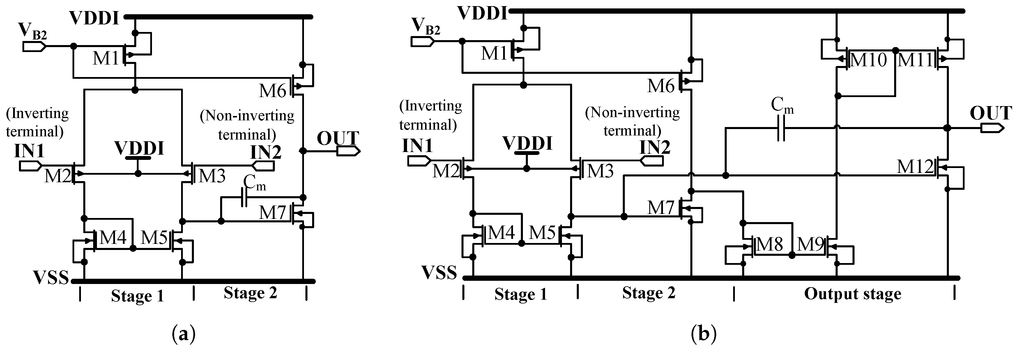
Figure 11 shows the input stage op-amp and used, which are identical for the design. A two-stage amplifier is used for this purpose with a small compensating capacitor . It has a loop gain of and an offset voltage ranging from (−30 °C ) to (+85 °C ), having an offset drift due to temperature by . It has a closed loop trans-impedance of and a closed loop gain of in the frequency range of . It provides a CMR of at unity gain configuration and has a power consumption of .
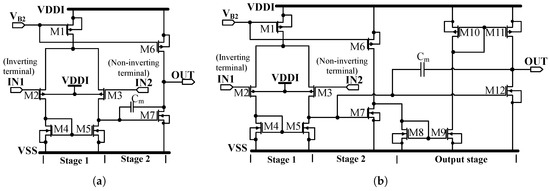
Figure 11.
(a) Input buffer stage (A1 and A2) operational amplifier for the IA; (b) Difference amplifier used for the IA.
The difference amplifier is a three-stage amplifier, where first stage amplification is provided by the M2-5, M7 and M6 provide the second stage amplification and the current buffer M8-12 provides the third stage amplification. The topology is very similar to the one used for the LDO1 (Section 4.1.2) hence further explanation is avoided. The difference amplifier has an offset value ranging from to depending on temperature and process variations and has a value of at nominal conditions (27 °C).
The resistor as shown in Figure 10, is used to adjust the overall gain of the PGA, which is selected digitally by using the gain selector. The amplification of the PGA can be adjusted from 1×, 2×, 10×, 20×, 40×, 50×, 80× and 100×. The op-amp is arranged in the difference amplifier configuration involving the resistors and .
The output of the difference amplifier is given as:
where and are the inputs and the G is the gain which is given as:
In this case = = = R = . Hence the gain factor G can be given as:
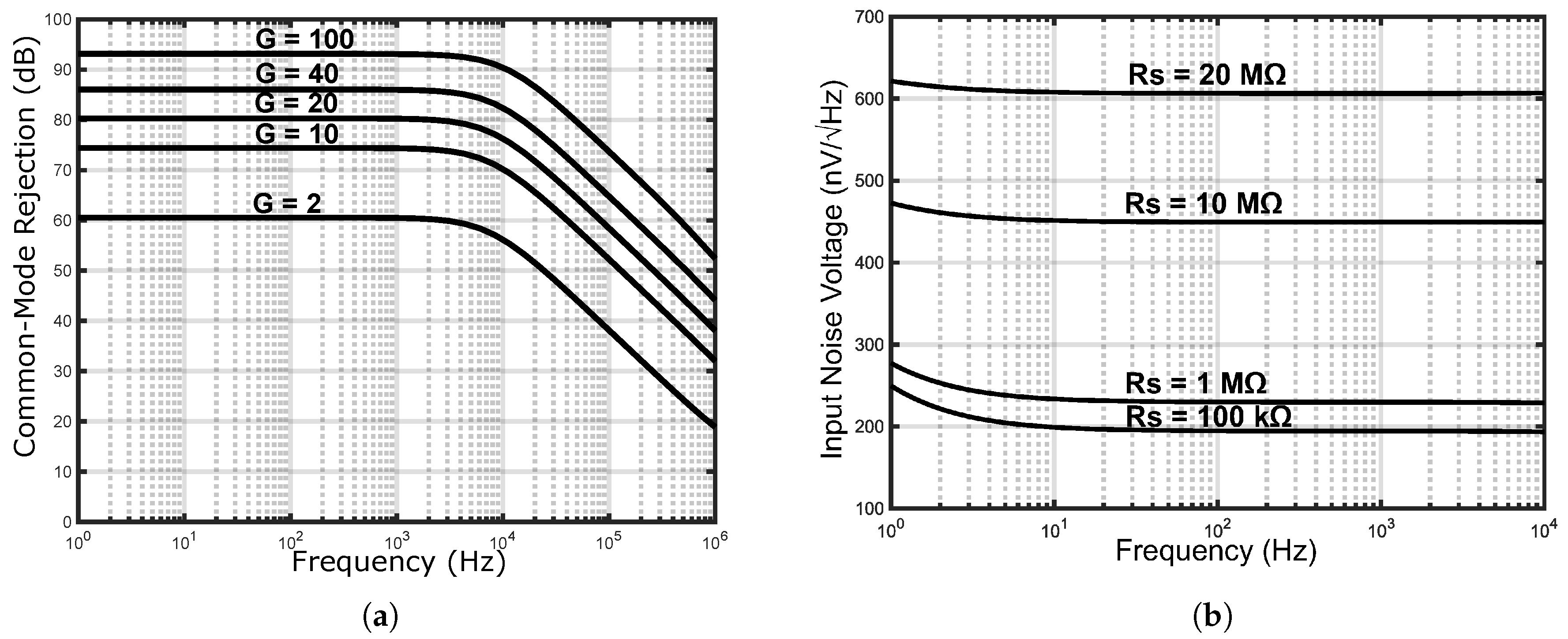
The common mode signal is removed by the difference amplifier stage. CMR (Common mode rejection) provides an idea about how the PGA will behave in the presence of common mode input voltage. The CMR of the difference amplifier largely depends on the matching of the and resistors which are of the same value and in layout inter digitization is used for better matching. Figure 12 shows the CMR for different gain factor over the frequency range. For a gain of 100×, PGA has a CMR above , which is a good figure-of-merit. In case of physiological signal measurement like ECG, the source impedance is in megohm range. Figure 12 yields an estimate of the effect of source resistance on the input noise figure in the measurement process which ignores the noise contribution of the source itself. For better noise immunity, a guard ring is provided in the layout around all the structures of the PGA. The differential pair of is realized by using common centroid layout to avoid variation due to temperature and process gradient. As obtained from the simulation for the PGA, for unity gain configuration, the closed loop output impedance is , a CMR of and a power consumption of . For a load resistance of and a load capacitance of , the average SR (slew rate) of the PGA varies in between to . The input impedance is at while the closed loop output impedance varies from to for gain 1× and 100× respectively. The gain margin is for a load capacitance of and the 3 dB roll-off frequency is at .
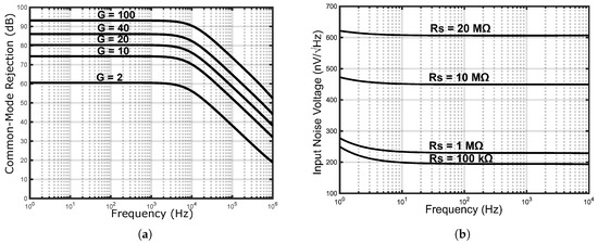
Figure 12.
(a) Simulated CMR (Common mode rejection) for the PGA; (b) Simulated input referred noise of the PGA for different input source resistances.
4.2.3. SAR (Successive approximation register) type ADC (analog to digital converter)
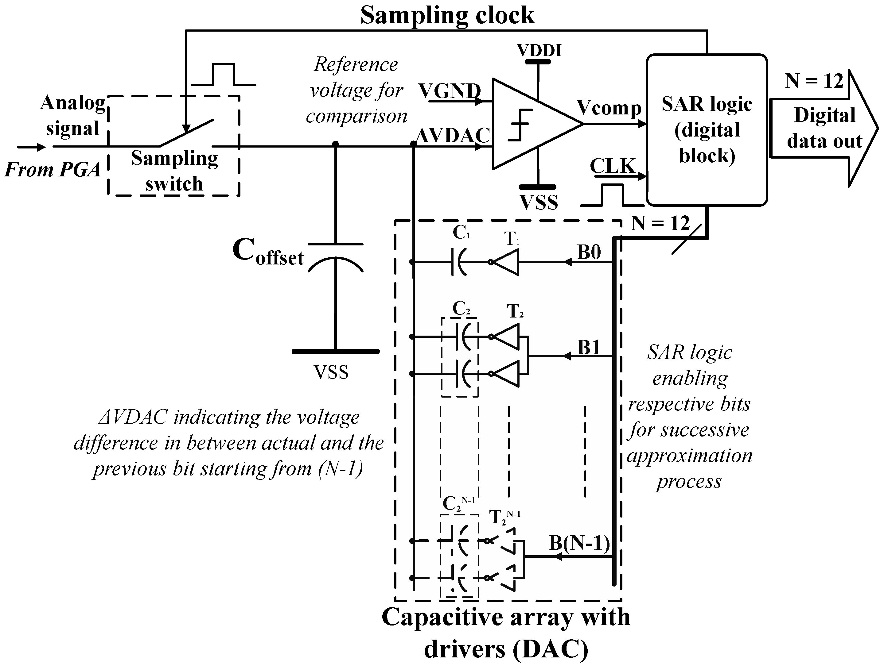
A comparative study of different SAR architectures based on power consumption and linearity is provided in [53]. A 10-bit SAR ADC for medical implant devices with a novel switching scheme to improve the energy efficiency is presented in [54]. Some other state-of-the-art designs presented in recent times are [55,56]. The SAR ADC discussed here is based on the architecture provided in the work [57] which is again based on the work [58]. The basic architecture of the proposed SAR ADC is shown in Figure 13. The ADC module strictly comprises of a sample switch, comparator, capacitive array and SAR logic implemented in the digital block. In this architecture, the power consumption is less as each bit gets selected by the SAR logic, which is further added to the sampled input, which is the principal difference between this scheme and the conventional SAR ADC. For each addition of the input signal, the ΔVDAC is compared by the comparator with the reference voltage VGND, in case it is greater than the reference, the comparator gives a digital output of ‘1’ else ‘0’.
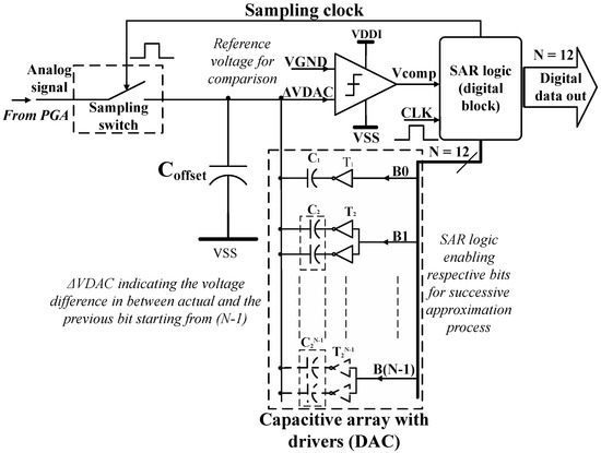
Figure 13.
Schematic diagram of the 12-bit SAR ADC.
Sample and Hold Circuit
The process of sampling is controlled by the SAR logic module which is part of the digital block and depends on the mode selected for the ADC conversion. In case the only single conversion mode is selected, it is activated by using an active low signal and again deactivated after single conversion is over, but in case of continuous conversion mode, the process continues till it is stopped explicitly. The sampling switch is accomplished by using a transmission gate. In general, for each of the components used in the signal path, the input capacitance and the effective channel resistance shall be kept as low as possible. The transistors used in the transmission gate are divided into equal numbered fingers. This diminishes the effect of the gate capacitances in the input signal value.
is the equivalent resistance of the sample switch and is the equivalent load capacitance for the sampling switch. The time constant for the DAC (digital to analog converter) circuit can be given as:
The relationship in between sampling time and is given as:
The designed maximum value of is and that of is ∼18 pF, the value of obtained is which is much faster than the maximum which is with sampling frequency. The voltage spikes originating due to gate capacitances of the sampling switch, the comparator and the DAC circuit itself is damped out through the low resistive path provided by the output stage of the PGA which is able to sink current due to its low output impedance which is ± as obtained from the simulation.
ADC Comparator
Comparators are the key components for an ADC as it sets the accuracy in terms of resolution and the working range of the ADC. The ADCs use either continuous time comparators or latch comparators. Most of the designs incorporate the latch comparator as it is less sensitive to noise distortion in comparison to the continuous time comparators as presented in the works [58,59,60,61,62,63,64,65]. This is due to the separation of the input and output stages but they have a discrete time operation. The work [66], presents a mathematical model for using multiple comparators to reduce the overall power consumption of the SAR ADC.
In this case, a low noise, low offset open loop comparator is used for sensing the voltage difference between each byte and the reference voltage VGND. The input capacitance plays an important role as it adds up to the stray capacitance affecting the overall accuracy of the capacitive array of the ADC.
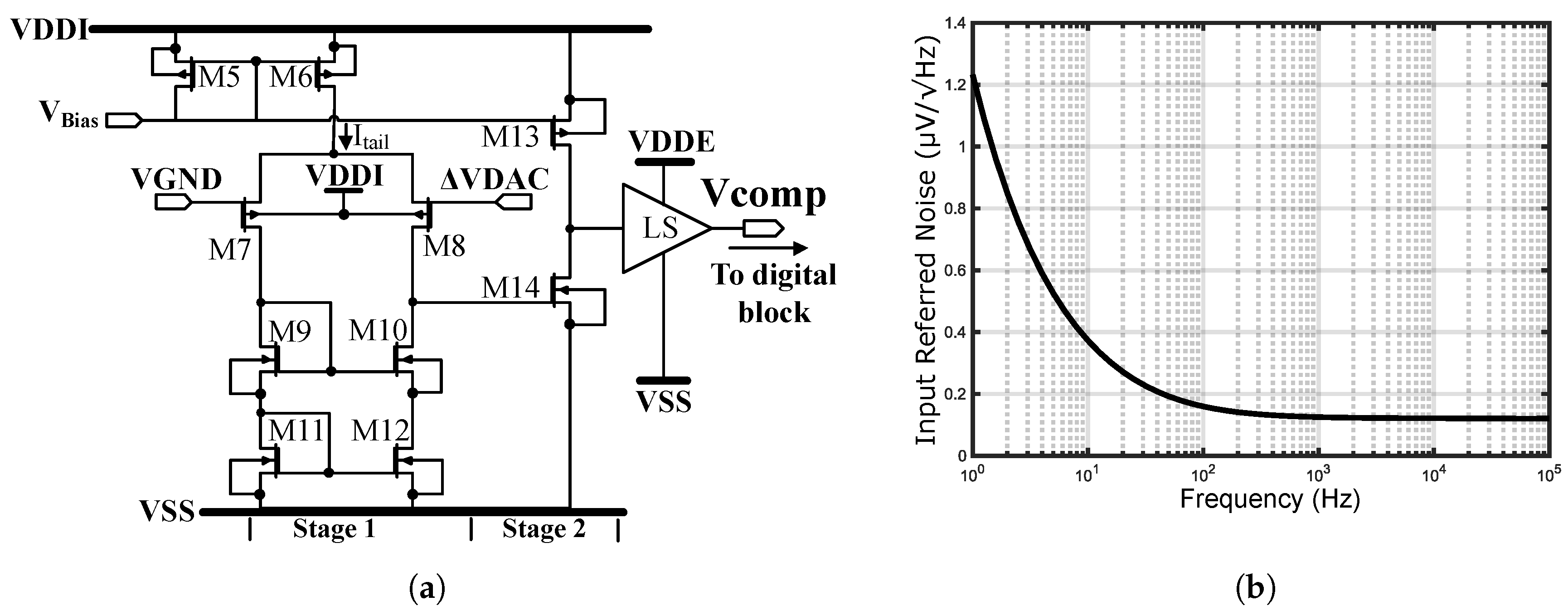
The practical realization of the comparator is shown in Figure 14, where a two-stage operational amplifier is used. The first stage is realized by using a PMOS differential pair M7-8 with cascode load comprising of M9-12. The sensitivity of the comparator largely depends on the gain of the differential pair which in turn depends on the transconductance and the output resistance. As the output resistance of the ’Stage 1’ is increased due to cascoding, the differential stage has an increased gain at the expense of limited output voltage swing. This is again compensated by ’Stage 2’ which provides the voltage swing. Higher loop gain ensures good CMR value and lower input offset voltage. In order to have higher transconductance values for the input differential pairs, wide channel transistors are chosen in parallel in order to reduce the gate resistance. Multiple fingers are used to design each of the transistors as it reduces the effect of the input gate capacitances. The use of fingers can only minimize the effect of the gate capacitance mostly the gate-source capacitance but cannot eliminate it completely. The input voltage difference will result in large voltage spikes due to voltage transition caused by the input capacitances. The gate-drain capacitance will generate this spikes/edges to be translated back to both the input nodes. So a lower input capacitance is necessary, along with it the output stage of the PGA and the sample switch shall be able to sink sufficient amount of current in order to reduce the time constant required to discharge the capacitances. The designed input gate capacitance of the differential pair is , gate-drain capacitance is , drain junction capacitance is and source junction capacitance is .
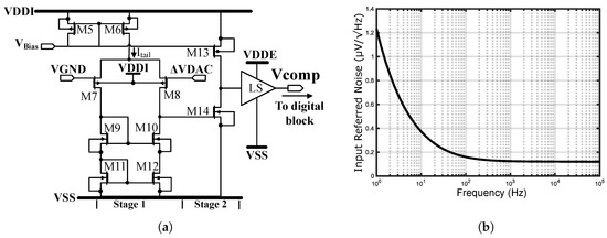
Figure 14.
(a) Schematic of the open loop comparator used for the ADC where LS indicates level shifter; (b) Simulated input referred noise of the ADC comparator for a source resistance of and input capacitance of .
Along with the input offset voltage, the thermal noise and the noise also brings in limitations for the accuracy of the comparator. The total input referred noise figure for the comparator is illustrated in the following noise analysis part.
The gain provided by the first stage of the comparator is and that of second stage is , where the overall gain is given by:
where is the gain for the first stage and is the equivalent output resistance for the first stage. Now = = and is given by the equation:
Equation (13) can be further interpreted as Equation (17) in terms of transconductance and output resistance for the individual devices where suffix i denotes the respective device from Figure 14.
The total input referred noise is given as the sum of low frequency noise or noise and thermal noise. For the noise analysis, the noise contribution for each of the stages are considered depending on the region of operation for the individual devices.
Since the noise sources are uncorrelated, the principle of superposition can be used for the addition of the noise power. The noise for the first stage differential pair is given as:
where is a process dependent constant for PMOS devices provided by the foundry, is the oxide thickness, is the device dimension for M7-8 and f is the frequency. The process dependent factor is smaller for PMOS devices in compare to the NMOS devices () as the later uses buried channel to carry holes. The thermal noise depends on the region of operation. Similarly the low frequency noise contribution for the second stage is given by:
As shown in Equation (19), if the process dependent factors are kept constant, the noise is only dependent on the device dimensions. Hence large device dimensions are chosen to ensure smaller noise figures at low frequency.
and are the device dimension and transconductances for the devices M13 and M14 respectively. So the total noise for both the stages combined are given by:
For long channel devices operating in strong inversion region the noise current is given by:
where is called the excess noise factor. For devices in strong inversion = for long channel devices and ≥2 to 3 for short channel devices. For devices in weak inversion region = . The thermal noise voltage for individual devices is given as:
where is the output resistance for the particular device. For the first stage the differential pair (M7 and M8) and the load devices (M9-12) operate in weak inversion region. The total output thermal noise for the first stage is given as:
Similarly for the second stage the thermal noise figure can be obtained depending on the operating region for the individual devices. The device M13 operates in strong inversion region and M14 is kept in weak inversion region, so the second stage output thermal noise is given as:
Total input noise figure for the second stage is given as:
So the total input thermal noise contribution for the first stage and the second stage combined is given by the sum of Equations (25) and (28):
The total input noise figure including both the low frequency and the thermal noise is given as:
Due to cascoding of the load for the differential pair, has a smaller value in compare to the differential pair without cascoding load. The usage of cascode load and weak-inversion operation, reduces the overall input noise figure for the comparator. The input noise simulation for the comparator is shown in Figure 14, for an input source resistance of and an input capacitance of . From the figure, one can see noise figure is very low which is at frequency.
The SR is also dependent on the region of operation. The slew rate is given by:
where GBW is the gain bandwidth. Now for weak inversion region = , hence Equation (31) can be written as:
Hence, if the GBW is kept constant, the SR for weak inversion is only dependent on the temperature T.
The differential pair M7 and M8 is divided into four parallel transistors and each of them are arranged in a common centroid layout to avoid the effect of mismatches due to temperature or oxide gradients. The current mirrors and bias circuits are also constructed by using dummy transistors to reduce the effect of mismatches. The usage of the sub-threshold operation helps to reduce the offset voltage value and the overall power consumption. For typical cases at a nominal temperature (T = 27 °C), the comparator has a sensitivity of and for human body temperature (37 °C) the offset is at . Some of the key figure-of-merits for the comparator is listed in Table 4.

Table 4.
Important parameters of the comparator as obtained from the simulation.
ADC Capacitive array
The capacitor array for the ADC can be implemented in a different manner, for example, the works [64,67] have a split architecture with two separate DACs. The work [65] implements the DAC array with differential capacitor networks, which are composed of 10-bit split schemes along with an additional sampling capacitor. The work presented in [62] uses a segmented binary weighted capacitor DAC. In this case, a charge redistribution type DAC is used with a binary weighted capacitor array [58,59,61,65].
Physically the capacitor arrays are manufactured by using unit metal, i.e., two top metal layers in MIM (metal-dielectric-metal) capacitors which reduce the effect of fringe capacitances to a considerable extent. This because of capacitance, in general, is inversely proportional to the distance in between the parallel plates. Hence, considering the dielectric constants and the overall area are kept constant, the capacitance value will be reduced as the distance between the metal layers and the substrate increases.
In a conventional switching scheme of SAR ADC, a lot of energy gets lost in charging and discharging the capacitors as also mentioned in [57]. Also, the energy required to charge and discharge a capacitor is directly proportional to the value of the unit capacitor used. The value of the unit capacitor largely depends on the thermal noise and the mismatch where the later plays a dominant role. A detailed discussion regarding the nominal value of the unit capacitor and the standard deviation due to mismatch is provided in the works [61,68,69,70]. The matching of a MIM capacitor can be given as:
where is the standard deviation of the capacitor mismatch, is the matching coefficient and is the capacitor area. Further it can be simplified for the standard deviation for a single capacitor:
In the CMOS process used here, the MIM capacitor has a density of and a matching of 1%. Keeping this in consideration, the value of the unit capacitor chosen is with a dimension of × . A test structure for the characterization of small metal fringe capacitances is discussed in detail in [71]. An offset capacitor is included so as to set the entire voltage range of conversion which also depends on the accuracy of the comparator. Each of the bits is represented by a capacitor value starting from 2N to 2(N-1) where ‘N’ denotes the number of bits. For the LSB (least significant bit), the number of the unit capacitor is 1 and for the MSB (most significant bit) it is 4096. Each capacitor has a driver stage which is again controlled by the bit value. This reduces the effect of variation in line impedance [49] which in this case is same for each capacitor as shown in Figure 13. The total capacitance value is 16.36 pF and as the VDDI is 1.2V the range of ΔVDAC:
where the voltage range lies in between 1.06 V (max) and 150 mV (min). The equivalent digital value can be calculated by using the following relationship:
where is the value of the analog input signal, = , = and N = 1 to 12.
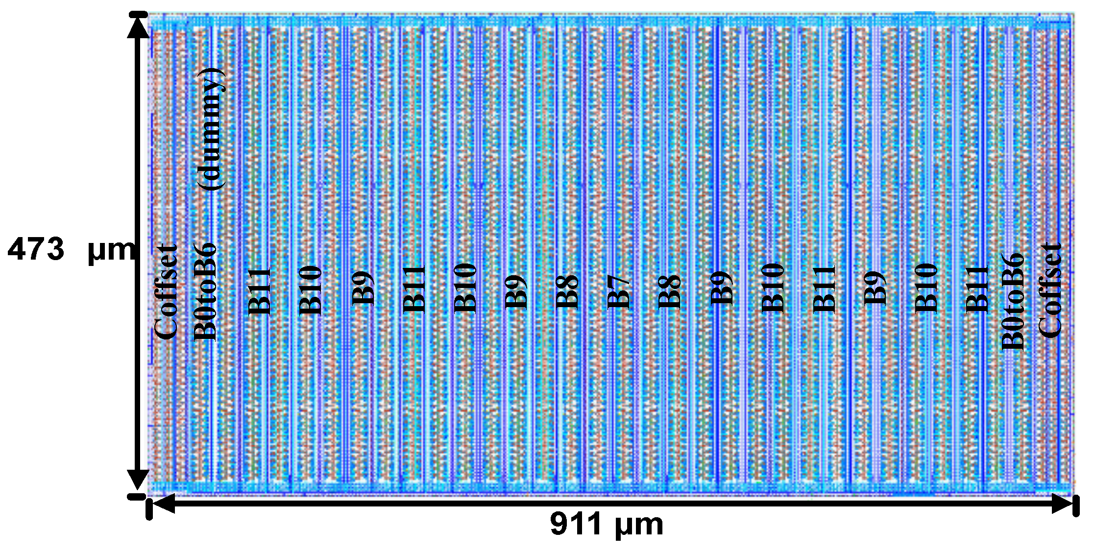
Only mismatch consideration for the unit capacitors is not enough; a common centroid layout is required for the capacitive array to avoid the consequence of the temperature or the process gradients. A considerable insight, into the DAC layout strategy for mismatches, is provided in [72]. Most of the designs use a full centroid layout, as in [57]. In this case, a partial centroid layout is used as shown in Figure 15 which is similar to the layout presented in [61]. The bit 0 to 6 and bit 7 are constructed without centroid layout, whereas bit 8 to bit 11 are constructed by using centroid layout. All the rows in the layout are constructed symmetrically including the offset capacitors by using the bit 7 as the unit cell. In this way, the total area for the capacitor array can be kept around 8.75% of the complete chip area. Dummy capacitors are provided to maintain the same environment for all the capacitors and the capacitor units are isolated from each other by using guard rings.

Figure 15.
Partial centroid layout of the ADC capacitive array.
Post layout simulation is done after parasitic extraction in order to realize the effect of the parasitics on the design. The complete input range of the ADC is , the theoretical value of LSB is which is smaller than the one proposed in [57]. The effective resolution of the comparator is without any mismatches, which is almost 28 times smaller than the LSB. The differential non linearity (DNL) and integral non linearity (INL) is simulated with a sinusoidal signal of peak-to-peak close to the Nyquist frequency () and the sampling rate used is . The simulated INL is +0.62/−0.56 LSB and simulated DNL is +0.5/−0.68 LSB.
From the knowledge of DNL the signal-to-noise-ratio due to quantization can be estimated by:
where N is the number of bits for the ADC and λ is the threshold value in the Gaussian probability function. For N = 12, λ = 3.0 and DNL = −0.68LSB, =. From this the effective number of bits (ENOB) can be calculated by using the formula:
which gives a value of =. The estimated value for Spurious-free-dynamic-range (SFDR) is which is obtained from the knowledge of INL by using the relation =.
4.3. Power Consumption Distribution of the Analog Part
The RFID/NFC communication and power management unit consumes . The sensor readout unit consumes which make a total power consumption of for the analog block. Figure 16 shows the power consumption, distribution for the analog block. In the power management unit, the majority of the power is consumed by LDO1 = , LDO2 = and bandgap reference circuit = . The communication circuit consumes , the field detector and the clock regenerator consumes and respectively. In the sensor readout unit, the most of the power is consumed by the PGA = and Virtual ground generator = . Other than that, the power consumption for the bias generator is and that of the ADC module which includes the comparator, DAC and sampling switch is .
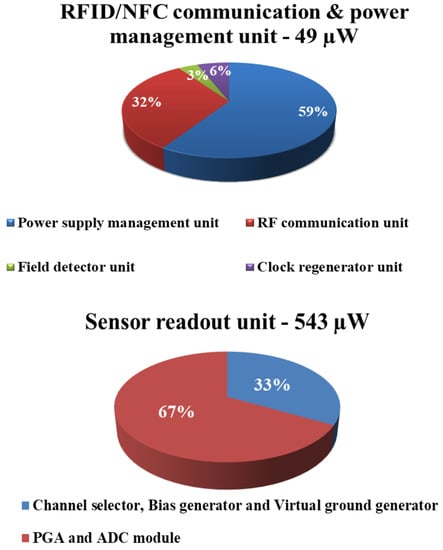
Figure 16.
Power consumption distribution of the analog block.
4.4. Digital Design
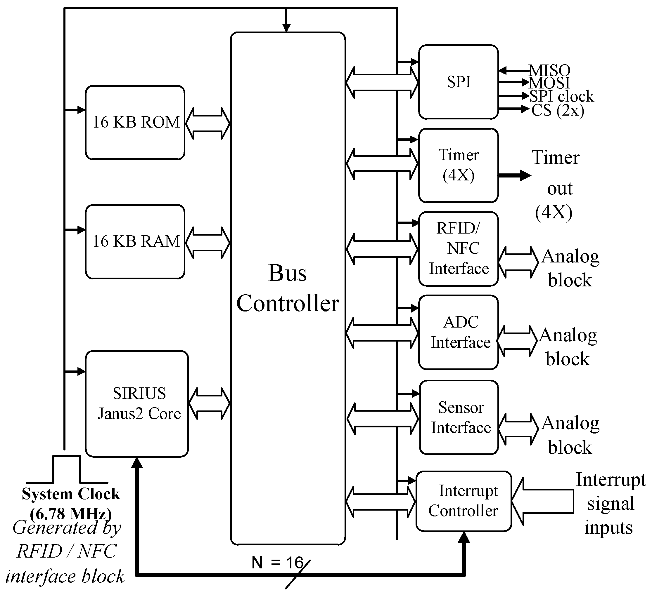
Figure 17 shows the digital architecture of the proposed SoC which consists of a 32-bit microcontroller core (SIRIUS JANUS 2.0), memory cells (RAM and ROM) and other peripherals. The field on/off signal generated by the field detector circuit is used as the reset for all the digital peripherals including the microcontroller.

Figure 17.
System level block diagram of the digital block for GAPSIC.
The microcontroller used here is developed by the ASIC design center at Hochschule Offenburg, based on the Von Neumann architecture proposed in [73,74]. Since then, further modifications have been carried out over the years, and the present version has been the one presented in [75]. It has a 16-bit data bus and a 32-bit address bus and the arithmetic and logical operations are based on Reduced Instruction Set Computing (RISC). The microcontroller is designed to operate at a frequency of , for this SoC it operates at a much lower frequency of . Slower clock frequency has two-fold advantages: firstly no internal PLL (Phase locked loop) is required which otherwise would have occupied 12.5% extra area; secondly, the slower clock frequency ensures that overall power consumption of the digital part remains low - which is already discussed in Section 3.
The SPI (serial peripheral interface) is used to communicate with the external memory device like a flash or a FRAM, where the application firmware is kept stored which is uploaded into the internal RAM of the SoC. The standard SPI signals used are MISO (Master input slave output), MOSI (Master output slave input), SPI clock and two CS (chip select) outputs. The maximum SPI clock frequency is of the system clock. One of the chip select is by default set for selecting the external memory device while the other chip select is free to be used for another SPI device.
There are four timers available, out of which two are dedicated to the internal operation and two are left free to be used by the application firmware if required. One of the internal timers is used by the bootup routine, and the other one is used by the RFID/NFC interface block.
The RFID/NFC interface consists of the digital logic required to extract the message from the demodulated signal and subsequently preparing the response.
The ADC interface consists of the SAR logic, ADC clock pre-scaler, data registers and control registers. The SAR logic consists of the binary logic required for the measurement in successive approximation. The SAR logic consists of shift registers which enable each bit starting from the MSB synchronized with the ADC clock. The ADC has a maximum conversion rate of and a sampling rate of ; further, it can either be operated in single or continuous conversion mode. At the end of a conversion cycle, an interrupt signal is generated. The interrupt signal is then synchronized with the system clock, to avoid the asynchronous operation. The result of the ADC conversion is stored in two eight bit data registers, one for MSB and the other one for LSB values.
The ROM contains the initial bootup process, which includes a hardware initialization routine required to make the SoC functional and an SPI routine. The SPI routine initiates the SPI communication in between the SoC and the external memory device, as it loads the application specific firmware from the external memory device into the internal RAM. The ROM also contains a UID (unique identification) for the SoC which can be read by using the RFID or NFC communication protocol. This is also part of the initialization check for the system, which assures the integrity of the hardware and the internal memory of the system.
4.5. Duty Cycle of Operation
Figure 18 shows a brief overview of the complete duty cycle of operation involved in a measurement process in case a single ADC conversion mode is activated. The boot-up sequence requires the maximum duty cycle, which is nearly 75%. The sensor readout unit which consumes the maximum power in the analog part is only active for approximately 5% of the entire duty cycle.

Figure 18.
Brief overview of the timing sequence and hence the duty cycle for different events involved in a measurement process, considering only single ADC conversion mode is activated. Note: Config.—Configuration; comm.—communication; meas.—measurement.
5. Complete Layout of the SoC
Figure 19 shows the complete layout of the system. The power circuitries like the rectifiers, over-voltage protection, and the LDOs are kept away from the sensitive circuits like that of the PGA or the SAR ADC comparator. The RFID/NFC energy harvesting and management block are kept isolated from the sensor interface and SAR ADC block by using guard rings. Similar isolation is also provided in between the analog and the digital blocks. For all the input signals of the sensor interface part, shielding is provided for noise immunity. The bond pads are placed right on the pin cells, which saves nearly 30for the analog and the digital part are kept isolated from each other. Some of the critical design detail for the digital layout are included in Table 5.
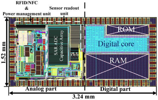
Figure 19.
Computer aided design (CAD) view of the complete layout of the SoC.

Table 5.
Design detail of the digital layout.
6. Functional Verification and Testing
The RFID/NFC communication and power management unit is realized as a stand-alone chip and is tested for full functionality. The power rectifier of the power supply and management unit has a measured power conversion efficiency of 45% (max) for a load of .The communication unit is designed in conformation to the ISO 15693/NFC 5 standard. The overall power consumption of the standalone chip is which is least in comparison to some other state-of-the-art ICs [30,31,32,76,77].
For the sensor readout unit, post layout mixed signal simulation is done to test the full functionalities.
To test the compatibility between the analog and the digital part, an FPGA (Field Programmable Gate Array) evaluation board is used which is marked as ’SIRIUS eval board’ in Figure 20. The evaluation board is further interfaced with the analog circuit interface board designed using discrete components. The analog circuit interface board consists of RFID/NFC communication unit, sensor interface unit and ADC. A post-layout simulation is carried out with the extracted netlist for the digital part after the final layout is accomplished. For the post-layout simulation, internal RAM and ROM and the external SPI flash device containing the application firmware is included to test the real-time functionalities. Table 6 gives an overview of the complete design of the SoC.

Figure 20.
Left hand side: RFID/NFC communication and sensor readout board is shown. Right hand side: The SIRIUS evaluation board together with the interface board.

Table 6.
SoC—Key design parameters.
To the best knowledge of the authors, an exactly similar SoC is unavailable for comparison which possesses all the features discussed in this paper. Table 7 presents a comparative view of the related works in this field. The work presented in [10] is an NFC enabled SoC which uses the communication protocol of ISO 15693 standard. The application area of the SoC is limited to glucose sensor measurement. A very similar application type SoC is discussed in [12] , but is incompatible with RFID/NFC communication protocol, besides it does not include an integrated microcontroller. Nevertheless, values presented by other works in the table are measured, while in this work only simulation values are presented.

Table 7.
Comparison with related works.
The particular advantage of the SoC is that it is programmable. The firmware can be customized; the PGA and the SAR ADC can be reconfigured based on the application specific requirement. The supply voltage is in the range of –. This makes it compatible with commercially available external devices like temperature or pressure sensors or external memory devices like Flash or FRAM. A JTAG (joint test action group) boundary scan is included, for on-chip debugging. The sensor readout part is only activated whenever it is required to make a measurement otherwise, it is kept isolated from the power supply, this reduces the static power consumption.
Next step is the comprehensive functional tests of the SoC after fabrication and the implementation of the proposed blood pressure monitoring implant. In this respect, the present research work includes a selection of the antenna design and the pressure sensor which is suitable to operate in the human body environment. The complete mechanical construction and biocompatible encapsulation of the implant are part of the future research.
7. Conclusions
A low power mixed-signal passive programmable SoC is presented in this paper. The design is implemented in a CMOS technology, on a die area of × —which includes the pads. The analog front-end consists of circuitries required for RFID/NFC communication and sensor readout. The digital part consists of a 32-bit RISC microcontroller along with other digital peripherals. The SoC has 16 KB of RAM and ROM as internal memory devices. It is a passive SoC which uses inductive coupling to power the entire sensor tags developed using the SoC. It uses a carrier frequency of 13.56 MHz in compliance with ISO 15693 or NFC5 standard. The complete integration of the microcontroller along with the analog part for communication and sensor readout is useful for small size, low cost, and low power sensor applications. The application area can be a temperature measurement for industrial applications or a bioimplant to measure blood pressure or ECG. The complete measurement of the chip after fabrication and realization of the proposed implant discussed in the paper is part of the future work.
Acknowledgments
The authors would like to thank Benjamin Dusch for his help in the layout and designing of the SoC. Authors will also like to thank MPC (Multi Project Chip) group for the funding of the chip fabrication.
Author Contributions
Mayukh Bhattacharyya is the main author and is responsible for writing the paper. Waldemar Gruenwald has provided valuable inputs for the design of the digital part and has also contributed substantially for writing the same. Dirk Jansen and Leonhard Reindl are responsible for providing valuable suggestions during the design phase and also while preparing the manuscript. Jasmin Aghassi-Hagmann is responsible with the proof read and formatting of the paper.
Conflicts of Interest
The authors declare no conflict of interest.
References
- Leon-Chaffee, E.; Light, R.U. A method for the remote control of electrical stimulation of the nervous system. Yale J. Biol. Med. 1949, 7, 83–128. [Google Scholar]
- Breakell, C.C.; Manc, L.D.S.; Parker, C.S.; Christopherson, F. Radio transmission of the human electroencephalogram and other electrophysiological data. Electroencephalogr. Clin. Nerophysiol. 1949, 1, 243–244. [Google Scholar]
- Farrar, J.T.; Zworykin, V.K. Pressure-Sensitive Telemetering Capsule for Study of Gastrointestinal Motility. Science 1957, 126, 975–976. [Google Scholar] [CrossRef] [PubMed]
- Cardullo, M.W. Transponder Apparatus and System. U.S. Patent 3,713,148 A, 23 January 1973. [Google Scholar]
- Landt, J. Shrouds of Time: The History of RFID; AIM: Pittsburgh, PA, USA, 2001; pp. 8–11. [Google Scholar]
- Wang, D.; Hu, J.; Tan, H.Z. A Highly Stable and Reliable 13.56-MHz RFID Tag IC for Contactless Payment. IEEE Trans. Ind. Electron. 2015, 62, 545–554. [Google Scholar] [CrossRef]
- Volk, T.; Gorbey, S.; Bhattacharyya, M.; Grünwald, W.; Lemmer, B.; Reindl, L.M.; Stieglitz, T.; Jansen, D. RFID Technology for Continuous Monitoring of Physiological Signals in Small Animals. IEEE Trans. Biomed. Circuits Syst. 2015, 62, 4365–4373. [Google Scholar] [CrossRef] [PubMed]
- Xiao, Z.; Tan, X.; Chen, X.; Chen, S.; Zhang, Z.; Zhang, H.; Wang, J.; Huang, Y.; Zhang, P.; Zheng, L.; et al. An Implantable RFID Sensor Tag toward Continuous Glucose Monitoring. IEEE Trans. Biomed. Circuits Syst. 2015, 19, 910–919. [Google Scholar] [CrossRef] [PubMed]
- 1974: DigitalWatch is First System-On-Chip Integrated Circuit. Available online: http://www.computerhistory.org/ (accessed on 03.11.2017).
- DeHennis, A.; Getzlaff, S.; Grice, D.; Mailand, M. An NFC-Enabled CMOS IC for a Wireless Fully Implantable Glucose Sensor. IEEE J. Biomed. Health Inform. 2016, 20, 18–28. [Google Scholar] [CrossRef] [PubMed]
- Cheong, J.H.; Yan Ng, S.S.; Liu, X.; Xue, R.-F.; Jen Lim, H.; Basappa Khannur, P.; Lim Chan, K.; Astuti Lee, A.; Kang, K.; Shiah Lim, L.; et al. An Inductively Powered Implantable Blood Flow Sensor Microsystem for Vascular Grafts. IEEE Trans. Biomed. Eng. 2012, 59, 2466–2475. [Google Scholar] [CrossRef] [PubMed]
- Huang, Y.J.; Tzeng, T.H.; Lin, T.W.; Huang, C.W.; Yen, P.W.; Kuo, P.H.; Lin, C.T.; Lu, S.S. A Self-Powered CMOS Reconfigurable Multi-Sensor SoC for Biomedical Applications. IEEE J. Solid-State Circuits 2014, 49, 851–866. [Google Scholar] [CrossRef]
- Zhang, Y.; Zhang, F.; Shakhsheer, Y.; Silver, J.D.; Klinefelter, A.; Nagaraju, M.; Boley, J.; Pandey, J.; Shrivastava, A.; Carlson, E.J.; et al. A Batteryless 19 μW MICS/ISM-Band Energy Harvesting Body Sensor Node SoC for ExG Applications. IEEE J. Solid-State Circuits 2013, 48, 199–213. [Google Scholar]
- Sharma, A.; Polley, A.; Lee, S.; Narayanan, S.; Li, W.; Sculley, T.; Ramaswamy, S. A Sub-60-μA Multimodal Smart Biosensing SoC with >80-dB SNR, 35-μA Photoplethysmography Signal Chain. IEEE J. Solid-State Circuits 2017, 52, 1021–1033. [Google Scholar] [CrossRef]
- Yip, M.; Jin, R.; Heidi Nakajima, H.; Stankovic, K.M.; Chandrakasan, A.P. A Fully-Implantable Cochlear Implant SoC With Piezoelectric Middle-Ear Sensor and Arbitrary Waveform Neural Stimulation. IEEE J. Solid-State Circuits 2015, 50, 214–229. [Google Scholar] [CrossRef] [PubMed]
- Khayatzadeh, M.; Zhang, X.; Tan, J.; Liew, W.-S.; Lian, Y. A 0.7-V 17.4-μW 3-Lead Wireless ECG SoC. IEEE Trans. Biomed. Circuits Syst. 2013, 7, 583–592. [Google Scholar] [CrossRef] [PubMed]
- Bhattacharyya, M.; Grünwald, W.; Dusch, B.; Aghassi-Hagmann, J.; Jansen, D.; Reindl, L. A RFID/NFC based Programmable SoC for biomedical applications. In Proceedings of the International SoC Design Conference (ISOCC), Jeju, Korea, 3–6 November 2014; pp. 80–81. [Google Scholar]
- Bhattacharyya, M.; Dusch, B.; Jansen, D.; Mackensen, E. Design and Verification of a Mixed-Signal SoC for Biomedical Applications; Hochschule Ulm: Ulm, Germany, 2015; pp. 43–48. ISSN 1868-9221. [Google Scholar]
- Nehler, M.R.; Duval, S.; Diao, L.; Annex, B.H.; Hiatt, W.R.; Rogers, K.; Zakharyan, A.; Hirsch, A.T. Epidemiology of peripheral arterial disease and critical limb ischemia in an insured national population. J. Vasc. Surg. 2014, 60, 686–695. [Google Scholar] [CrossRef] [PubMed]
- Anderson, J.L.; Halperin, J.L.; Albert, N.M.; Bozkurt, B.; Brindis, R.G.; Curtis, L.H.; DeMets, D.; Guyton, R.A.; Hochman, J.S.; Kovacs, R.J.; et al. Management of Patients With Peripheral Artery Disease. J. Am. Coll. Cardiol. 2013, 127, 1425–1443. [Google Scholar]
- Fowkes, F.-G.R.; Rudan, D.; Rudan, I.; Aboyans, V.; Denenberg, J.O.; McDermott, M.M.; Norman, P.E.; Sampson, U.K.A.; Williams, L.J.; Mensah, G.A.; et al. Comparison of global estimates of prevalence and risk factors for peripheral artery disease in 2000 and 2010: A systematic review and analysis. Lancet 2013, 382, 1329–1338. [Google Scholar] [CrossRef]
- Federal Communications Commission. FCC Body Tissue Dielectric Parameters; Federal Communications Commission: Washington, DC, USA, 2017.
- Alioto, M. Ultra-Low Power VLSI Circuit Design Demystified and Explained: A Tutorial. IEEE Trans. Circuits Syst. I Regul. Pap. 2012, 59, 3–29. [Google Scholar] [CrossRef]
- Sarpeshkar, R. Universal Principles for Ultra Low Power and Energy Efficient Design. IEEE Trans. Circuits Syst. II 2012, 59, 193–198. [Google Scholar] [CrossRef]
- Tajalli, A.; Leblebici, Y. Design Trade-offs in Ultra-Low-Power Digital Nanoscale CMOS. IEEE Trans. Circuits Syst. I Regul. Pap. 2011, 58, 2189–2200. [Google Scholar] [CrossRef]
- Lundager, K.; Zeinali, B.; Tohidi, M.; Madsen, J.K.; Moradi, F. Low Power Design for FutureWearable and Implantable Devices. J. Low Power Electron. Appl. 2016, 6, 20. [Google Scholar] [CrossRef]
- Comer, D.J.; Comer, D.T. Using the Weak Inversion Region to Optimize Input Stage Design of CMOS Op Amps. IEEE Trans. Circuits Syst. II 2004, 51, 8–14. [Google Scholar] [CrossRef]
- Rabaey, J. Low Power Design Essentials; Springer: Berlin, Germany, 2009. [Google Scholar]
- Lotze, N.; Manoli, Y. Ultra-Sub-Threshold Operation of Always-On Digital Circuits for IoT Applications by Use of Schmitt Trigger Gates. IEEE Trans. Circuits Syst. I Regul. Pap. 2017, 64, 2920–2933. [Google Scholar] [CrossRef]
- Lu, C.; Li, J.-A.; Lin, T.H. A 13.56-MHz passive (NFC) tag IC in 0.18-μm CMOS process for biomedical applications. In Proceedings of the International Symposium on VLSI Design, Automation and Test (VLSI-DAT), Hsinchu, Taiwan, 25–27 April 2016; pp. 1–4. [Google Scholar]
- Lee, J.W.; Vo, D.; Hong, S.H.; Huynh, Q.H. A fully integrated high security NFC target IC using 0.18 μm CMOS process. In Proceedings of the ESSCIRC (ESSCIRC), Helsinki, Finland, 12–16 September 2011; pp. 551–554. [Google Scholar]
- Lee, J.W.; Vo, D.H.T.; Huynh, Q.H.; Hong, S.H. A Fully Integrated HF-Band Passive RFID Tag IC Using 0.18 μm CMOS Technology for Low-Cost Security Applications. IEEE Trans. Ind. Electron. 2011, 58, 2531–2540. [Google Scholar]
- Dongsheng, L.; Huan, L.; Xuecheng, Z.; Liang, G.; Ke, Y.; Zilong, L. A High Sensitivity Analog Front-end Circuit for Semi-Passive HF RFID Tag Applied to Implantable Devices. IEEE Trans. Circuits Syst. I Regul. Pap. 2015, 62, 1991–2002. [Google Scholar] [CrossRef]
- Haddad, P.A.; Gosset, G.; Raskin, J.P.; Flandre, D. Automated Design of a 13.56 MHz 19 μW Passive Rectifier with 72% Efficiency Under 10 μA load. IEEE J. Solid-State Circuits 2016, 51, 1290–1301. [Google Scholar] [CrossRef]
- Li, X.; Tsui, C.-Y.; Ki, W.-H. A 13.56 MHz Wireless Power Transfer System With Reconfigurable Resonant Regulating Rectifier and Wireless Power Control for Implantable Medical Devices. IEEE J. Solid-State Circuits 2015, 50, 978–989. [Google Scholar] [CrossRef]
- Hashemi, S.; Sawan, M.; Savaria, Y. A High-Efficiency Low-Voltage CMOS Rectifier for Harvesting Energy in Implantable Devices. IEEE Trans. Biomed. Circuits Syst. 2012, 6, 326–335. [Google Scholar] [CrossRef] [PubMed]
- Duan, Q.; Roh, J. A 1.2-V 4.2-ppm/°C High-Order Curvature-Compensated CMOS Bandgap Reference. IEEE Trans. Circuits Syst. I Regul. Pap. 2015, 62, 662–670. [Google Scholar] [CrossRef]
- Abbasi, M.U.; Raikos, G.; Saraswat, R.; Rodriguez-Villegas, E. A high PSRR, ultra-low power 1.2 V curvature corrected Bandgap Reference for Wearable EEG application. In Proceedings of the IEEE 13th International New Circuits and Systems Conference (NEWCAS), Grenoble, France, 7–10 June 2015; pp. 1–4. [Google Scholar]
- Ma, B.; Yu, F. A Novel 1.2-V 4.5-ppm/°C Curvature-Compensated CMOS Bandgap Reference. IEEE Trans. Circuits Syst. I Regul. Pap. 2014, 61, 1026–1035. [Google Scholar] [CrossRef]
- Tsividis, Y.P. Accurate analysis of temperature effects in IC/-VBE characteristics with application to bandgap reference sources. IEEE J. Solid-State Circuits 1980, 15, 1076–1084. [Google Scholar] [CrossRef]
- Widlar, R.J. New developments in IC voltage regulators. IEEE J. Solid-State Circuits 1971, 6, 2–7. [Google Scholar] [CrossRef]
- Wang, B.; Law, M.K.; Bermak, A.; Luong, H.C. A Passive RFID Tag Embedded Temperature Sensor With Improved Process Spreads Immunity for a 30 °C to 60 °C Sensing Range. IEEE Trans. Circuits Syst. I Regul. Pap. 2014, 61, 337–346. [Google Scholar] [CrossRef]
- Maity, A.; Patra, A. A Single-Stage Low-Dropout Regulator With a Wide Dynamic Range for Generic Applications. IEEE Trans. Very Large Scale Integr. (VLSI) Syst. 2016, 24, 2117–2127. [Google Scholar] [CrossRef]
- Huang, C.H.; Ma, Y.T.; Liao, W.C. Design of a Low-Voltage Low-Dropout Regulator. IEEE Trans. Very Large Scale Integr. (VLSI) Syst 2014, 22, 1308–1313. [Google Scholar] [CrossRef]
- Heng, S.; Pham, C.K. A Low-Power High-PSRR Low-Dropout Regulator With Bulk-Gate Controlled Circuit. IEEE Trans. Circuits Syst. II 2010, 57, 245–249. [Google Scholar] [CrossRef]
- Lau, S.K.; Mok, P.K.T.; Leung, K.N. A Low-Dropout Regulator for SoC With Q-Reduction. IEEE J. Solid-State Circuits 2007, 42, 658–664. [Google Scholar] [CrossRef]
- Dusch, B. Entwicklung und Layout Eines Analog-Digital-Wandlers mit 12 Bit Auflösung in Einer 180 nm-CMOS-Zieltechnologie. Master’s Thesis, University of Applied Sciences, Offenburg, Germany, 2014. [Google Scholar]
- Melek, L.A.P.; da Silva, A.L.; Schneider, M.C.; Galup-Montoro, C. Analysis and Design of the Classical CMOS Schmitt Trigger in Subthreshold Operation. IEEE Trans. Circuits Syst. I Regul. Pap. 2017, 64, 869–878. [Google Scholar] [CrossRef]
- Dusch, B.; Bhattacharyya, M.; Jansen, D. Entwicklung und Layoutentwurf Eines Analog-Digital-Wandlers mit 12 Bit Auflösung in Einer 180 nm-CMOS-Technologie; Hochschule Ulm: Ulm, Germany, February 2015; pp. 13–21. ISSN 1868-9221. [Google Scholar]
- Butti, F.; Piotto, M.; Bruschi, P. A Chopper Instrumentation Amplifier With Input Resistance Boosting by Means of Synchronous Dynamic Element Matching. IEEE Trans. Circuits Syst. I Regul. Pap. 2017, 64, 753–764. [Google Scholar] [CrossRef]
- Worapishet, A.; Demosthenous, A.; Liu, X. A CMOS Instrumentation Amplifier with 90-dB CMRR at 2-MHz Using Capacitive Neutralization: Analysis, Design Considerations, and Implementation. IEEE Trans. Circuits Syst. I Regul. Pap. 2011, 58, 699–710. [Google Scholar] [CrossRef]
- Wu, R.; Makinwa, K.A.A.; Huijsing, J.H. A Chopper Current-Feedback Instrumentation Amplifier With a 1 MHz 1/f Noise Corner and an AC-Coupled Ripple Reduction Loop. IEEE J. Solid-State Circuits 2009, 44, 3232–3243. [Google Scholar] [CrossRef]
- Saberi, M.; Lotfi, R.; Mafinezhad, K.; Serdijn, W.A. Analysis of Power Consumption and Linearity in Capacitive Digital-to-Analog Converters Used in Successive Approximation ADCs. IEEE Trans. Circuits Syst. I Regul Pap. 2011, 58, 1736–1748. [Google Scholar] [CrossRef]
- Zhu, Z.; Liang, Y. A 0.6-V 38-nW 9.4-ENOB 20-kS/s SAR ADC in 0.18-μm CMOS for Medical Implant Devices. IEEE Trans. Circuits Syst. I Regul. Pap. 2015, 62, 2167–2176. [Google Scholar] [CrossRef]
- Nandi, P.; Talukdar, H.; Kumar, D.; Kumar, A.; Katakwar, G. A Novel Approach to Design SAR-ADC: Design Partitioning Method. IEEE Tran. Comput.-Aided Des. Integr. Circuits Syst. 2016, 35, 1277–1287. [Google Scholar] [CrossRef]
- Rahiminejad, E.; Saberi, M.; Lotfi, R. A Power-Efficient Signal-Specific ADC for Sensor-Interface Applications. IEEE Trans. Circuits Syst. II 2017, 64, 1032–1036. [Google Scholar] [CrossRef]
- Venuto, D.E.; Castro, D. Ultra low-power 12 bit SAR ADC for RFID Aapplications. In Proceedings of the Design, Automation and Test in Europe Conference and Exhibition, Dresden, Germany, 8–12 March 2010; pp. 1071–1075. [Google Scholar]
- Van Elzakker, M.; van Tuijl, E.; Geraedts, P.; Schinkel, D.; Klumperink1, E.; Nauta1, B. A 1.9 μW 4.4fJ/Conversion-step 10b 1MS/s Charge-Redistribution ADC. In Proceedings of the IEEE International Solid-State Circuits Conference Digest of Technical Papers (ISSCC), San Francisco, CA, USA, 3–7 February 2008; pp. 244–245. [Google Scholar]
- Lin, K.T.; Cheng, Y.W.; Tang, K.T. A 0.5 V 1.28-MS/s 4.68-fJ/Conversion-Step SAR ADC with Energy-Efficient DAC and Trilevel Switching Scheme. IEEE Trans. Very Large Scale Integr. (VLSI) Syst. 2016, 24, 1441–1449. [Google Scholar] [CrossRef]
- Huang, G.Y.; Chang, S.J.; Liu, C.-C.; Lin, Y.Z. 10-bit 30-MS/s SAR ADC Using a Switchback Switching Method. IEEE Trans. Very Large Scale Integr. (VLSI) Syst. 2013, 21, 584–588. [Google Scholar] [CrossRef]
- Zhang, D.; Bhide, A.; Alvandpour, A. A 53-nW 9.1-ENOB 1-kS/s SAR ADC in 0.13-μm CMOS for Medical Implant Devices. IEEE J. Solid-State Circuits 2012, 47, 1585–1595. [Google Scholar] [CrossRef]
- Cho, S.H.; Lee, C.K.; Lee, S.G.; Ryu, S.T. A Two-Channel Asynchronous SAR ADC With Metastable-Then-Set Algorithm. IEEE Trans. Very Large Scale Integr. (VLSI) Syst. 2012, 20, 765–769. [Google Scholar] [CrossRef]
- Harpe, P.J.A.; Zhou, C.; Bi, Y.; van der Meijs, N.P.; Wang, X.; Philips, K.; Dolmans, G.; de Groot, H. A 26 μW 8 bit 10 MS/s Asynchronous SAR ADC for Low Energy Radios. IEEE J. Solid-State Circuits 2011, 46, 1585–1595. [Google Scholar]
- Lee, S.K.; Park, S.J.; Park, H.J.; Sim, J.Y. A 21 fJ/Conversion-Step 100 kS/s 10-bit ADC With a Low-Noise Time-Domain Comparator for Low-Power Sensor Interface. IEEE J. Solid-State Circuits 2011, 46, 651–659. [Google Scholar] [CrossRef]
- Zhu, Y.; Chan, C.-H.; Chio, U.-F.; Sin, S.-W.; Seng-Pan, U.; Martins, R.P.; Maloberti, F. A 10-bit 100-MS/s Reference-Free SAR ADC in 90 nm CMOS. IEEE J. Solid-State Circuits 2010, 45, 1111–1121. [Google Scholar] [CrossRef]
- Ahmadi, M.; Namgoong, W. Comparator Power Minimization Analysis for SAR ADC Using Multiple Comparators. IEEE Trans. Circuits Syst. I Regul. Pap. 2015, 62, 2369–2379. [Google Scholar] [CrossRef]
- Verma, N.; Chandrakasan, A.P. An Ultra Low Energy 12-bit Rate-Resolution Scalable SAR ADC for Wireless Sensor Nodes. IEEE J. Solid-State Circuits 2007, 42, 1196–1205. [Google Scholar] [CrossRef]
- Fredenburg, J.A.; Flynn, M.P. Statistical Analysis of ENOB and Yield in Binary Weighted ADCs and DACS With Random Element Mismatch. IEEE Trans. Circuits Syst. I Regul. Pap. 2012, 59, 1396–1408. [Google Scholar] [CrossRef]
- Lee, Y.; Song, J.; Park, I.C. Statistical modeling of capacitor mismatch effects for successive approximation register ADCs. In Proceedings of the International SoC Design Conference (ISOCC), Jeju, Korea, 17–18 November 2011; pp. 302–305. [Google Scholar]
- Haenzsch, S.; Henker, S.; Schüffny, R. Modelling of Capacitor Mismatch and Non-Linearity Effects in Charge Redistribution SAR ADCs. In Proceedings of the 17th International Conference Mixed Design of Integrated Circuits and Systems (MIXDES), Wroclaw, Poland, 24–26 June 2010; pp. 300–305. [Google Scholar]
- Tripathi, V.; Murmann, B. Mismatch Characterization of Small Metal Fringe Capacitors. IEEE Trans. Circuits Syst. I Regul. Pap. 2014, 61, 2236–2242. [Google Scholar] [CrossRef]
- Li, Y.; Zhang, Z.; Chua, D.; Lian, Y. Placement for Binary-Weighted Capacitive Array in SAR ADC Using Multiple Weighting Methods. IEEE Tran. Comput.-Aided Des. Integr. Circuits Syst. 2014, 33, 1277–1287. [Google Scholar]
- Jansen, D.; Fawaz, N.; Bau, D.; Durrenberger, M. A small high performance microprocessor core SIRIUS for embedded low power designs, demonstrated in a medical mass application of an electronic pill (EPILLE). In Proceedings of the International Federation for Information Processing (IFIP), Portland, OR, USA, 29–31 July 2007; pp. 363–372, ISBN 978-0-387-72257-3. [Google Scholar]
- Fawaz, N.; Jansen, D. A SoC Electronic Pill (ePille®) with 32bit SIRIUS Processor and Bidirectional Communication System used for Biomedical Telemetry Applications. In Proceedings of the Information and Communication technologies (ICTTA), Damascus, Syria, 7–11 April 2008; pp. 1–3, ISBN 978-1-4244-1751-3. [Google Scholar]
- Roth, M. Redesign und Optimierung Eines 16/32-Bit Mikroprozessorkerns “SIRIUS Janua 2.0” in Formal Abstraker Codierung Sowie Verifikation in Einem Altera Cyclone FPGA. Master’s Thesis, University of Applied Sciences, Offenburg, Germany, 2012. [Google Scholar]
- Hwang, Y.S.; Lin, H.C. A New CMOS Analog Front End for RFID Tags. IEEE Trans. Ind. Electron. 2009, 56, 2299–2307. [Google Scholar] [CrossRef]
- Cho, J.H.; Kim, J.; Kim, J.W.; Lee, K.; Ahn, K.D.; Kim, S. An NFC transceiver with RF-powered RFID transponder mode. In Proceedings of the IEEE Asian Solid-State Circuits Conference, Jeju City, Korea, 12–14 November 2007; pp. 172–175. [Google Scholar]
© 2018 by the authors. Licensee MDPI, Basel, Switzerland. This article is an open access article distributed under the terms and conditions of the Creative Commons Attribution (CC BY) license (http://creativecommons.org/licenses/by/4.0/).

