Abstract
This paper deals with the modeling of bond graph buck converter systems. The bond graph formalism, which represents a heterogeneous formalism for physical modeling, is used to design a sub-model of a power MOSFET and PiN diode switchers. These bond graph models are based on the device’s electrical elements. The application of these models to a bond graph buck converter permit us to obtain an invariant causal structure when the switch devices change state. This paper shows the usefulness of the bond graph device’s modeling to simulate an implicit bond graph buck converter.
1. Introduction
A bond graph is a physics-based modeling tool that provides an energy-based topological framework for the modeling of physical systems [1]. It enhances the visual understanding of these systems through the visual indication of the cause and effect relationships of the energy transfer between the subsystem variables. A bond graph, as a powerful modeling tool, has known great development and enjoyed a well-deserved popularity in many engineering disciplines.
Regarding the power converter modeling discipline, recent research has begun to overcome the problem of switching and state discontinuities. In [2], a new bond graph element to represent an ideal switch was proposed. In this method, the switching operation is handled by sending, on a junction, zero flow when the switch is ON and zero effort when the switch is OFF. This method needs a reconfiguration of the causality whenever the position of the switchers changes. An extension of this method is the causality resistor technique [3] that suggests the addition of a resistor to the switch port. The adaptation of the causality of this resistor according to the ideal switch state leads to unchanged causality for the rest of the bond graph diagram. Other models use the modulated transformer (MTF) [4,5], where a modulation parameter m is set to 1 for the closed switch state and to 0 for the open switch state, but the causality must be reassigned. An extension of this technique [3], taking account of the resistance of the switcher during the ON mode, consists in combining a Ron resistor to the MTF to represent the non-linear characteristics of the switcher. This method allows for the definition of a single bond graph model that holds for all switch positions. Another method that implies invariant causalities during the different switch modes is the switched power junction [5]. Here, more than one bond can decide the effort at a 0-junction and the flow at a 1-junction at mutual time instants. These techniques, however, do not show the dynamic internal comportment of the switch devices during their switching mode. In this respect, there are some works [6,7,8] where the authors developed new switcher component models based on the bond graph formalism for a better modeling of the internal physical behavior of these devices. In this paper, we present the dynamic models, by a bond graph formalism, of the power MOSFET transistor and the PiN diode and their application in a buck converter circuit. The use of these switcher models leads to unchanged causality during the different transition states, and to a better simulation of the dynamic comportment of the buck converter and the switcher devices.
To analyze the transfer of energy and the performance in a converter system against input or load changes, a PWM regulator block is always used. Therefore, the bond graph package was developed in the VHDL-AMS language. This is to design bond graph schema mixed with digital control blocks. This package was integrated into the graphical modeling tool SystemVision in order to explore rapid prototyping and the visual design facilities.
VHDL-AMS is a new mixed-signal modelling language based on the VHDL language. It is designed to support mixed-signal systems that contain digital elements and analog elements and to allow the interaction between them. It allows for hierarchy description and the simulation of continuous and discrete events [9,10].
This article is organized as follows. Section 2 introduces the bond graph theory. Section 3 describes the buck bond graph design methodology using a power MOSFET and a PiN diode bond graph sub-model. Section 4 presents the simulation results. Finally, the last section provides some conclusions and suggestions for future work.
2. The Bond Graph Theory
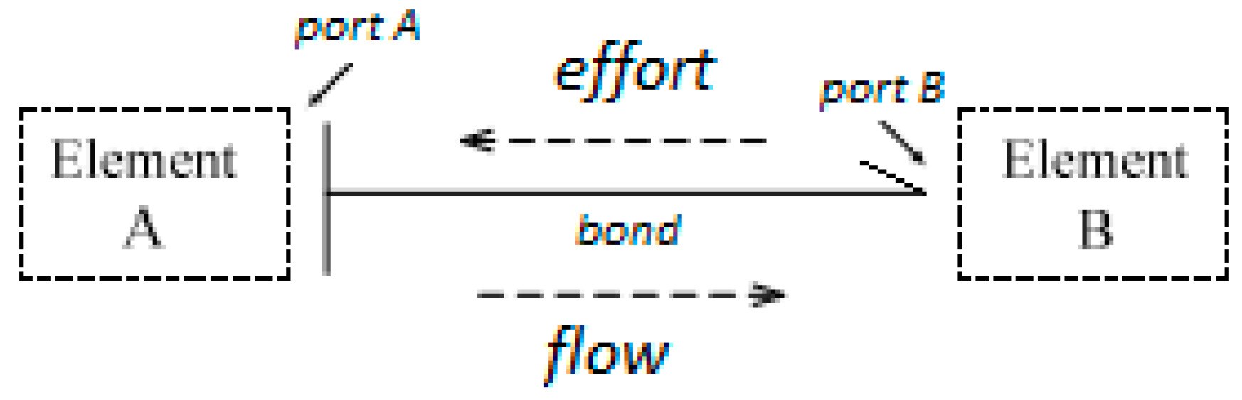
A bond graph is an engineering tool based on the description of physical systems by analyzing the exchange of energy within [1]. This exchange determines the dynamic behavior of the systems. Bond graph modeling involves devices, their connections, directed power transfers, and causality strokes. The power or the energy flow is represented by a half arrow called a power bond. Each bond is associated with two variables: effort and flow. The direction of the flow variable is given by the causality information. Graphically, the causality is indicated by putting a stroke near the element which controls the flow as shown in Figure 1.
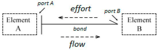
Figure 1.
The general conventions of bond causality.
The energy flow in a system is described at any time by the value of the power, which is the product of the effort variable by the flow variable. Therefore, a bond graph can represent systems from different domains in a unified way. Table 1 shows the effort and the flow variables of the main physical domains.

Table 1.
Effort and flow variables of the main physical domains.
3. The Buck Bond Graph Model
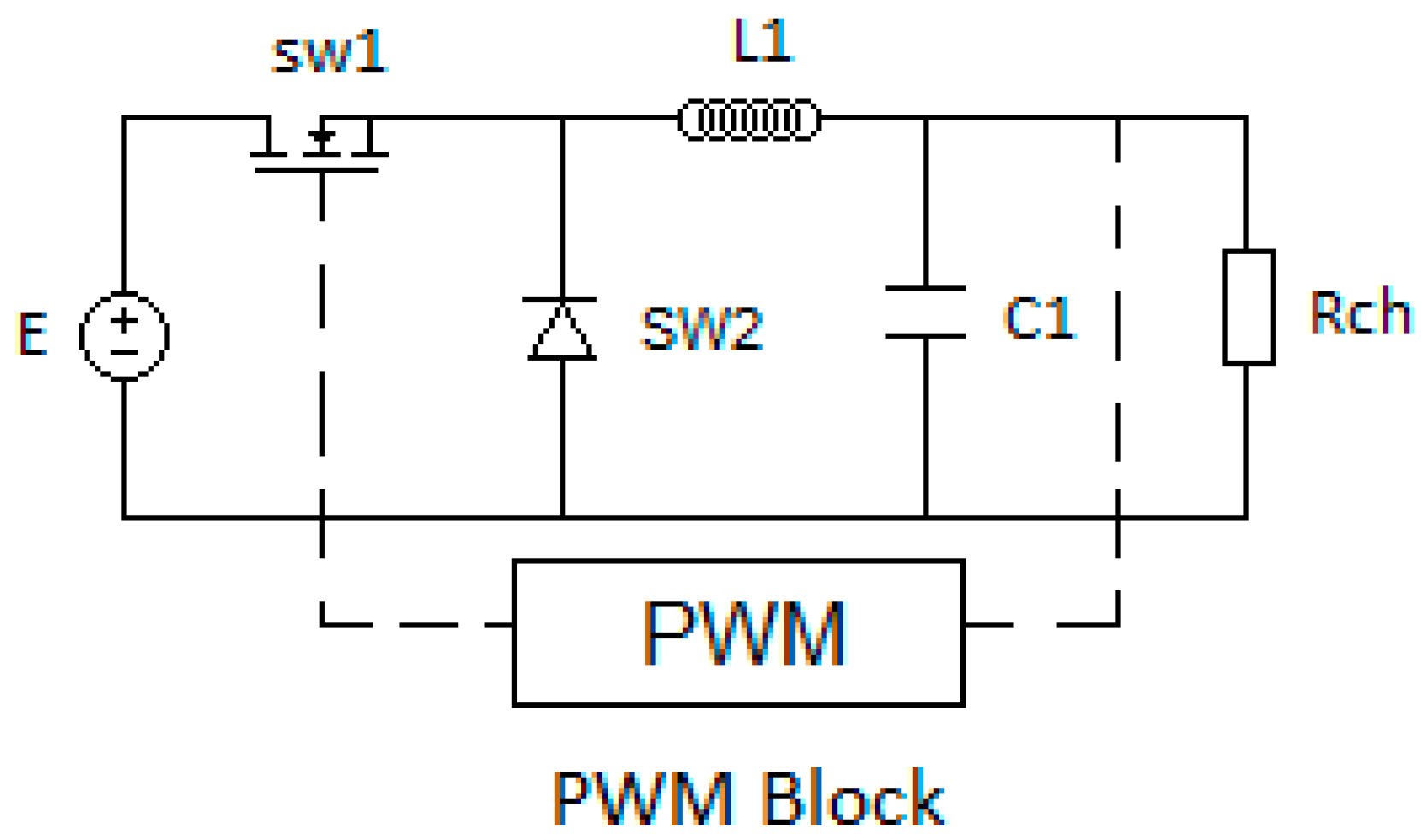
The buck converter to simulate is pictured in Figure 2. It consists of a switch-regulated buck converter, where the values of its components have been chosen as: voltage E = 9 Volts, L = 50 µH, C = 50 µF, and R = 4 Ohms. The switcher Sw1 represents the power MOSFET IRF740 and Sw2 represents the PiN diode STTA81200. In this example, the buck converter is chosen to operate in continuous conduction mode.
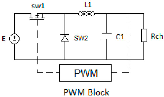
Figure 2.
Circuit diagram of the regulated buck converter.
To derive the buck bond graph schema, we designed the switchers’ bond graph sub-model and added them to the buck bond graph model with respect to the sequential causality assignment procedure.
3.1. Power MOSFET Bond Graph Sub-Model Description
Figure 3 shows the cross-section of the power MOSFET (VDMOS). The basic electrical components to satisfy its dynamic behavior are [11]:
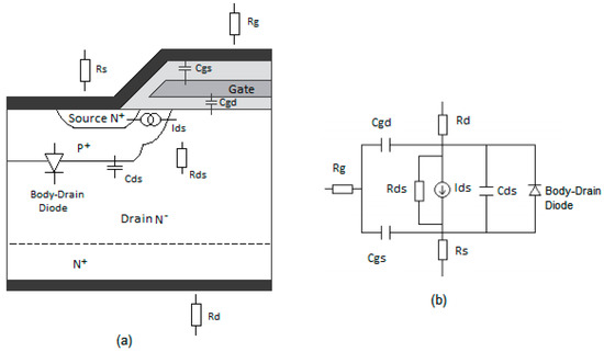
Figure 3.
(a) Cross-Section of Power MOSFET showing the principal electrical elements; (b) equivalent electrical schema of the Power MOSFET.
- The capacitances Cds, Cgd and Cgs that simulate the drain-source, gate-source, and gate-drain capacitances, respectively;
- The resistances Rd, Rg and Rs that represent the equivalent resistance of the drain, gate, and source, respectively;
- The resistance Rds that represents the total resistance between the drain and the source (the body-drain diode); and
- The controlled current source Ids, whose associated equations are:
Therefore, an equivalent bond graph model for the power MOSFET can be derived from these basic components.
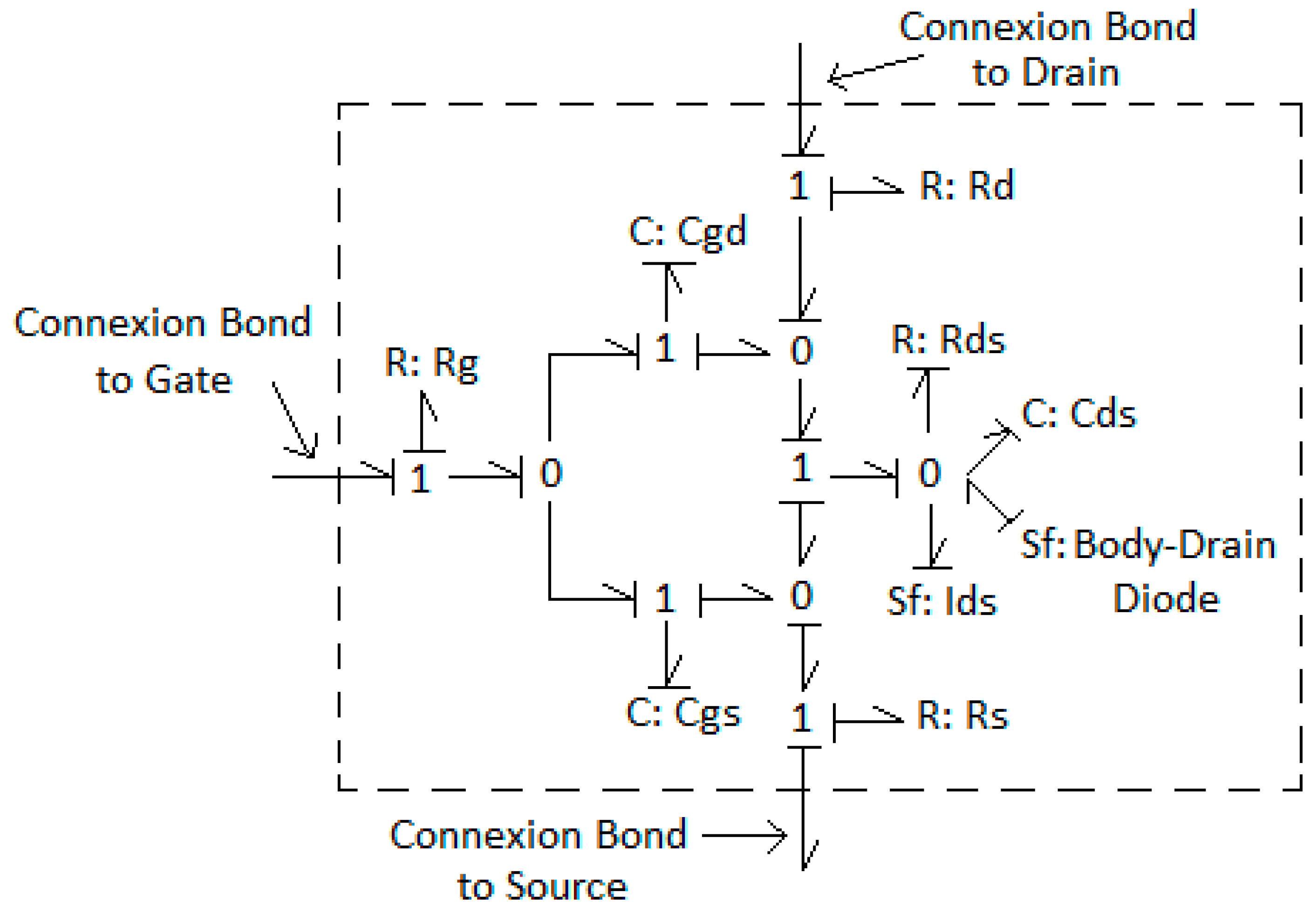
To derive the bond graph model of the power MOSFET, we used the 0-junction to represent the Kirchoff’s current law (the 0-junction is inserted at each node and between elements that have the same potential) and the 1-junction to represent Kirchoff’s voltage law (the 1-junction is inserted between the 0-junctions). For the assignment of the causality (Figure 4), we applied the sequential causality assignment procedure [1] in order to transfer the effort value (that is the voltage) from the drain and the source to the flow source element Ids. The value of the effort Vgs used on the flow source Ids is obtained from a voltage-to-quantity converter, placed at the gate bond, via an information link. Table 2 shows the values of the Power MOSFET IRF740 parameters.
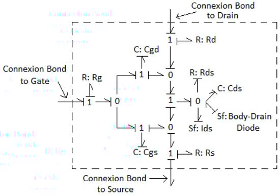
Figure 4.
Bond graph sub-model of the power MOSFET.
Table 2.
The Power MOSFET IRF740 Parameters.
3.2. PiN Diode Bond Graph Model Description
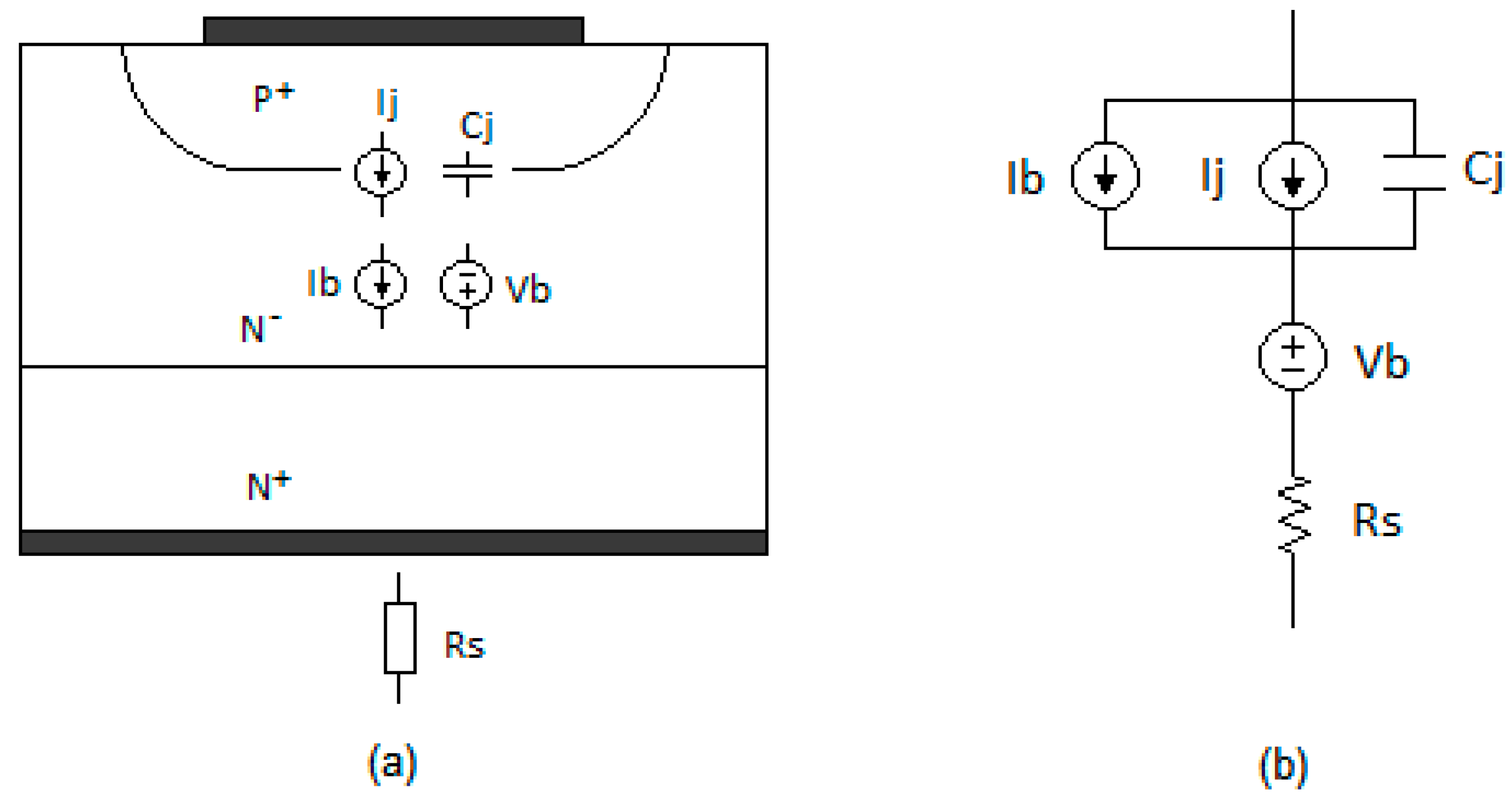
The Pin diode consists of a wide and lightly doped central region delimited by two generally much thinner and more highly doped lateral regions and (Figure 5). To model the dynamic comportment of the PiN diode, we use the following electrical components [12]:
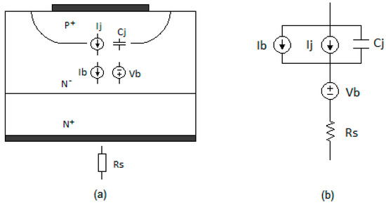
Figure 5.
(a) Cross-Section of PiN diode showing the principal electrical elements; (b) equivalent electrical schema of the PiN diode.
- The current junction source Ij defined by the following equation:where is the junction voltage and is the thermal voltage.
- The current base source Ib, whose relations are as follows:where is the injected charge level at the junction and is the total charge in the central region, where:and
- The voltage base source Vb, equal to:
- The junction capacitance Cj
- The equivalent resistance Rs
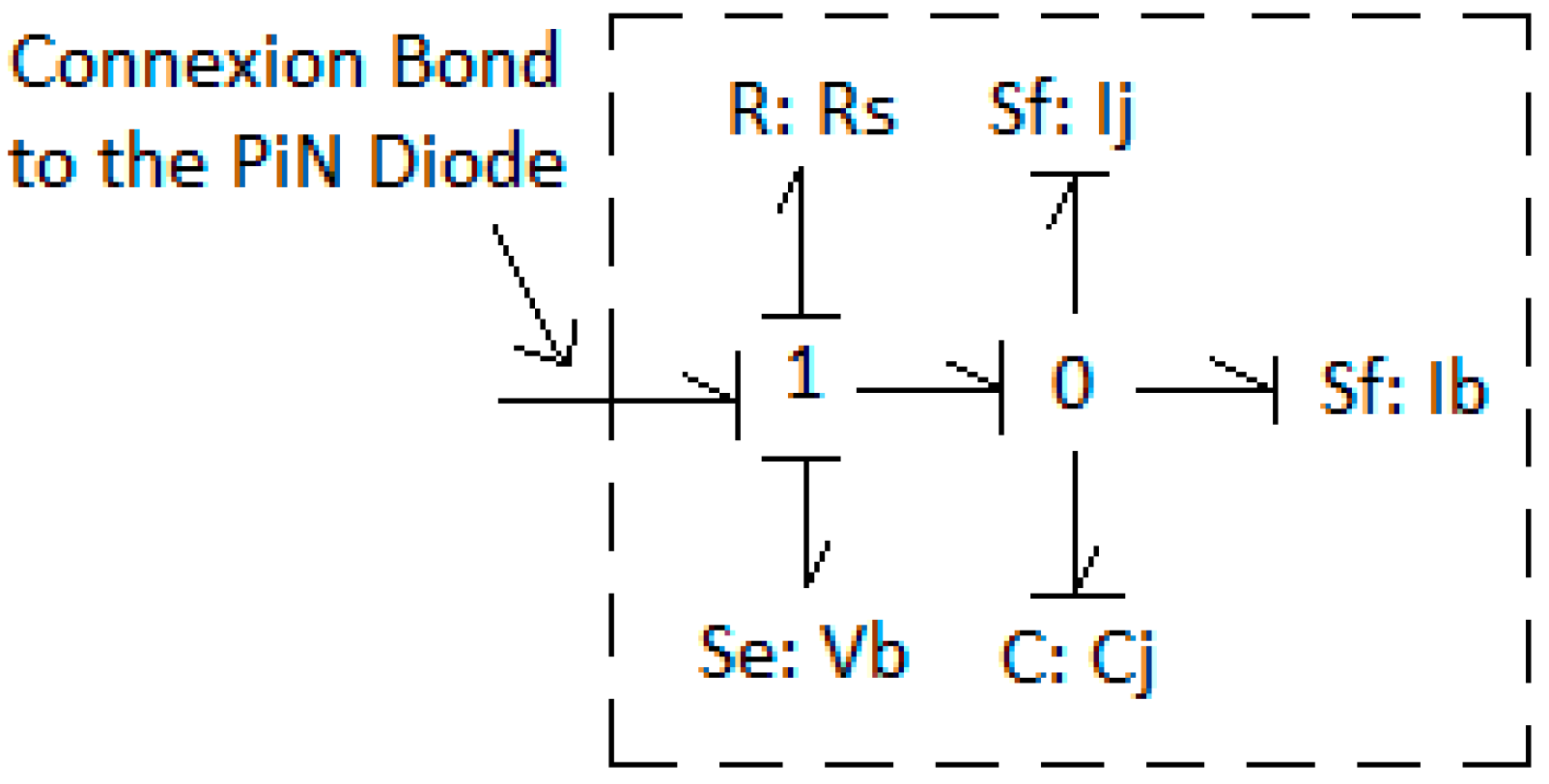
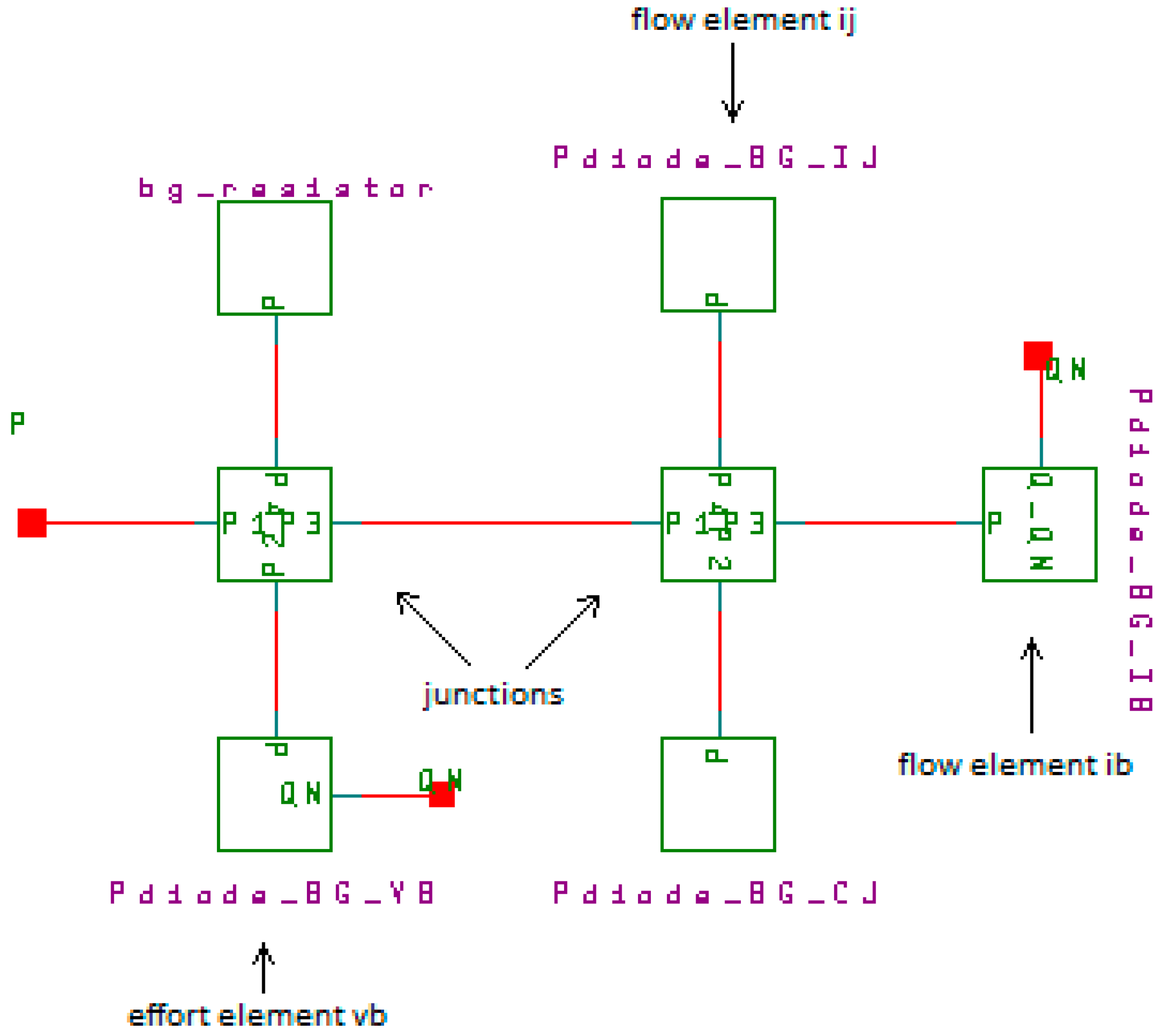
Based on the same procedure used in the case of the power MOSFET, we can derive the bond graph PiN diode sub-model as represented below in Figure 6. The parameters of the PiN diode STTA81200 are reported in Table 3.
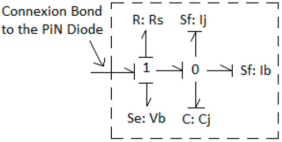
Figure 6.
Bond graph sub-model of the PiN diode.
Table 3.
The PiN diode STTA81200 Parameters.
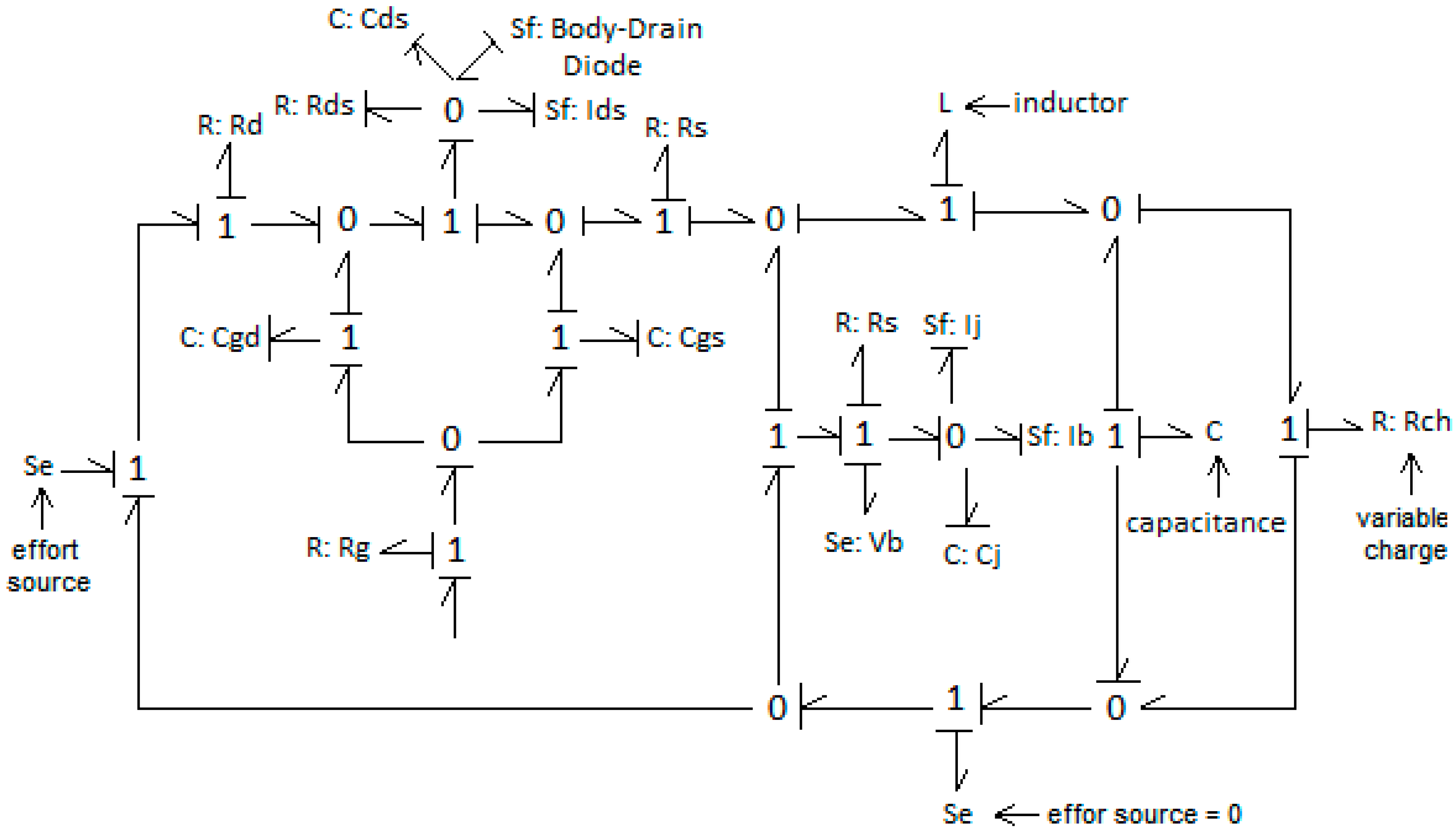
3.3. Derivation of the Buck Bond Graph Model
By applying the bond graph sub-model of the power MOSFET transistor and the PiN diode, and with respect to the sequential causality assignment procedure, the resulting buck bond graph model is as shown in Figure 7.
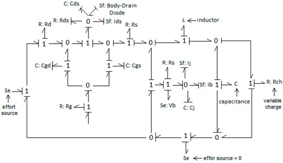
Figure 7.
Bond graph buck converter schema.
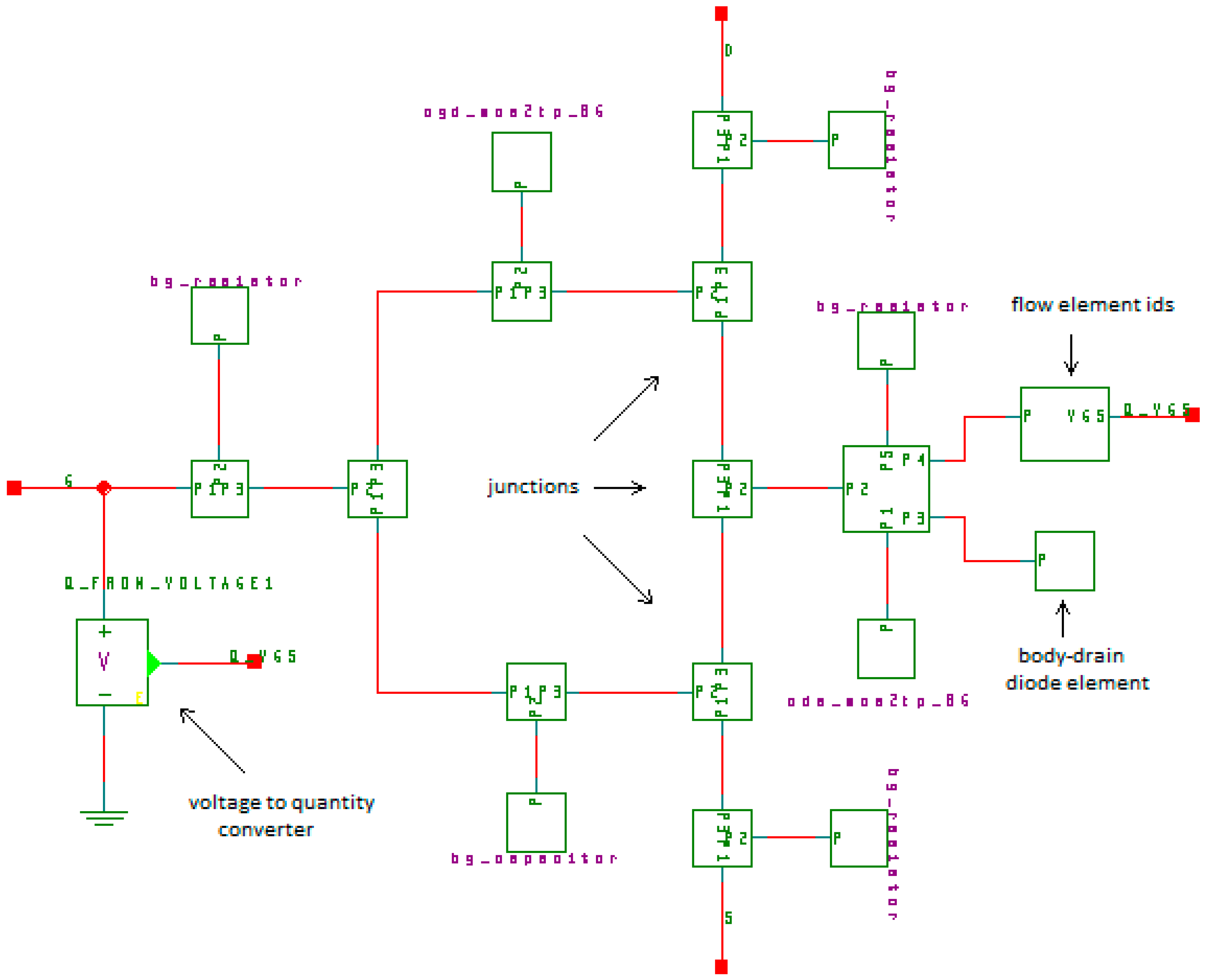
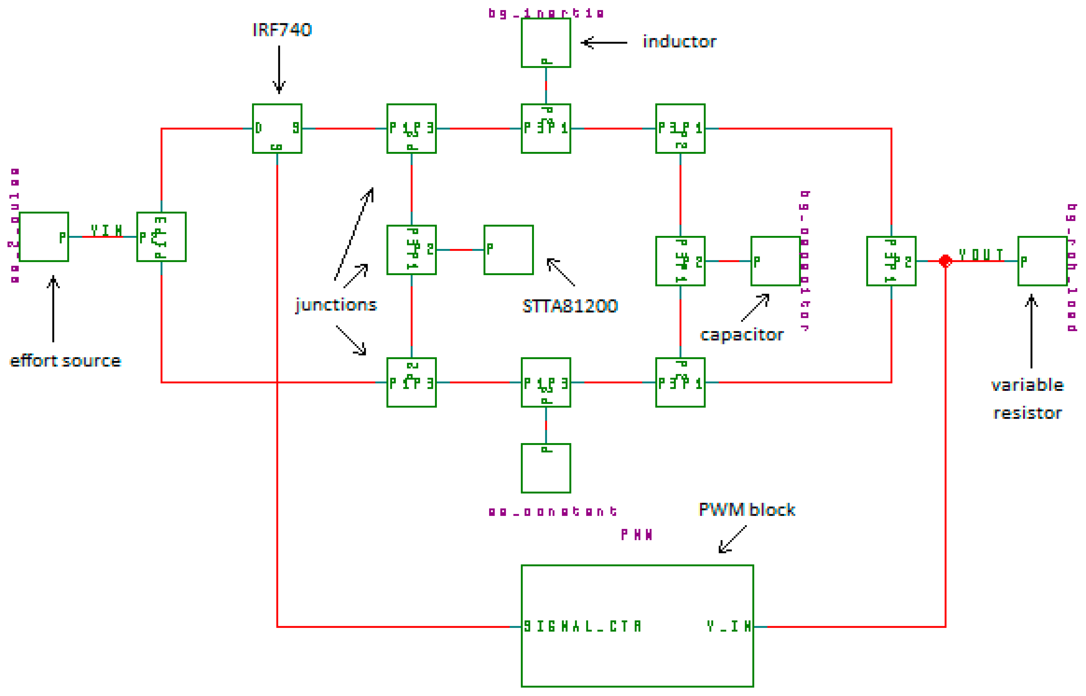
The implementation of the power-MOSFET, PiN diode, and the buck bond-graph model in SystemVision is achieved via the graphical and user-friendly interface (Figure 8, Figure 9 and Figure 10). In SystemVision, the designer can draw the bond graph model on the screen by using the basic bond graph library written in the VHDL-AMS language. For more information about the combination of bond graph theory and mixed language programming, the reader can refer to [13,14,15], and [15,16,17] for more detail about the implementation of the basic bond graph elements in VHDL-AMS.
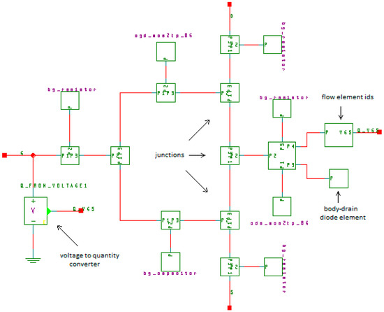
Figure 8.
Implementation of the power MOSFET bond graph sub-model in SystemVision.
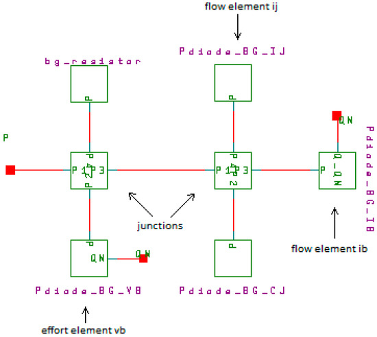
Figure 9.
Implementation of the PiN diode bond graph sub-model in SystemVision.
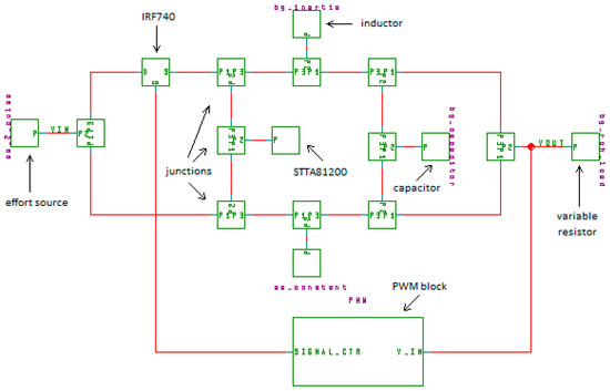
Figure 10.
Screen of SystemVision showing the buck bond graph model.
4. Simulation Results
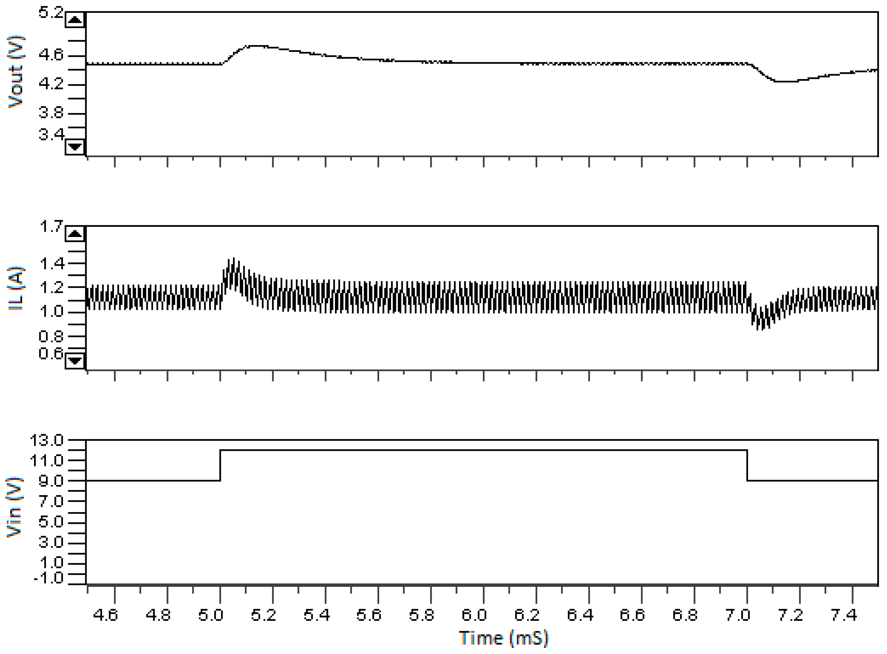
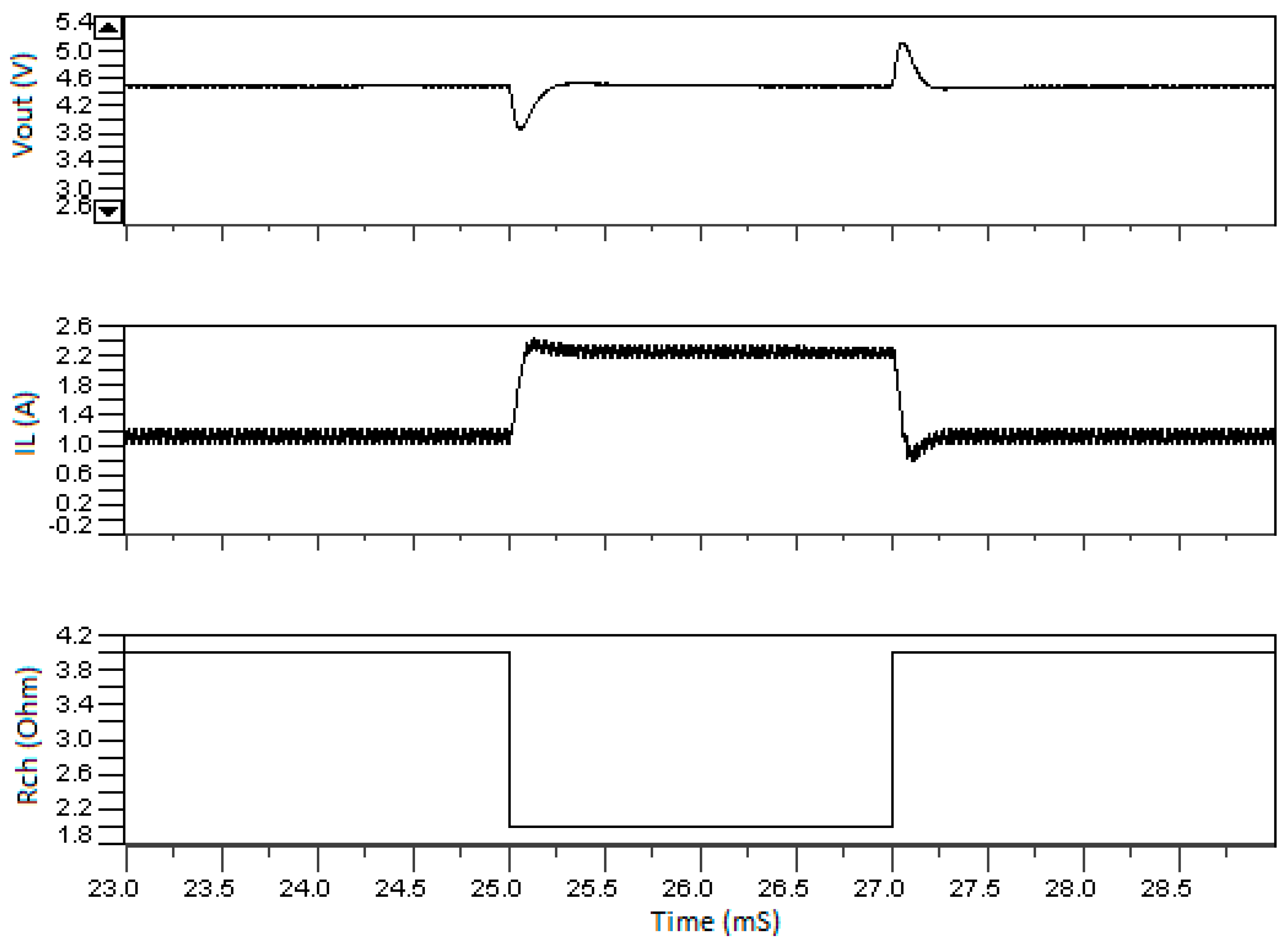
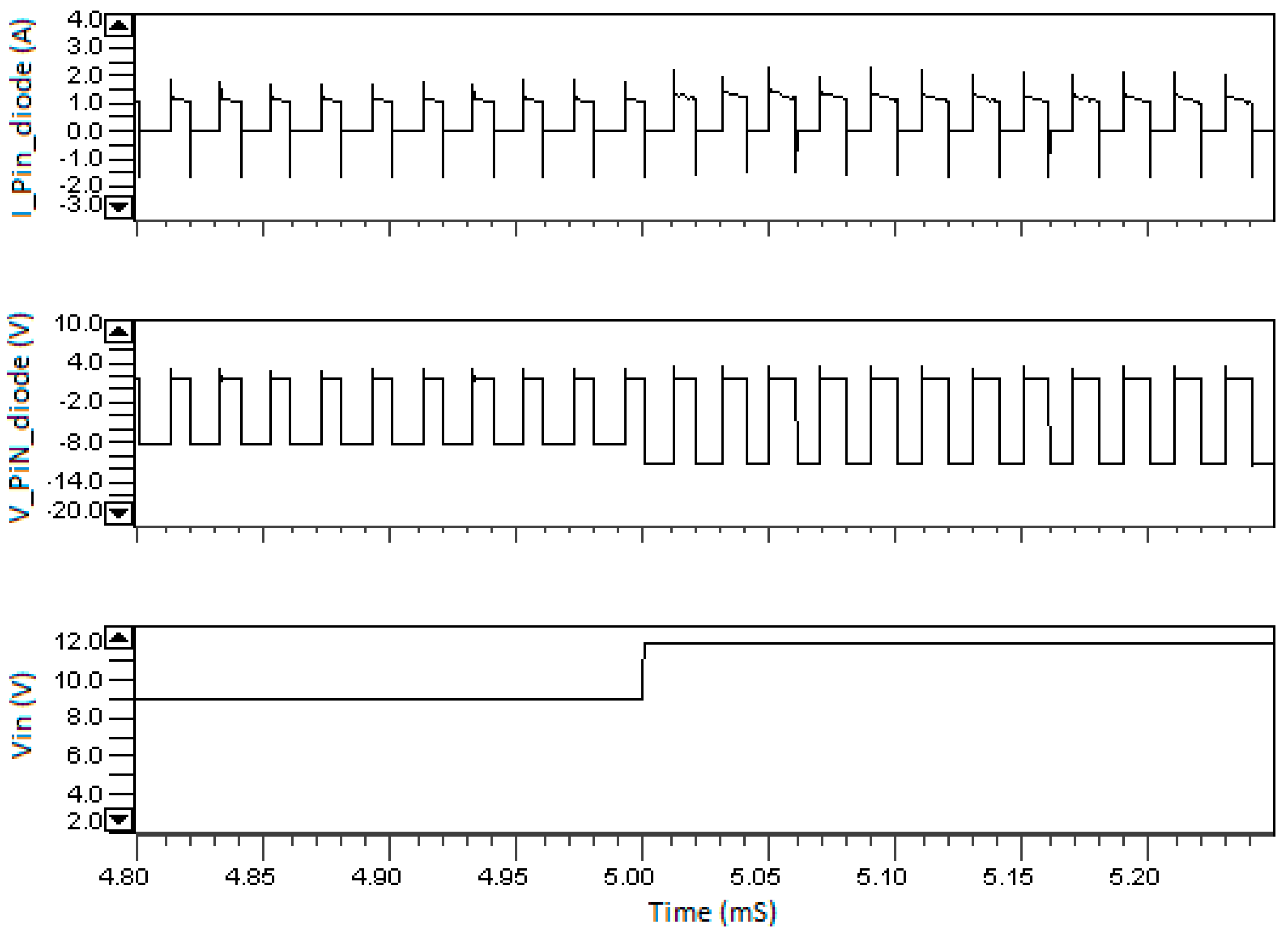
The simulation results of the bond graph buck model are displayed in Figure 11, Figure 12 and Figure 13. To show the output voltage regulation, we perturbed the input voltage (Figure 11) and the resistive charge (Figure 12) at various times during the simulation. As a result of these perturbations, we can see that the output voltage is regulated to the reference voltage (4.5 V). In Figure 13, we can see the inverse current of the PiN diode during its reverse recovery. Therefore, the simulation results of the bond graph buck model present satisfactory switching operation results.
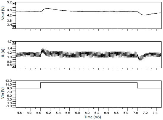
Figure 11.
Time evolution of the output voltage Vout(t) and the inductor current IL(t) during the Vin(t) jump and drop with an amplitude of 3 V at t = 5 ms and t = 7 ms.
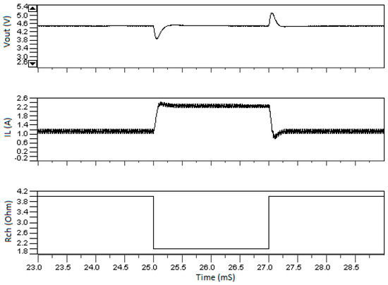
Figure 12.
Time evolution of the output voltage Vout(t) and the inductor current IL(t) during the R load drop and jump from 4 ohm to 2 ohm at t = 25 ms and back to 4 ohm at t = 27 ms.
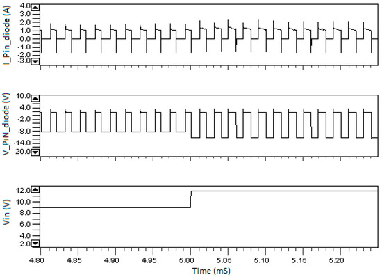
Figure 13.
Time evolution of the STTA81200 voltage and current during the Vin(t) jump with an amplitude of 3 V at t = 5 ms.
In addition, the bond graph buck model operates at the different switching modes without any modification on the model schema. Therefore, the use of a bond graph sub-model, based on the electrical components for the switcher devices, provides an unchanged causality of the buck bond graph schema for the different switching states. The commutation of the switcher devices is ensured mainly through the controlled flow element Ids for the power MOSFET IRF740 and the controlled flow elements Ij and Ib for the simple diode STTA81200.
5. Conclusions
In this paper, we present a methodology using the unified formalism of a bond graph to model a buck converter circuit. This approach allows us to model a bond graph buck converter very well at all switching modes. Thus, the use of a bond graph sub-model, based on the electrical elements for the switcher devices, allows for the maintenance of a causality invariant.
The design of the buck converter is realised using a bond graph package developed in the VHDL-AMS language and under the SystemVision environment. This is to achieve a rapid prototyping of the target design and to explore the graphics facility.
In future work, we will add the thermal effect within the switcher devices.
Acknowledgments
This work was supported by the Microelectronics and Instrumentation Laboratory.
Author Contributions
Rached Zrafi is the main author of the paper. Sami Ghedira and Kamel Besbes was responsible for the supervising of the paper.
Conflicts of Interest
The authors declare no conflict of interest.
References
- Borutzky, W. Bond Graph Methodology—Development and Analysis of Multidisciplinary Dynamic System Models; Springer: London, UK, 2010. [Google Scholar]
- Buisson, J.; Cormerais, H.; Richard, P.Y. Analysis of the bond graph model of hybrid physical systems with ideal switches. Proc. Inst. Mech. Eng. Part I 2002, 216, 47–63. [Google Scholar] [CrossRef]
- Borutzky, W. Bond Graph Model-Based Fault Diagnosis of Hybrid Systems; Springer: Cham, Switzerland; Heidelberg, Germany, 2015. [Google Scholar]
- Asher, G.M. The robust modelling of variable topology circuits using bond graphs. In Proceedings of the International Conference on Bond Graph Modelling (ICBGM’93), La Jolla, CA, USA, 17–20 January 1993. [Google Scholar]
- Umarikar, A.C.; Umanand, L. Modelling of switching systems in bond graphs using the concept of switched power junctions. J. Frankl. Inst. 2005, 342, 131–147. [Google Scholar] [CrossRef]
- Besbes, K. Modeling an insulated gate bipolar transistor using bond graph techniques. Int. J. Numer. Model. 1995, 8, 51–60. [Google Scholar] [CrossRef]
- Garrab, H.; Allard, B.; Morel, H.; Ghedira, S.; Besbes, K. Role of the temperature distribution on the pn junction behavior in the electro-thermal simulation. Int. J. Numer. Model. 2004, 17, 539–560. [Google Scholar] [CrossRef]
- Morel, H.; Allard, B.; Ghedira, S.; Ammous, A. A bond graph model of the PN junction. Simul. Ser. 1997, 29, 325–330. [Google Scholar]
- Alexander, H.S. Model Engineering in Mixed-Signal Circuit Design: A Guide to Generating Accurate Behavioral Models in VHDL-AMS; Springer: New York, NY, USA, 2001. [Google Scholar]
- Ashenden, P.J.; Peterson, G.D.; Teegarden, D.A. The System Designer’s Guide to VHDL-AMS: Analog, Mixed-Signal, and Mixed-Technology Modeling; Elsevier: Laguna Hills, CA, USA, 2003. [Google Scholar]
- Ibrahim, T. Contribution au Développement de Modèles Pour L’électronique de Puissance en VHDL-AMS. Ph.D. Dissertation, INSA-Lyon, Villeurbanne, France, 2009. [Google Scholar]
- Ma, C.L.; Lauritzen, P.O. A simple power diode model with forward and reverse recovery. IEEE Trans. Power Electron. 1993, 8, 342–346. [Google Scholar] [CrossRef]
- Borusky, W. Bond graphs and object oriented modeling—A comparison. Syst. Control. Eng. 2002, 216, 21–33. [Google Scholar]
- Maehne, T.; Vachoux, A.; Leblebici, Y. Development of a bond graph based model of computation for systemc-ams. In Proceedings of the IEEE Conference on PhD Research in Microelectronics and Electronics, Istanbul, Turkey, 22–25 June 2008. [Google Scholar]
- Pecheux, F.; Allard, B.; Lallement, C.; Vachoux, A.; Morel, H. Modeling and simulation of multi-discipline systems using bond graphs and VHDL-AMS. In Proceedings of the International Conference on Bond Graph Modeling and Simulation (ICBGM), New Orleans, LA, USA, 23–27 January 2005; pp. 149–155. [Google Scholar]
- Zrafi, R.; Ghedira, S.; Dhahri, Y.; Besbes, K. Simple VHDL-AMS PiN Diode Model Using Bond Graph Techniques. In Proceedings of the IEEE 16th International Conference on Sciences and Techniques of Automatic Control & Computer Engineering -STA’2015, Monastir, Tunisia, 21–23 December 2015; pp. 551–556. [Google Scholar]
- Zrafi, R.; Ghedira, S.; Dhahri, Y.; Besbes, K. Bond graph based automated modeling of switch-mode power converters using VHDL-AMS. In Proceedings of the IEEE International Conference on Control, Automation and Diagnosis (ICCAD), Hammamet, Tunisia, 19–21 January 2017. [Google Scholar]

© 2018 by the authors. Licensee MDPI, Basel, Switzerland. This article is an open access article distributed under the terms and conditions of the Creative Commons Attribution (CC BY) license (http://creativecommons.org/licenses/by/4.0/).