Article

A 1.93-pJ/Bit PCI Express Gen4 PHY Transmitter with On-Chip Supply Regulators in 28 nm CMOS

1
Department of Electrical Engineering and Computer Sciences, University of California at Berkeley, Berkeley, CA 94720, USA
2
Ayar Labs, Santa Clara, CA 95054, USA
3
Samsung Electronics, Hwaseong 445-330, Korea
4
Department of Electrical and Computer Engineering, Seoul National University, Seoul 08826, Korea
5
Inter-University Semiconductor Research Center, College of Engineering, Seoul National University, Seoul 08826, Korea
*
Author to whom correspondence should be addressed.
Woorham Bae and Sung-Yong Cho contributed equally to this work.
Electronics 2021, 10(1), 68; https://doi.org/10.3390/electronics10010068
Submission received: 11 December 2020 / Revised: 30 December 2020 / Accepted: 31 December 2020 / Published: 2 January 2021
(This article belongs to the Special Issue Mixed-Signal VLSI Design)

Abstract

:
This paper presents a fully integrated Peripheral Component Interconnect (PCI) Express (PCIe) Gen4 physical layer (PHY) transmitter. The prototype chip is fabricated in a 28 nm low-power CMOS process, and the active area of the proposed transmitter is 0.23 mm2. To enable voltage scaling across wide operating rates from 2.5 Gb/s to 16 Gb/s, two on-chip supply regulators are included in the transmitter. At the same time, the regulators maintain the output impedance of the transmitter to meet the return loss specification of the PCIe, by including replica segments of the output driver and reference resistance in the regulator loop. A three-tap finite-impulse-response (FIR) equalization is implemented and, therefore, the transmitter provides more than 9.5 dB equalization which is required in the PCIe specification. At 16 Gb/s, the prototype chip achieves energy efficiency of 1.93 pJ/bit including all the interface, bias, and built-in self-test circuits.

1. Introduction

Because Peripheral Component Interconnect Express (PCIe) is one of the most fast-evolving high-speed interface standards (for example the per-pin data rate is doubled every 4 years [1]), there are a lot of design challenges to meet PCIe Gen4 physical layer (PHY) transmitter specification. The challenges can be summarized as follows: at first, the maximum data rate increases to 16 Gb/s, while that of the prior PCIe Gen3 is 8 Gb/s. Moreover, because PCIe is required to provide backward compatibility, a PCIe Gen4 transmitter should also cover a lower data rates of 2.5 Gb/s (Gen1), 5 Gb/s (Gen2), and 8 Gb/s (Gen3) [1]. Secondly, it is required to implement a three-tap finite-impulse-response (FIR) equalization which include a pre-cursor and a post-cursor, while the equalization coefficients must be controllable, to suppress intersymbol interference (ISI) from variable channel loss. Thirdly, transmitter output impedance should be matched well as specified in return loss requirement, to minimize reflections for better signal integrity. Lastly, the output voltage swing should be adjustable.
In addition to the above essential requirements, supply voltage scalability is another key knob for improving energy efficiency across such wide data rates [1,2,3,4,5,6,7,8,9,10,11,12,13,14]. Ideally, the energy efficiency is expected to be flat across the data rate [6], which is rarely achieved in conventional fixed-voltage designs. Figure 1a shows an example of energy efficiency of the fixed-voltage design. The energy consumption is categorized with static current consumption, dynamic switching energy consumption, and signaling power over lossy transmission line [15,16]. At a lower data rate, the energy consumption by the signaling and the static current becomes less efficient because a fixed power is consumed regardless of the data rate. On the hand, the dynamic switching energy is fixed to CV2, regardless of the data rate. As a result, the overall energy efficiency is worse at a low data rate [17]. The signaling energy increases at a high data rate due to equalization power. On the other hand, the supply scaling allows improving the energy efficiency at a low data rate, as shown in Figure 1b, where a linear voltage–frequency scaling is assumed [17]. Because the contribution from the dynamic switching is significantly reduced at a low data rate, the energy efficiency curve becomes flatter compared to Figure 1a, in addition to the improved energy efficiency. Moreover, the supply scaling becomes more attractive in recent CMOS process technology where the circuits can take advantage of robust low-voltage operation [18]. This work presents design techniques for PCIe Gen4 transmitter and fabrication results in a 28 nm CMOS, which offers the supply-voltage scalability, as well as all the requirements of PCIe Gen4.
This paper is organized as follows: Section 2 describes the overall architecture and the details of circuit implementation for the proposed transmitter. In Section 3, the fabrication results from the prototype chip are discussed. Lastly, Section 4 concludes this paper.

2. Implementation of the Proposed PCIe Gen4 Transmitter

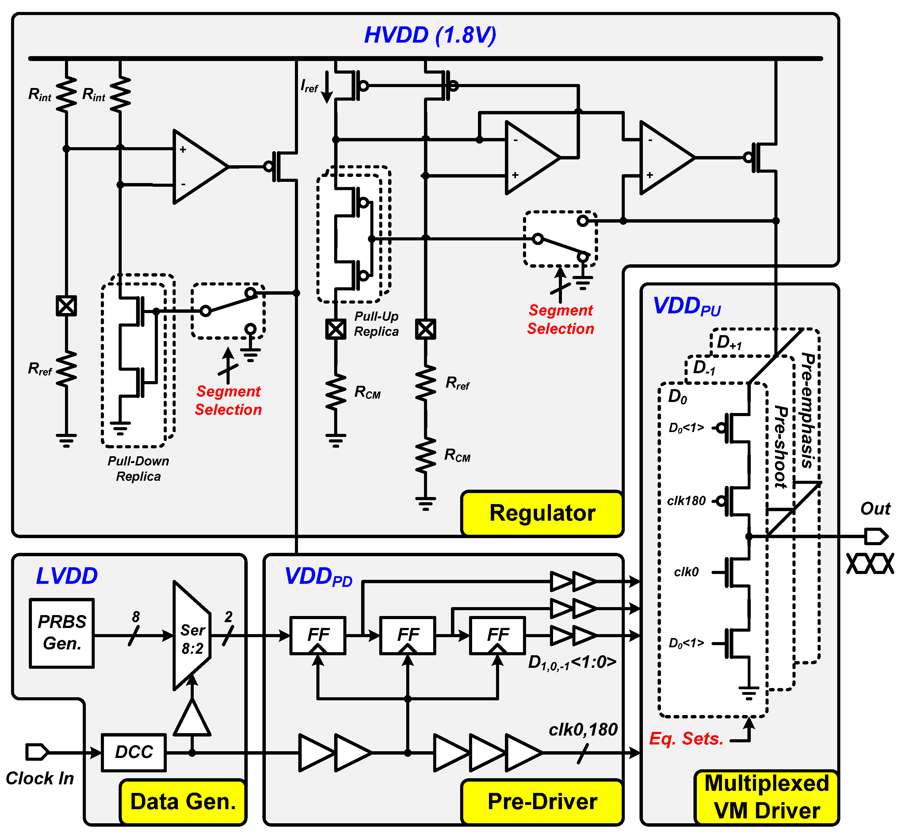
Figure 2 shows an overall architecture of the proposed PCIe Gen4 transmitter, which is fabricated in a 28 nm low-power CMOS process. In order to support the wide bitrate range without power penalty, a CMOS logic-based circuit topology and a scalable supply voltage using an on-chip regulator are employed; hence, a configurable voltage scaling is implemented in the proposed transmitter [19]. Considering the fanout-of-four (FO4) inverter delay across the process, voltage, and temperature (PVT) corners in the 28 nm CMOS technology, a half-rate clocking structure and a time-multiplexing driver are chosen to relax the required circuit bandwidth [12]. P-over-N source-series terminated (SST) or voltage-mode (VM) driver topology with stacked NMOS and PMOS is adopted to implement the time-multiplexing driver. Because the final 2:1 multiplexing happens at the very end of the transmitter, no ultra-high-speed (>8 Gb/s) circuit is used; hence, substantial power saving is achieved. In addition, the transistor stacking relaxes the electrostatic discharge (ESD) requirement due to CMOS snapback breakdown [20,21]. Compared to triple-stack topology with a quarter-rate clock [12], the double-stack allows less charge sharing and eases the overhead of multi-phase generation.
An eight-way parallel data stream is generated from the on-chip pseudo-random binary sequence-7 (PRBS-7) generator. Subsequently, the parallel data are serialized to a two-way stream by half-rate clock. The half-rate clock is externally provided and internally distributed using CMOS buffers. An open-loop duty-cycle corrector (DCC) based on an AC-coupled trans-impedance amplifier (TIA) is used to correct the duty-cycle distortion of the incoming clock [22,23,24]. The PRBS generator and the serializer are under a separate digital supply (LVDD) domain, to decouple the digital switching noise from the analog circuits.
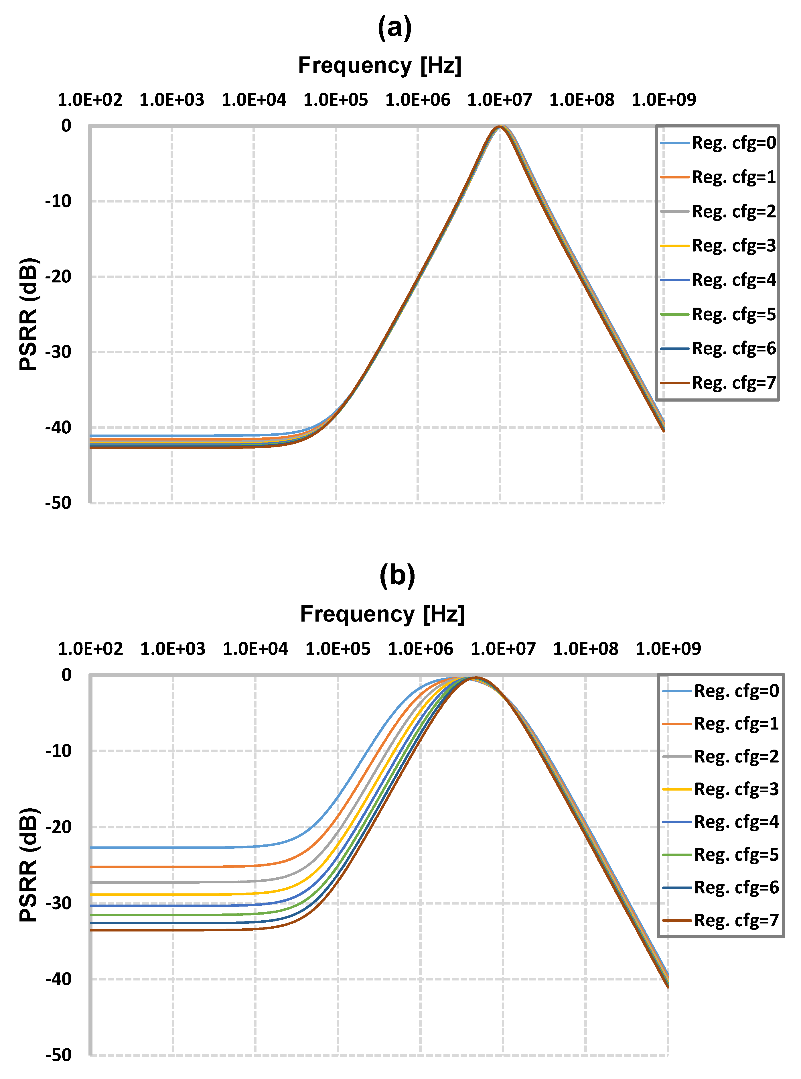
In the pre-driver stage, high-speed custom flip-flops are used to synchronize the 6 bit half-rate data stream for three-tap FIR equalization (D1<1:0>, D0<1:0>, D-1<1:0>) from the serialized stream. This also includes the data and clock buffers which drive large transistors of the time-multiplexing output drive, where the P-over-N SST topology provides the high output swing of PCIe Gen4 specification (>800 mV) with reasonable linearity (return loss < −10 dB) [25]. The pre-driver and the output driver are under the regulated supply voltages, VDDPU and VDDPD, respectively, which are configurable. Two supply regulators are dedicated to generating VDDPU and VDDPD from the 1.8 V supply (HVDD), which are used to match the output impedance of the transmitter, as well as to configure the voltage scaling and the output swing. The 1.8 V supply can be further reduced depending on the link requirements. Replica slices (pull-down path in the VDDPD regulator, pull-up path in the VDDPU regulator) of the output driver are used in the regulators to capture the impedance information of the actual output driver. Both the output driver and the replicas are segmented; therefore, the number of active segments becomes configurable. Because the regulators basically equalize the impedance of the replicas with the reference resistance by adjusting the regulated voltage, configuring the number of active segments achieves on-chip supply scaling. Specifically, because of its inverter-like structure, the P-over-N SST driver does not allow the pull-up (PMOS) and pull-down (NMOS) branches be turned on simultaneously. As a result, the pull-up and pull-down impedances can be controlled independently. Assuming linear operation, the impedance is a dominant function of gate-overdrive voltage, which is VDDPU-VT,P or VDDPD-VT,N, respectively, for pull-up and pull-down paths. Therefore, changing the number of active segments in the replica array lets the regulators adjust the VDDPU and VDDPD accordingly to match the impedance of the replica array and the reference resistance. For example, once the number of active segments is reduced, the regulator raises the supply voltage to increase the resistance per segment, to keep the same overall resistance. Therefore, the driver provides a stable output impedance regardless of the driver configuration, as [12] validates that the impedance variation is less than 10% of the target impedance. The segmentation of the output driver also enables the transmitter to configure FIR coefficients, by adjusting the number of segments belonging to the pre-cursor, main, and post-cursor taps. The driver segment selection (NAND and NOR gates) is placed at the first stage of the pre-driver to minimize redundant switching power due to data transition [12]. On the other hand, the replica segment selection is simply realized by connecting the gate to the regulated supply voltage or ground voltage without considering the data transition; as a result, a simple inverter in the regulated supply domain serves as the segment selection. For both regulators, simple one-stage differential amplifiers are used as the operational transconductance amplifiers. The dominant pole is placed at the gate of the pass transistor for both regulators, to stabilize the negative feedback loop with a reasonable size of the stabilizing capacitor which is placed at the output of the amplifier. The simulated power-supply rejection ratios (PSRR) of both regulators are shown in Figure 3. Because the dominant pole is placed at the gate of the pass transistor, a zero is introduced in the PSRR curve [26]. This is acceptable for this work, where the primary role of the regulators is to control the impedance, whereas the PSRR is a secondary benefit. In addition, the dominant pole is placed at a low enough frequency across all configurations (i.e., at least 10× lower frequency over the second pole), which confirms that the loop is stable regardless of the configurations.

3. Measurement Results

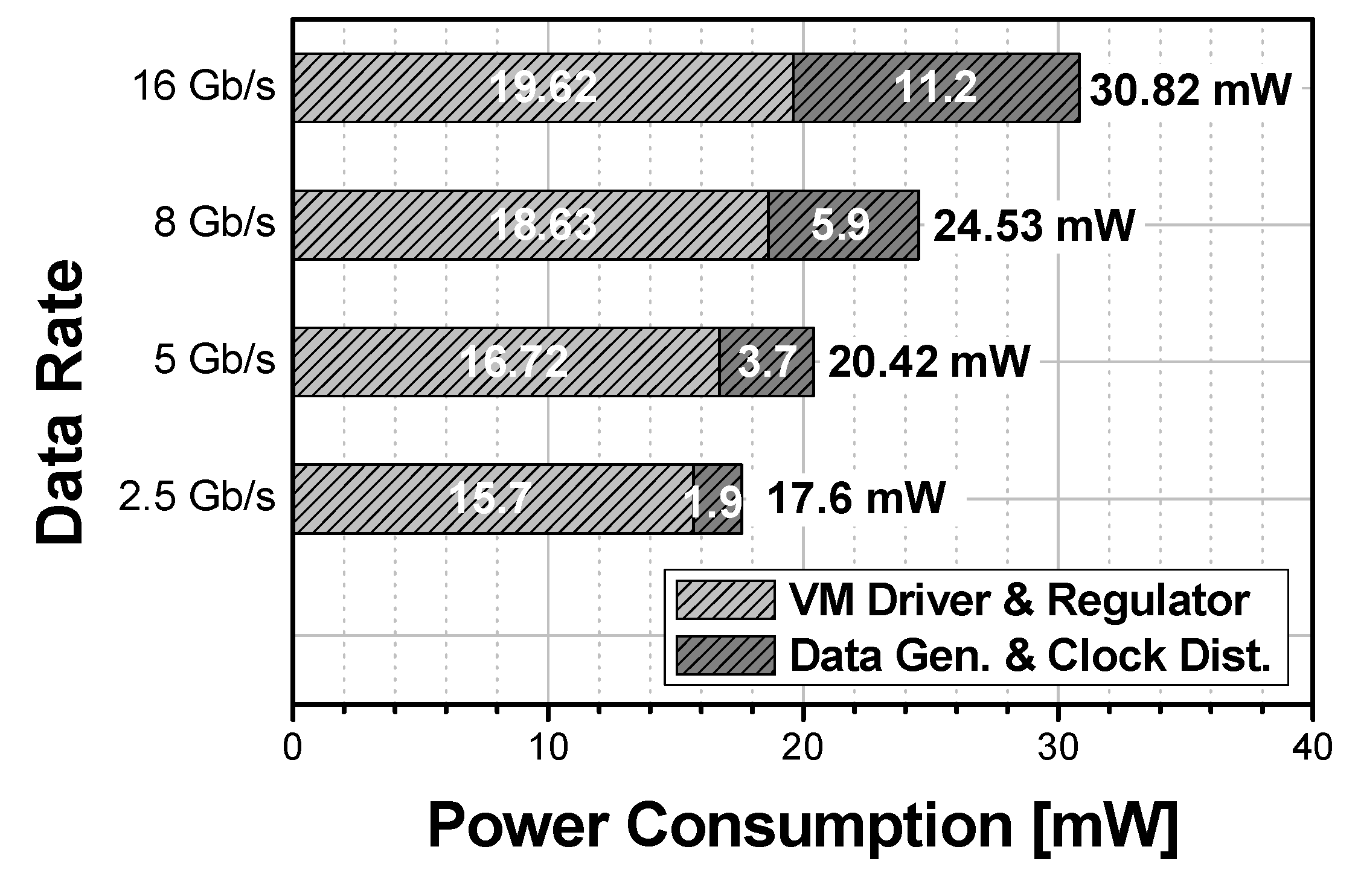
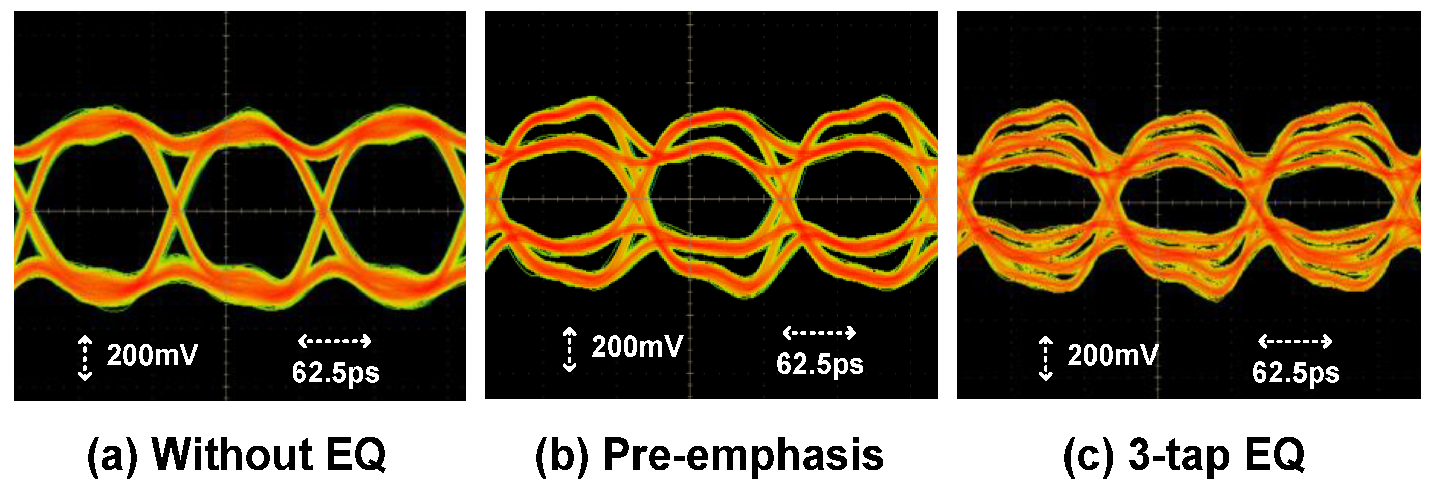
The proposed PCIe Gen4 transmitter is fabricated in a 28 nm low-power CMOS technology and occupies an active area of 0.023 mm2, while the full chip occupies 1 mm2. The chip photomicrograph and block description are shown in Figure 4. The prototype chip is wire-bonded on the test printed circuit board (PCB). The transmitter dissipates 30.8 mW at 16 Gb/s including all the interface buffers, bias circuits, and built-in self-test circuitry. Figure 5 shows the power breakdown at various data rates with nominal supply voltage and output swing configuration. Owing to the CMOS-based circuit implementation, the power consumption by the data generation, data buffers, and clock distribution is almost linearly scaled with the data rate. On the other hand, the power consumption of the output SST driver and the regulators is not scaled because they belong to the signaling and static power categories in Figure 1. However, this can be improved by lowering HVDD as the regulator headroom requirement is relaxed at a lower data rate. Figure 6 shows the measured eye diagrams at 8 Gb/s data rate with a low-loss channel, with respect to the three-tap FIR configuration, which verifies the proper operation of three-tap FIR equalization.
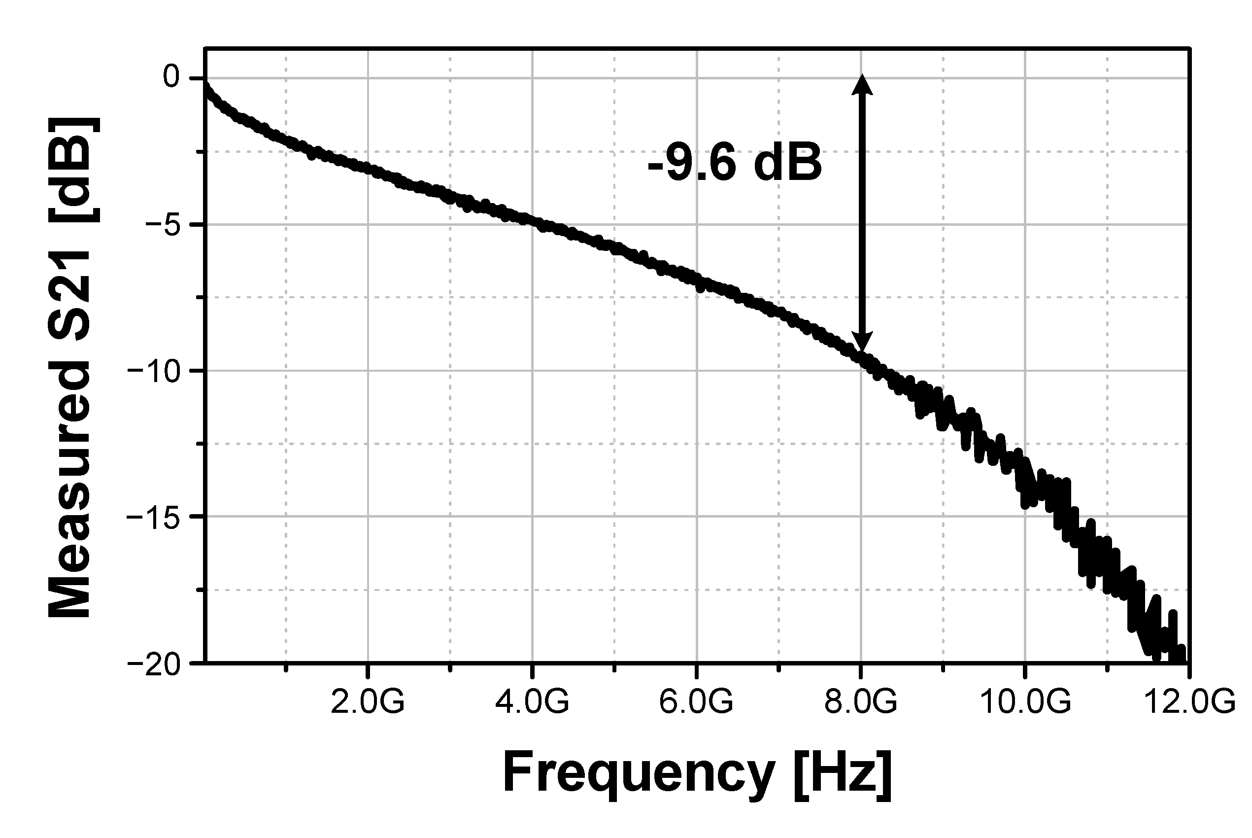
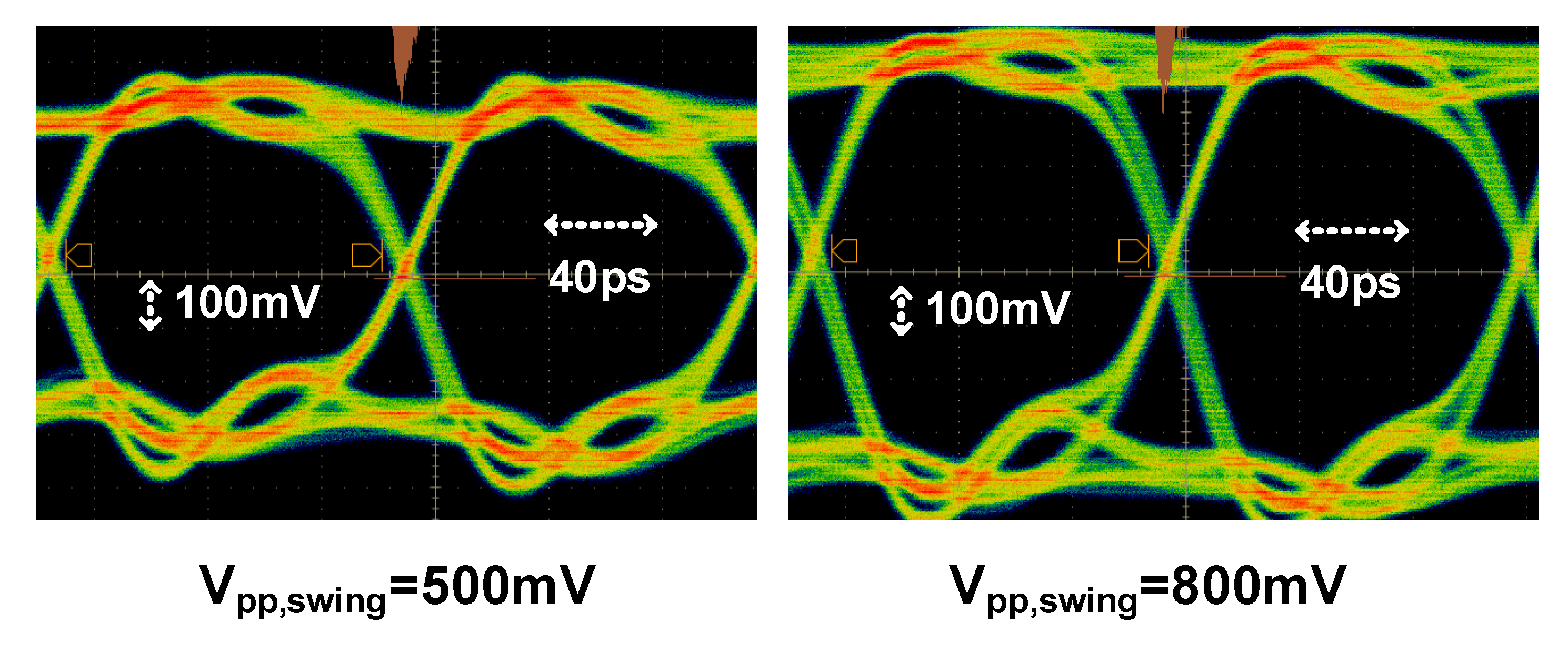
Because the supply regulators provide background calibration of the output impedance, the transmitter provides constant output impedance regardless of the FIR configuration; hence, the measured return loss of the prototype transmitter chip is less than −10 dB across all the frequencies of interest and passes the return loss specification of PCIe Gen4, as shown in Figure 7. In particular, the measured return loss at low frequency is less than −32 dB, which is equivalent to the impedance mismatch of less than 2.5 Ω, validating the impedance calibration method based on the supply regulators. In addition, as mentioned in the Section 2, the relaxed ESD requirement due to the stacked output driver improves the high-frequency return loss. A practical lossy channel is used to fully verify the effect of three-tap FIR equalization. Figure 8 and Figure 9 show the measured insertion loss (S21) of the lossy channel and the eye diagrams at 16 Gb/s with the lossy channel, respectively. With 9.6 dB channel loss at the Nyquist frequency (8 GHz), no residual ISI is found from the eye diagram with three-tap FIR equalization, which verifies that the proposed transmitter provides a sufficient compensation at Nyquist frequency larger than 9.5 dB, which is required from the PCIe Gen4 specification. In addition, we observe that the three-tap FIR equalizer gives a better eye opening compared to two-tap configuration, which justifies the implementation of the three-tap FIR. Figure 10 shows the output voltage swing measured with a Tektronix P7313 differential SMA probe module. The transmitter achieves the output swing of 800 mVpeak-to-peak,differential.
The performance of the fabricated transmitter is summarized and compared to other supply-scalable, wide-range transmitters in Table 1. Compared to the reference designs, the proposed transmitter achieves the best energy efficiency except for [13]. However, on-chip supply scaling is missing in [13]; consequently, it does not reflect the power overhead of on-chip supply scaling, such as the voltage dropout by a linear regulator or finite efficiency and switching noise of a switching regulator. As a result, considering that a substantial portion of the power is dissipated by the dropout of regulators, we can conclude that the proposed transmitter achieves the best efficiency among the supply-scalable transmitters.

4. Conclusions

A PCIe Gen4 PHY transmitter fabricated in a 28 nm CMOS was presented. The transmitter adopts supply voltage scaling to improve energy efficiency across a wide range using the on-chip supply regulators. The fabricated chip satisfies all the specifications of PCIe Gen4, including data rates, output swing, equalization, and return loss. The transmitter consumes 30.8 mW at 16 Gb/s and occupies an active area of 0.023 mm2.

Author Contributions

W.B. proposed and constructed the transmitter architecture. S.-Y.C. designed the transmitter in the 28 nm CMOS technology. D.-K.J. supervised and approved the project and the manuscript. All authors read and agreed to the published version of the manuscript.

Funding

This research received no external funding.

Institutional Review Board Statement

Not applicable.

Informed Consent Statement

Not applicable.

Data Availability Statement

Data is contained within the article or supplementary material.

Acknowledgments

The authors would like to thank Samsung Electronics for chip fabrication.

Conflicts of Interest

The authors declare no conflict of interest.

References

  1. Daly, D.C.; Fujino, L.C.; Smith, K.C. Through the Looking Glass-The 2018 Edition: Trends in Solid-State Circuits from the 65th ISSCC. IEEE Solid State Circuits Mag. 2018, 10, 30–46. [Google Scholar] [CrossRef]
  2. Li, S.; Spagna, F.; Chen, J.; Wang, X.; Tong, L.; Gowder, S.; Jia, W.; Lyer, S.; Song, R.; Li, L.; et al. A Power and Area Efficient 2.5–16 Gbps Gen4 PCIe PHY in 10 nm FinFET CMOS. In Proceedings of the 2018 IEEE Asian Solid-State Circuits Conference (A-SSCC), Tainan, Taiwan, 5–7 November 2018; pp. 5–8. [Google Scholar]
  3. Shang, L.; Peh, L.-S.; Jha, N.K. Dynamic Voltage Scaling with Links for Power Optimization of Interconnection Networks. In Proceedings of the International Symposium on High.-Performance Computer Architecture (HPCA), Anaheim, CA, USA, 12 February 2003; pp. 91–102. [Google Scholar]
  4. Shin, D.; Kim, J. Power-Aware Communication Optimization for Networks-On-Chips with Voltage Scalable Links. In Proceedings of the IEEE/ACM/IFIP International Conference on Hardware/Software Codesign and System Synthesis, Stockholm, Sweden, 8–10 September 2004; pp. 170–175. [Google Scholar]
  5. Barroso, L.A.; Hölzle, U. The Case for Energy-Proportional Computing. Computer 2007, 40, 33–37. [Google Scholar] [CrossRef]
  6. Abts, D.; Marty, M.R.; Wells, P.M.; Klausler, P.; Liu, H. Energy Proportional Datacenter Networks. In Proceedings of the International Symposium on Computer Architecture (ISCA), Saint Malo, France, 19–23 June 2010; pp. 338–347. [Google Scholar]
  7. Shu, G.; Choi, W.; Saxena, S.; Kim, S.; Talegaonkar, M.; Nandwana, R.; Wei, D.; Nandi, T. A 16Mb/s-to-8Gb/s 14.1-to-5.9pJ/b Source Synchronous Transceiver Using DVFS and Rapid On/Off in 65 nm CMOS. In Proceedings of the 2016 IEEE International Solid-State Circuits Conference (ISSCC), San Francisco, CA, USA, 31 January–4 February 2016; pp. 398–399. [Google Scholar]
  8. Ramachandran, A.; Anand, T. A 0.5-to-0.9V, 3-to-16Gb/s, 1.6-to-3.1pJ/b Wireline Transceiver Equalizing 27dB Loss at 10Gb/s with Clock-Domain Encoding Using Integrated Pulse-Width Modulation (iPWM) in 65nm CMOS. In Proceedings of the 2018 IEEE International Solid-State Circuits Conference-(ISSCC), San Francisco, CA, USA, 11–15 February 2018; pp. 268–269. [Google Scholar]
  9. Wei, G.-Y.; Kim, J.; Liu, D.; Sidiropoulos, S.; Horowitz, M.A. A variable-frequency parallel I/O interface with adaptive power-supply regulation. IEEE J. Solid State Circuits 2000, 35, 1600–1610. [Google Scholar]
  10. Kim, J.; Horowitz, M.A. Adaptive supply serial links with sub-1-V operation and per-pin clock recovery. IEEE J. Solid State Circuits 2002, 37, 1403–1413. [Google Scholar] [CrossRef]
  11. Balamurugan, G.; Kennedy, J.; Banerjee, G.; Jaussi, J.E.; Mansuri, M. A scalable 5-15 Gbps, 14-75 mW low-power I/O transceiver in 65 nm CMOS. IEEE J. Solid State Circuits 2008, 43, 1010–1019. [Google Scholar] [CrossRef]
  12. Bae, W.; Ju, H.; Park, K.; Han, J.; Jeong, D. A Supply-Scalable Serializing Transmitter with Controllable Output Swing and Equalization for Next Generation Standards. IEEE Trans. Ind. Electron. 2018, 65, 5979–5989. [Google Scholar] [CrossRef]
  13. Mansuri, M.; Jaussi, J.E.; Kennedy, J.T.; Hsueh, T.-C.; Shekhar, S.; Balamurugan, G.; Robarts, F.; Casper, P. A Scalable 0.128–1 Tb/s, 0.8–2.6 pJ/bit, 64-Lane Parallel I/O in 32-nm CMOS. IEEE J. Solid State Circuits 2013, 48, 3229–3242. [Google Scholar] [CrossRef]
  14. Chen, X.; Wei, G.; Peh, L.-S. Design of Low-Power Short-Distance Opto-Electronic Transceiver Front-Ends with Scalable Supply Voltages and Frequencies. In Proceedings of the 2008 International Symposium on Low Power Electronics & Design, Bangalore, India, 11–13 August 2008; pp. 277–282. [Google Scholar]
  15. Chang, K.-Y.K.; Wei, J.; Huang, C.; Li, S.; Donnelly, K.; Horowitz, M.; Li, Y.; Sidiropoulos, S. A 0.4–4-Gb/s CMOS Quad Transceiver Cell Using On-Chip Regulated Dual-Loop PLLs. IEEE J. Solid State Circuits 2003, 38, 747–754. [Google Scholar] [CrossRef]
  16. Eble, J.C.; Best, S.; Leibowitz, B.; Luo, L.; Palmer, R.; Wilson, J.; Zerbe, J.; Amirkhany, A.; Nguyen, N. Power-Efficient I/O Design Considerations for High-Bandwidth Applications. In Proceedings of the IEEE Custom Integrated Circuits Conference, San Jose, CA, USA, 19–21 September 2011; pp. 1–4. [Google Scholar]
  17. Bae, W. Supply-Scalable High-Speed I/O Interfaces. Electronics 2020, 9, 1315. [Google Scholar] [CrossRef]
  18. Bohr, M.T.; Young, I.A. CMOS Scaling Trends and Beyond. IEEE Mirco 2017, 37, 20–29. [Google Scholar] [CrossRef]
  19. Chen, S.; Zhou, L.; Zhuang, I.; Im, J.; Melek, D.; Namkoong, J.; Raj, M.; Shin, J.; Frans, Y.; Chang, K. A 4-to-16 GHz inverter-based injection-locked quadrature clock generator with phase interpolators for multi-standard I/Os in 7 nm FinFET. In Proceedings of the 2018 IEEE International Solid-State Circuits Conference-(ISSCC), San Francisco, CA, USA, 11–15 February 2018; pp. 390–392. [Google Scholar]
  20. Ker, M.D. Whole-chip ESD protection design with efficient VDD-to-VSS ESD clamp circuits for submicron CMOS VLSI. IEEE Trans. Electron. Devices 1999, 46, 173–183. [Google Scholar]
  21. Vashchenko, V.A.; Scholz, M.; Jansen, P.; Peterson, R.; Natarajan, M.I.; Tremouilles, D.; Sawada, M.; Nakaei, T.; Hasebe, T.; Beek, T.; et al. Turn-off characteristics of the CMOS snapback ESD protection devices-new insights and its implications. In Proceedings of the 2006 Electrical Overstress/Electrostatic Discharge Symposium, Anaheim, CA, USA, 10–15 September 2006; pp. 39–45. [Google Scholar]
  22. Bae, W.; Ju, H.; Park, K.; Cho, S.; Jeong, D. A 7.6 mW, 414 fs RMS-Jitter 10 GHz Phase-Locked Loop for a 40 Gb/s Serial Link Transmitter Based on a Two-Stage Ring Oscillator in 65 nm CMOS. IEEE J. Solid State Circuits 2016, 51, 2357–2367. [Google Scholar] [CrossRef]
  23. Savoj, J.; An, F.; Gong, J.; Im, J.; Jiang, X.; Jose, A.; Kireev, V.; Lim, S.; Roldan, A.; Turker, D.Z.; et al. A Low-Power 0.5–6.6 Gb/s Wireline Transceiver Embedded in Low-Cost 28 nm FPGAs. IEEE J. Solid State Circuits 2013, 48, 2582–2594. [Google Scholar] [CrossRef]
  24. Bae, W. CMOS Inverter as Analog Circuit: An Overview. J. Low Power Electron. Appl. 2019, 9, 26. [Google Scholar] [CrossRef] [Green Version]
  25. Menolfi, C.; Toifl, T.; Buchmann, P.; Kossel, M.; Morf, T.; Weiss, J.; Schmatz, M. A 16Gb/s Source-Series Terminated Transmitter in 65nm CMOS SOI. In Proceedings of the 2007 IEEE International Solid-State Circuits Conference. Digest of Technical Papers, San Francisco, CA, USA, 11–15 February 2007; pp. 446–614. [Google Scholar]
  26. Bae, W.; Jeong, D.-K. Analysis and Design of CMOS Clocking Circuit for Low Phase Noise; Institute of Engineering and Technology: London, UK, 2020. [Google Scholar]
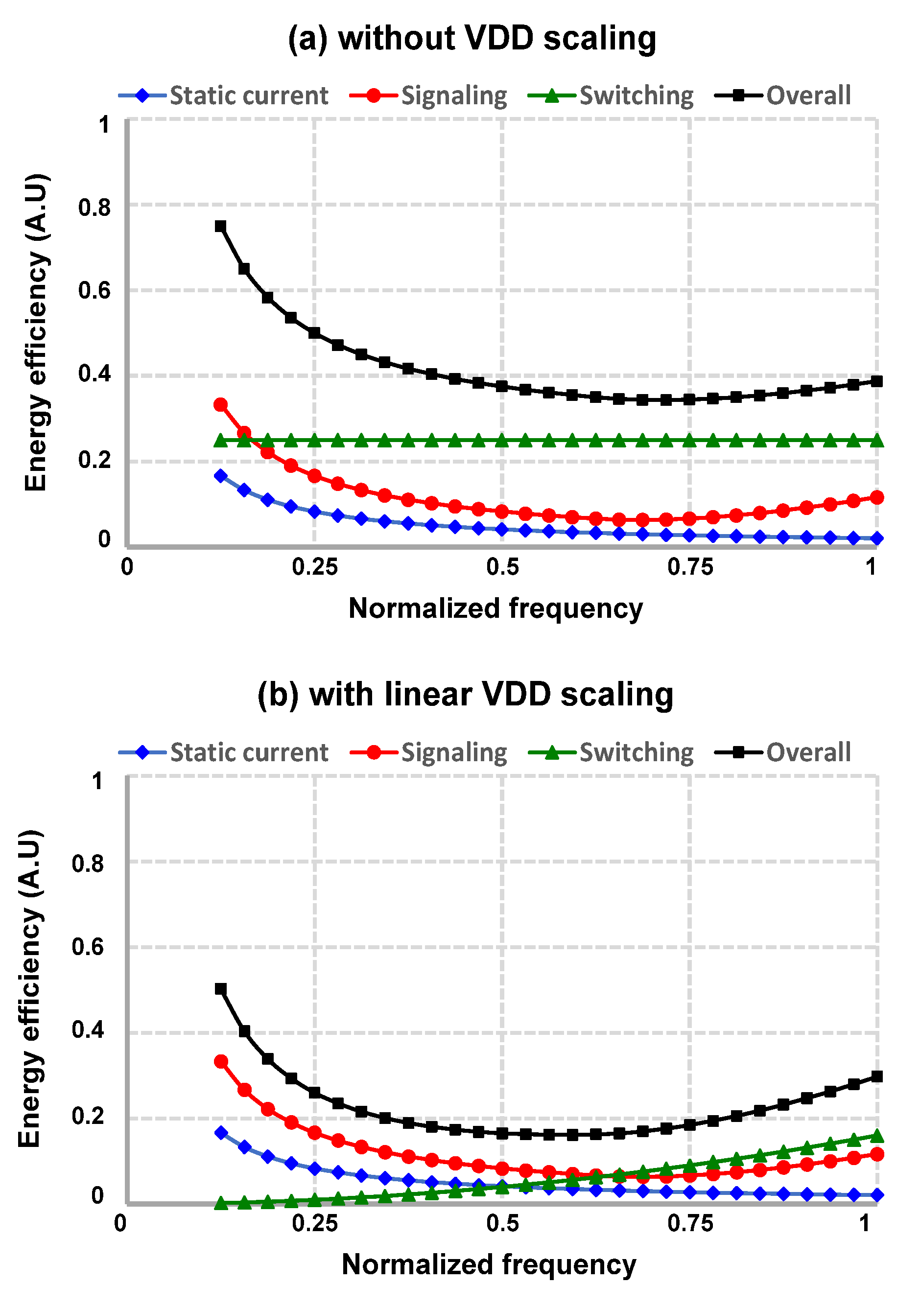
Figure 1. Theoretical energy efficiency breakdown of a physical layer (PHY) transmitter: (a) without supply scaling; (b) with supply scaling.
Electronics 10 00068 g001
Figure 2. Overall architecture of the proposed Peripheral Component Interconnect Express (PCIe) Gen4 transmitter.
Electronics 10 00068 g002
Figure 3. Simulated power-supply rejection ratio (PSRR) of (a) VDDPU regulator and (b) VDDPD regulator across regulator segment configuration.
Electronics 10 00068 g003
Figure 4. Die photomicrograph and block description.
Electronics 10 00068 g004
Figure 5. Measured power consumption and breakdown across data rate.
Electronics 10 00068 g005
Figure 6. Measured eye diagrams at 8 Gb/s with respect to finite-impulse-response (FIR) equalization tap configuration: (a) eye diagram without equalization; (b) eye diagram with only pre-emphasis equalization; (c) eye diagram with 3-tap equalization.
Electronics 10 00068 g006
Figure 7. Return loss specification of PCIe Gen4 transmitter and measured return loss from the prototype chip.
Electronics 10 00068 g007
Figure 8. Measured channel S21 characteristic.
Electronics 10 00068 g008
Figure 9. Measured eye diagram at 16 Gb/s with the lossy channel with respect to the FIR equalization tap configuration.
Electronics 10 00068 g009
Figure 10. Output differential swing measured with Tektronix P7313 differential SMA probe.
Electronics 10 00068 g010
Table 1. Performance comparison.
Process (nm)Min. Rate (Gb/s)Max. Rate (Gb/s)EqualizerClockingSupply ScalingMin. TX Swing (Vppd)Max. TX Swing (Vppd)Power (mW) @Max RateArea (mm2)FoM (pJ/bit) @Max Rate
[7]65383-tap FFE (feed-forward equalizer)Half rateDC–DC + regulatorN/AN/A38.4N/A4.8
[8]65316PWM (pulse-width modulation)Quarter rateExternal sourceN/AN/A38.78N/A2.42
[9]3500.20.8NoneHalf rateDC–DC0.10.1521.5N/A26.875
[10]2500.655None1/5 rateDC–DC0.10.3216.6N/A43.3
[11]655153-tap FFEHalf rateExternal source0.10.72340.0332.3
[12]655322-tap FFEQuarter rateOn-chip regulator0.41.387.70.172.74
[13]322163-tap FFEQuarter rateExternal source0.360.5250.0141.56
This work282.5163-tap FFEHalf rateOn-chip regulator0.50.830.820.0231.93
Publisher’s Note: MDPI stays neutral with regard to jurisdictional claims in published maps and institutional affiliations.