Article

Design and Implementation of RF Front-End Module Based on 3D Heterogenous-Integrated Wafer-Level Packaging

School of Aeronautics and Astronautics, Zhejiang University, Hangzhou 310027, China
*
Author to whom correspondence should be addressed.
Electronics 2021, 10(16), 1893; https://doi.org/10.3390/electronics10161893
Submission received: 16 June 2021 / Revised: 2 August 2021 / Accepted: 3 August 2021 / Published: 6 August 2021
(This article belongs to the Section Microelectronics)

Abstract

:
In this paper, a three-dimensional heterogenous-integrated (3DHI) wafer-level packaging (WLP) process is proposed, and a radio frequency (RF) front-end module with two independent ultra-high frequency (UHF) receiving channels are designed and implemented, which covers 400 MHz–600 MHz and 2050 MHz–2200 MHz respectively for unmanned aerial vehicle (UAV) applications. The module is formed by wafer-to-wafer (W2W) bonding of two high-resistivity silicon (HR-Si) interposers with embedded bare dies and through silicon via (TSV) interconnections. Double-sided deep reactive ion etching (DRIE) and conformal electroplating process are introduced to realize the high-aspect-ratio TSV connection within 290 µm-thick cap interposer. Co-plane waveguide (CPW) transmission lines are fabricated as the process control monitor (PCM), the measured insertion loss of which is less than 0.18 dB/mm at 35 GHz. The designed RF front-end module is fabricated and measured. The measured return loss and gain of each RF channel is better than 13 dB and 21 dB, and the noise figure is less than 1.5 dB. In order to evaluate the capability of the 3DHI process for multi-layer interposers, the module is re-designed and fabricated with four stacked high-resistivity silicon interposers. After W2W bonding of two pairs of interposers and wafer slicing, chip-to chip (C2C) bonding is applied to form a four-layer module with operable temperature gradient.

1. Introduction

The development of a highly integrated and high-performance RF module based on silicon technologies in recent decades has attracted more and more attention in modern communication systems. To deliver and receive data with different communication modes, multi RF channels are commonly integrated under one package, which increases the complexity and the size of communication systems.
In order to solve this problem, researchers focus on the attempts to integrate multi RF front-end devices into one compact module by using 3D packaging technology. Reference [1] introduces several multi-layer substrates which are commonly chosen for microwave or millimeter-wave 3D packaging process, like high temperature co-fired ceramic (HTCC) [2,3], low temperature co-fired ceramic (LTCC) [4,5,6], and organic substrate [7,8]. HTCC is often considered to be the lowest cost ceramic technology [9], but it suffers from a significant insertion loss due to the low conductivity of tungsten used as the metal of transmission, especially at mm-wave frequencies. LTCC shows remarkable RF performance from DC to 110 GHz. For example, Carlofelice et al [10] have provided an X-band 3D LTCC TR module for satellite phased-array radars, which is the first time 3D LTCC packaging is applied in space. The main drawback of 3D LTCC is its poor thermal conductivity [11]. This disadvantage also appears on organic substrates. Most importantly, all the processes face the same problems: RF chips can hardly be buried in substrate and stacked on profile direction because of the high temperature used in process flow (which may damage the embedded devices) and the large deviation of shrinking rates among substrate and chips.
However, HR-Si has a reasonable price, compared with ceramic and compound semiconductor. The TSVs and redistribution layers (RDLs) fabricated on HR-Si interposer has high dimensional resolution and extraordinary performance of vertical RF transmission. Furthermore, vertically stacked HR-Si interposers with embedded chips have more advantages in flexible heterogenous integrations than in the traditional heterostructure semiconductor process [12,13]. Moreover, the thermal conductivity of HR-Si is high, which is about one third of copper. Most of the thermal dissipation produced from embedded power devices can be easily transferred through substrate and TSVs [14].
In this paper, an HR-Si based 3DHI WLP process is proposed, and an UHF 3DHI front-end module which is used in unmanned aerial vehicle (UAV) system is presented. The operation frequency of the module covers both the radio location band (400 MHz–600 MHz) and the data transmission band (2050 MHz–2300 MHz). Two interposer-stacking structures are provided to realize the 3DHI module. One is formed by two stacked surface-passivated HR-Si interposers with embedded chips and through silicon via (TSV) interconnections. This multi-layer wafer is diced and measured; after that the cap wafer and bottom wafer with different type of TSVs are bonded. The other one has four stacked HR-Si interposers, for which two double-stacked interposers are diced and stacked again through low-temperature C2C bonding. Besides these, insertion loss and return loss of CPW are measured using the same process. The design and implementation details will be discussed in Section 2, Section 3 and Section 4.

2. Process Flow of the 3DHI WLP

In order to realize multi-layer vertical stacking of RF chips, a 3DHI WLP process with up to four stacked HR-Si interposers is designed and presented, the structural diagram of which is shown in Figure 1. The four-layer interposer structure with two-layer embedded RF chips can be divided into two assemblies; both assemblies are constructed with one 290 µm-thick cap interposer wafer and one 190 µm-thick bottom interposer wafer. These two wafers adopt different process flows due to different interposer thickness. The process of each interposer wafer and the assembly of the four-layer interposer structure will be discussed below in detail.

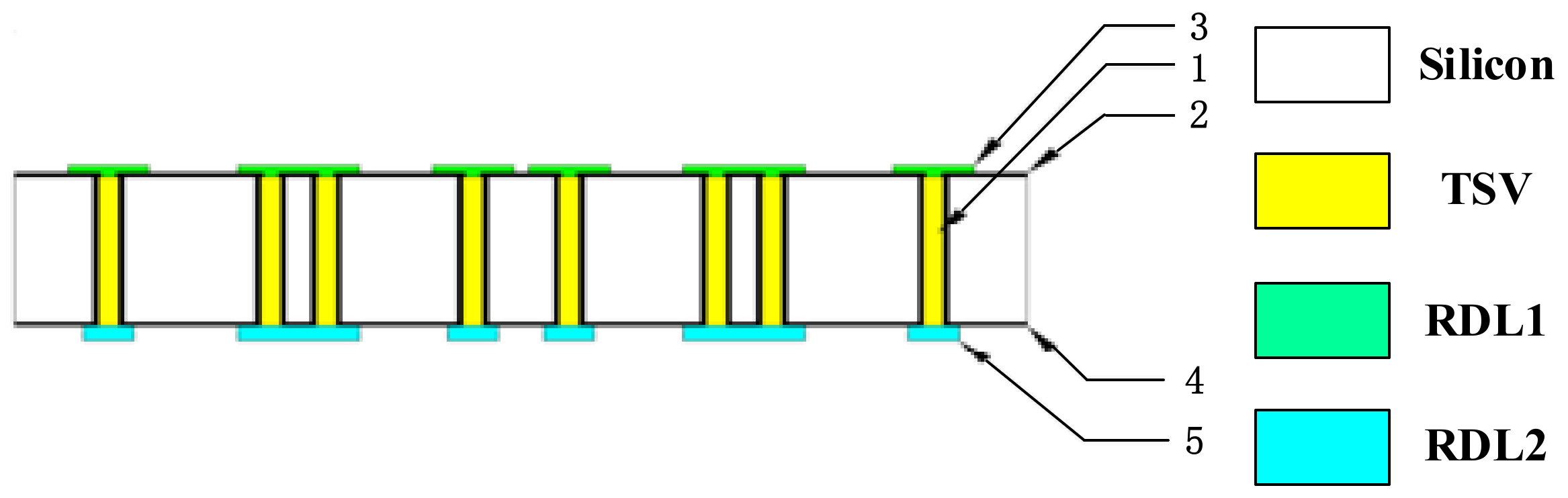
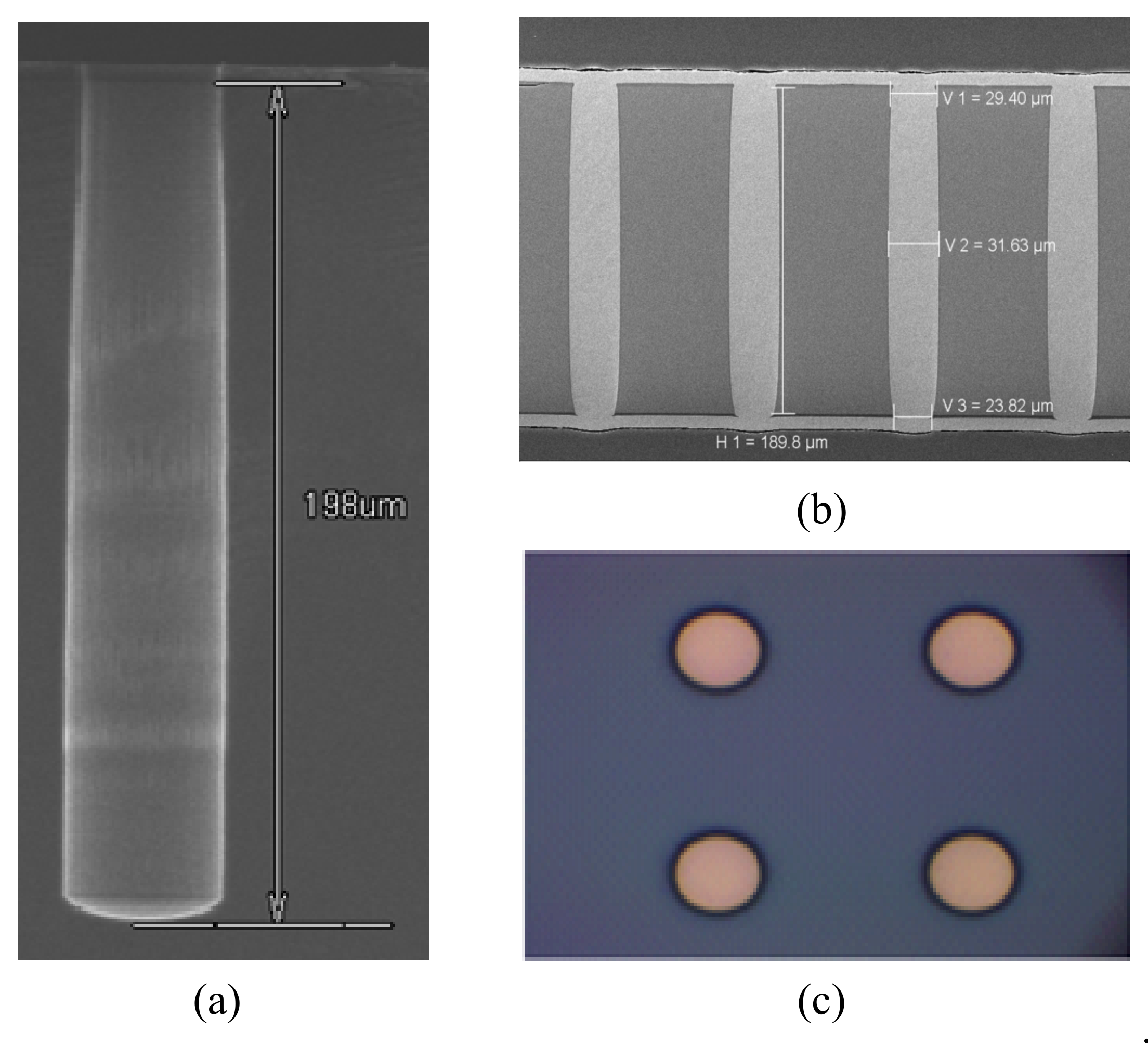
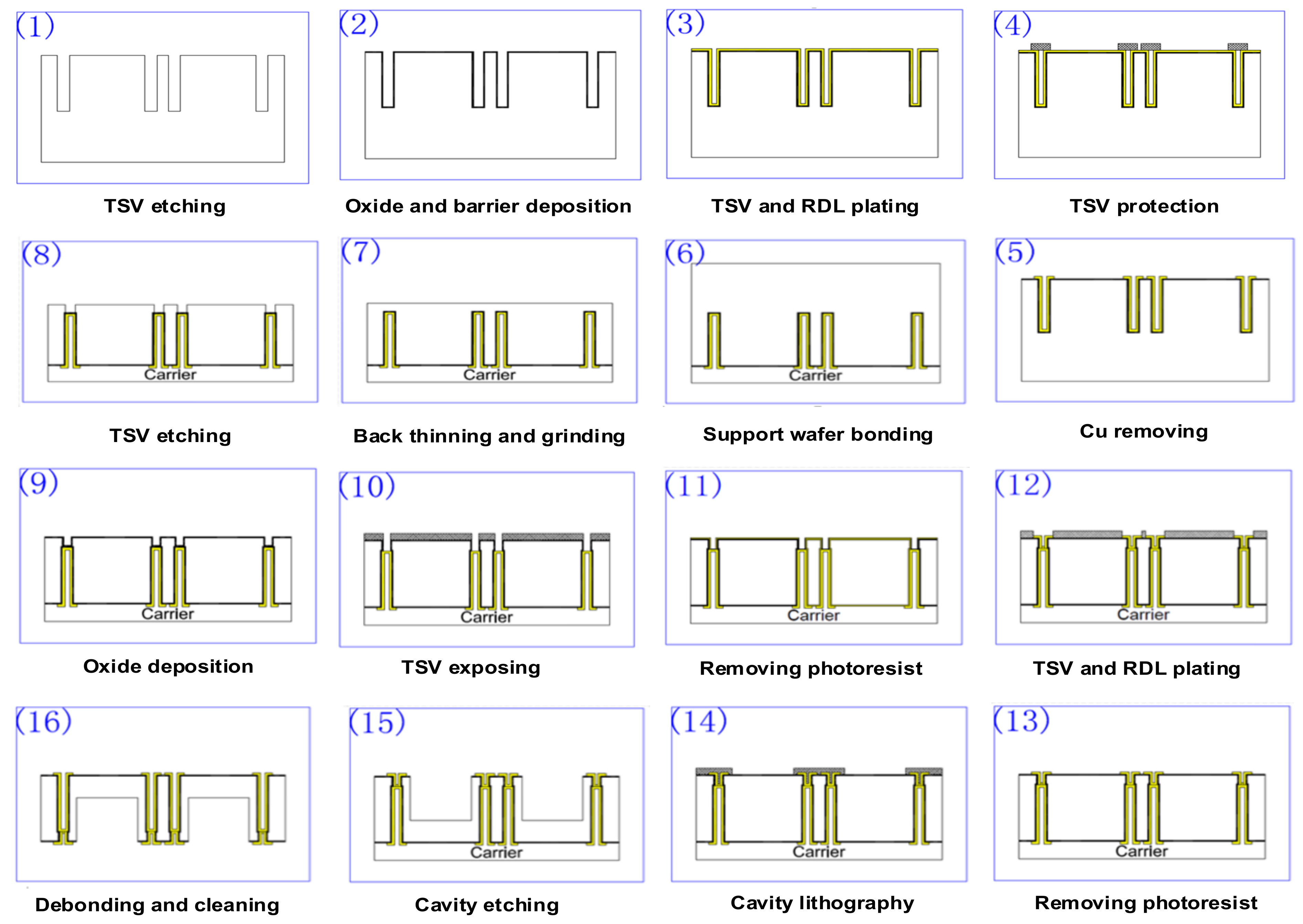
2.1. Process of the Bottom Interposer Wafer

Figure 2 shows the cross section of the bottom HR-Si interposer wafer with φ30 µm × 190 µm TSV and double-side re-distribution layer (RDL). The fabrication process flow is shown in Figure 3.
The raw 8-inch HR-Si wafers are 710-µm-thick with resistivity above 2000 Ω·cm. Based on Bosch process [15], interposer wafer fabrication starts with φ30 µm × 200 µm TSV etching from the front side by using deep reactive ion etching (DRIE). Secondly, TSVs are passivated with SiO2 and followed by Ti/Cu seed layer deposition. Thirdly, TSVs are completely filled with Cu by electroplating and the Cu layer on the front side surface is removed with chemical-mechanical polishing (CMP). After fabricating Cu RDL on the front side, chemical-plating of Ni/Pb/Au is applied on the Cu RDL to support latter wire bonding process. Fourthly, the front side of the interposer wafer is bonded with a support wafer by using temporary adhesive bonding [16]. Fifthly, TSVs are exposed from the backside of the interposer wafer with back-thinning and grinding to 190 µm thick, followed by PI deposition and TSV exposing. Finally, Cu RDL and Ni/Pb/Au plating are formed on the backside of interposer wafer, followed by support wafer debonding and wafer cleaning. The key fabrication parameters of the above process are given in Table 1.
The critical process of the bottom cap is the metal filling in the high-aspect-ratio TSVs. The common problems faced are unable to start electroplating or leaving voids after electroplating, especially in our TSV whose aspect ratio is larger than 6:1 with 30 µm diameter and 190 µm depth, which may lead to reliability, hermetic, and electrical issues. Therefore, the plating additives consisting of accelerator, suppressor, leveler, and other processing parameters, and also the plating current density and time, need to be considered carefully to achieve void-free full-via plating. The SEM of our TSVs is shown in Figure 4.

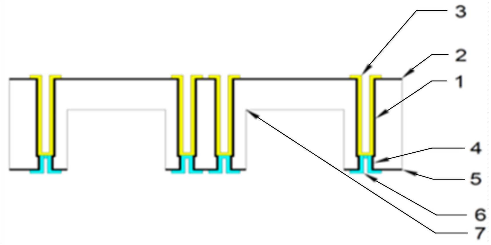
2.2. Process of the Cap Interposer Wafer

Commonly, the thickness of the embedded RF chips is 100 µm. After chips mounting on the bottom interposer, the height from the chip pads to the interposer is beyond 100 µm. To perform wire bonding between them, the height of a φ25 µm gold wire above the chip surface is about 80 µm. Therefore, a 290 µm-thick cap interposer wafer with 200 µm-deep cavities is desired to fulfill the chip embedding and ensure the mechanical strength during the latter W2W bonding process.
Double-side TSV process is presented to realize the ultra-thick silicon interposer. The cross section of the cap interposer wafer is shown in Figure 5. The fabrication process flow is shown in Figure 6.
The Bosch process is applied to etch the φ60 µm × 250 µm TSVs from the front side of a raw HR-Si wafer. Furthermore, the thick TSVs are filled by combing the conformal electroplating process and bottom-up electroplating process. After the front side process finished, the φ50 µm × 40 µm TSVs are etched from the backside with operable overlapping in the same location. The opening window on the insulating layer at the bottom of each front side TSV is completed by DRIE process. Then backside TSVs are filled by using the conformal electroplating. After the Cu/Ni/AgSn RDL plating, the 200 µm-deep cavity is etched from the backside. The thinnest cap structures produced so far had a thickness of 90 µm. Figure 7 shows the SEM images of the conformal-plated TSVs and the cavities. The key fabrication parameters of the above process are given in Table 2.

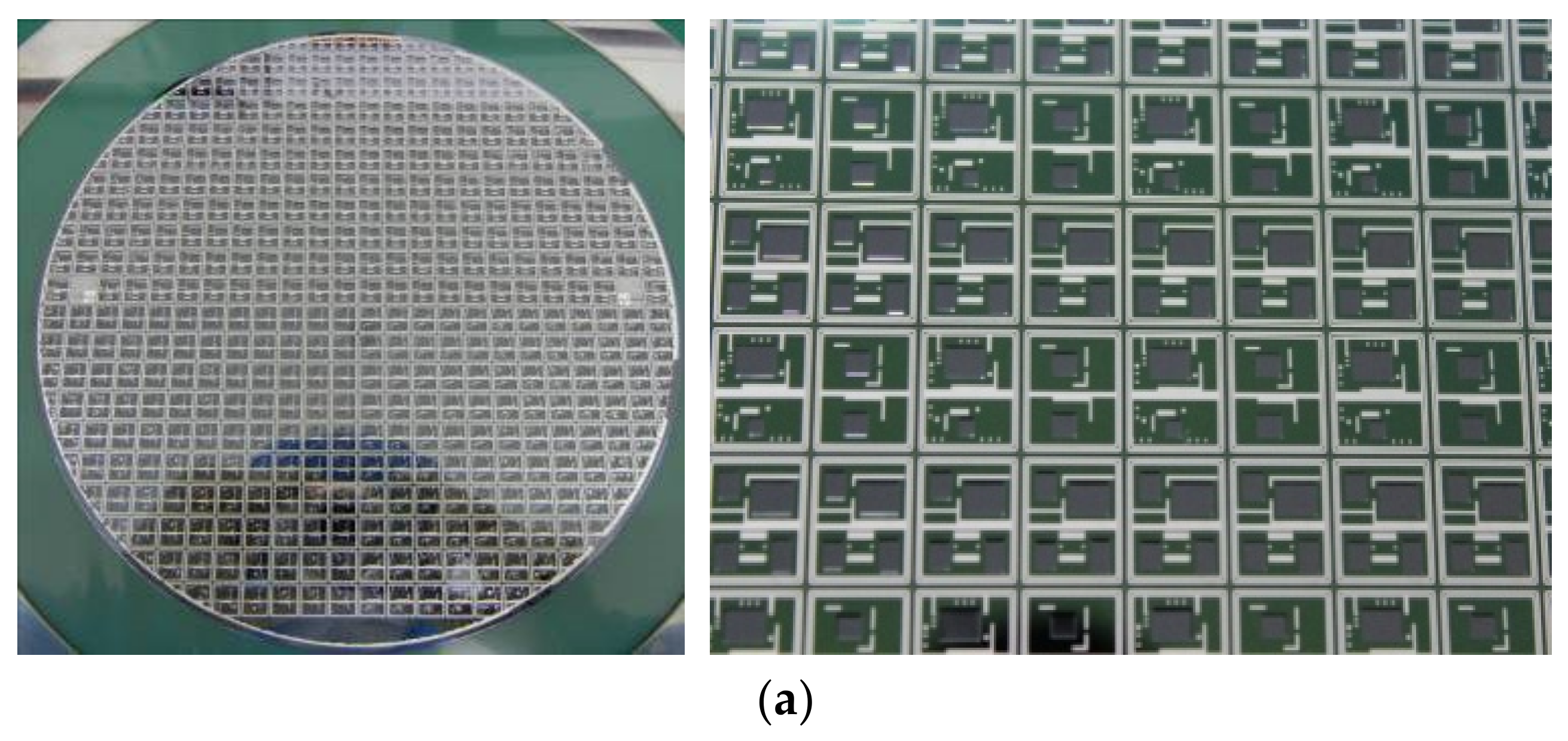
2.3. Chip Embedding with W2W Bonding

When all the processes on HR-Si interposer wafer are complete, bare dies are mounted on the front side of the 8-inch bottom interposer wafer by using conducting resin, and wire bonding is applied to connect the chip pad and the interposer with gold wire. Then, the cap interposer wafer is stacked onto the bottom interposer wafer with W2W bonding technology [17], which lasts about 30 mins inside vacuum chamber with temperatures up to 280 ℃. Finally, the interface between Cu/Ni/Pb/Au and Cu/Ni/AgSn forms one stable intermetallic compound to create hermetic enclosures for the embedded chips. The SEM images of the wafer bonding interface are shown in Figure 8.

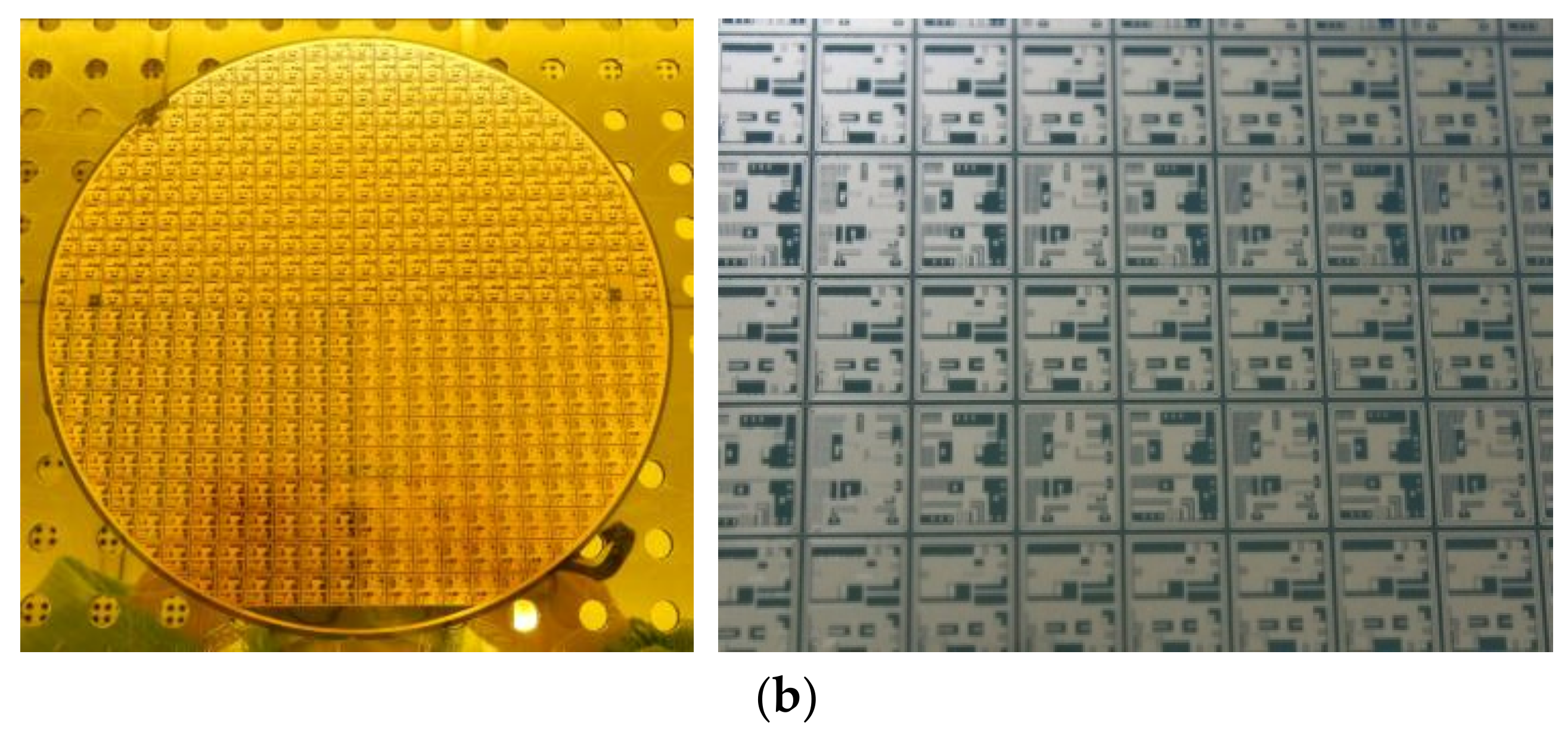
2.4. Assemblies Stacking with C2C Bonding

After W2W packaging, this 8-inch stacked wafer with embedded chips is diced to form hundreds of individual modules. Each module can be measured with the test fixture or be treated as an assembly to stack with another one to build up a four-layer stacked module. This four-layer structure broadens quite remarkably the style of 3DHI systems, increases the design flexibility, and decreases the size of multi-chips modules.
Before one of the double-stacked interposer wafers is diced into assemblies, the wafer is cleaned with standard process and electroplated Sn on one surface. Then, after wafer dicing, two assemblies are stacked again to form a four-layer stacked module by using C2C bonding technology [18], which lasts about 10 min inside vacuum chamber with temperatures up to 220 ℃ and bond force up to 30 Kg.

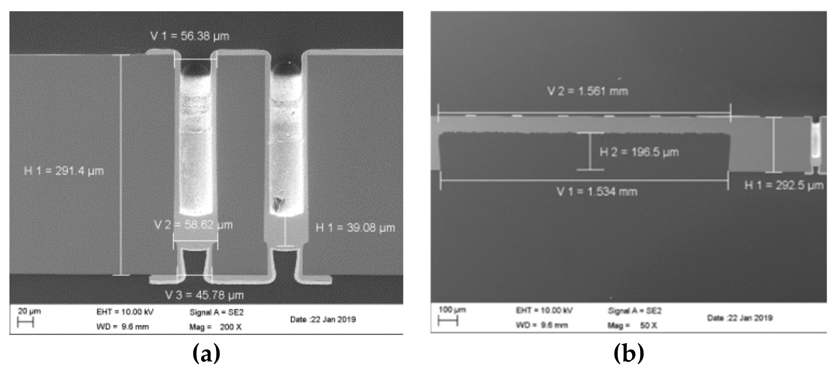
2.5. Process Verification by PCM Test

In order to assess the RF performance of the provided interposer process, the PCM structure, a 2 mm length CPW with ground on the bottom interposer, is measured on an MPIRF probe station (TS200SE) with Keysight vector network analyzer (N5230C). The PCM test setup and the device under test (DUT) are shown in Figure 9. The 2000 Ω·cm HR-Si interposer is placed on the brass chunk of the probe station, which is connected to a DC bias source. A short-open-load-through (SOLT) calibration is done by using MPIRF probes (TITAN GSG-150-µm).
According to reported experiments [19,20,21,22], if any contamination, like mobile particles or ions, adheres on the surface of HR-Si, or material defects exist within the SiO2, during the interposer process, a low-resistivity layer is created at the interface between HR-Si and SiO2. This layer increases the equivalent dielectric loss of HR-Si interposers and leads to the insertion loss increasement of the CPW. Furthermore, external DC bias between the signal line and the GND region of the CPW structure can control the formation of the low-resistivity layer and affect the degeneration of the insertion loss. Figure 10 shows the measured return loss and the insertion loss of the CPW when the bias voltage is varied in the range between 0 V to +50 V. Even though the attenuation slightly changed, a variation trend cannot be clearly found. All the measured insertion losses show about 0.18 dB/mm at 35 GHz. These experimental results indicate that great RF performance is obtained by the provided interposer process, and the HR-Si interposer has little contamination and few defects which remains similar to high resistivity RF behavior under different bias voltage.

3. The Design of Double Layers Stacked RF Module

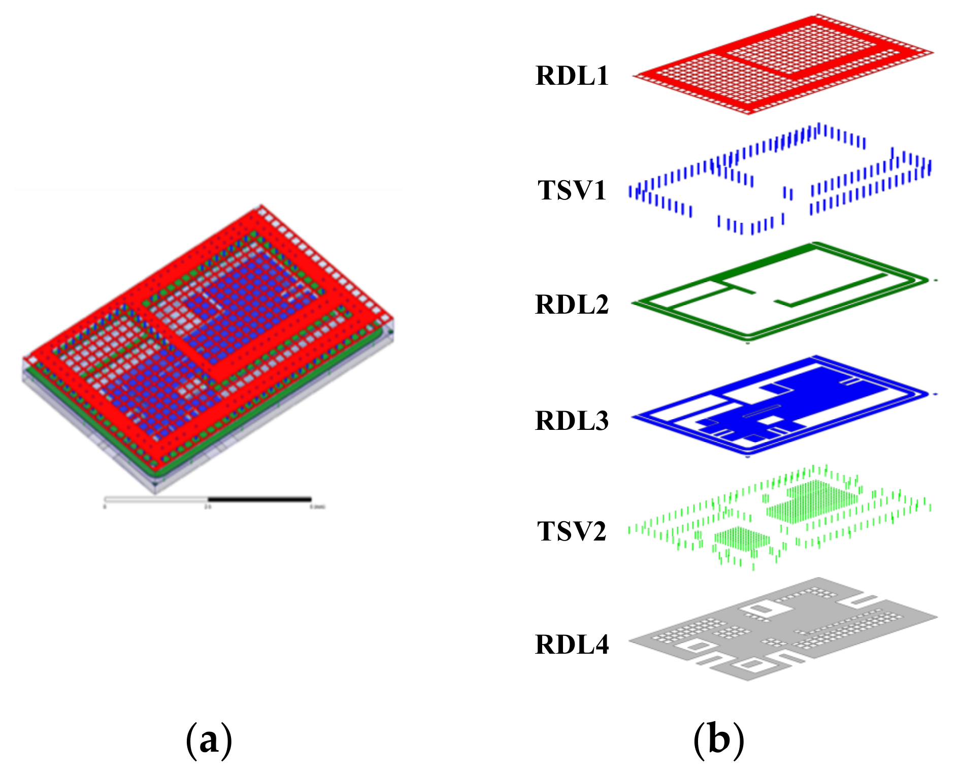
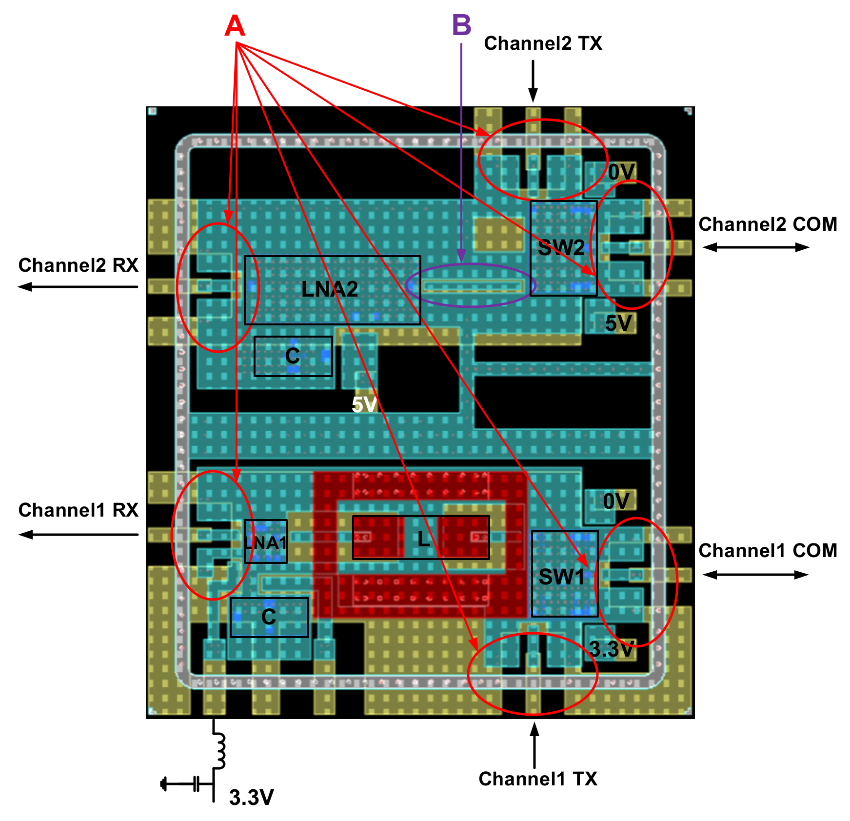
3.1. System Architecture of the RF Module

Based on the proposed 3DHI WLP process, an RF front-end module applied in UAVs is designed with two stacked interposers. The module has two receiving channels, the link budgets of which are demonstrated in Figure 11. The frequency band of the first RF channel is between 400 MHz and 600 MHz. According to the datasheet of selected low noise amplifiers (LNAs) and switches (SWs), the typical gain of the channel is about 21.2 dB and the noise figure (NF) is about 1.1 dB without considering the loss of the 3DHI package. Meanwhile, the second channel works between 2050 MHz and 2200 MHz. The gain is about 26.1 dB and the NF is about 1.4 dB.
Figure 12 shows the 3D layout rendering of the receiving channel 2 of the double stacked RF module, whose package size is 8 mm × 5 mm × 0.55 mm. The exploded view of the 3D layout of the proposed structure is shown in Figure 12b, which consists of four RDL layers and two types of TSVs. The cap interposer structure is made up of RDL1, RDL2, and TSV1 whose fabrication parameters are shown in Table 1. Meanwhile, bottom interposer structure is made up of RDL3, RDL4, and TSV2, whose fabrication parameters are shown in Table 2. The layout simulations of these are introduced below.

3.2. Simulation of the Key Structures

Figure 13 shows the top view of the module layout. The two LNAs, two SWs, and two decoupling chip capacitors are mounted on the GND pad of RDL3 layer, which are well grounded by TSV arrays. The inputs/outputs of these RF devices are connected with the bottom interposer through gold wire bonding. The 0402 lumped inductor is mounted on the RDL1 layer for the input impedance matching of LNA1. The thickness of this lumped inductance is about 0.2 ± 0.02 mm. In order to prevent increasing the depth of cavities in the cap interposer wafer, the lumped inductance is mounted on the top surface of the module.
Figure 14a shows the simplified model of the key structure for vertical RF connection (Structure A in Figure 13). As shown in Figure 14c, the 3D electromagnetic (EM) simulation provides larger than 30dB return loss and less than 0.1 dB insertion loss from 400 MHz to 2200 MHz.
For the horizontal RF connection, 50-ohm CPW lines are used to connect different RF devices like LNAs and SWs (Structure B in Figure 13). Figure 14b shows the simplified 3D EM model. The simulated results of this 1.4mm length transmission line together with gold wires provides larger than 25 dB return loss and less than 0.2 dB insertion loss from 400 MHz to 2200 MHz.

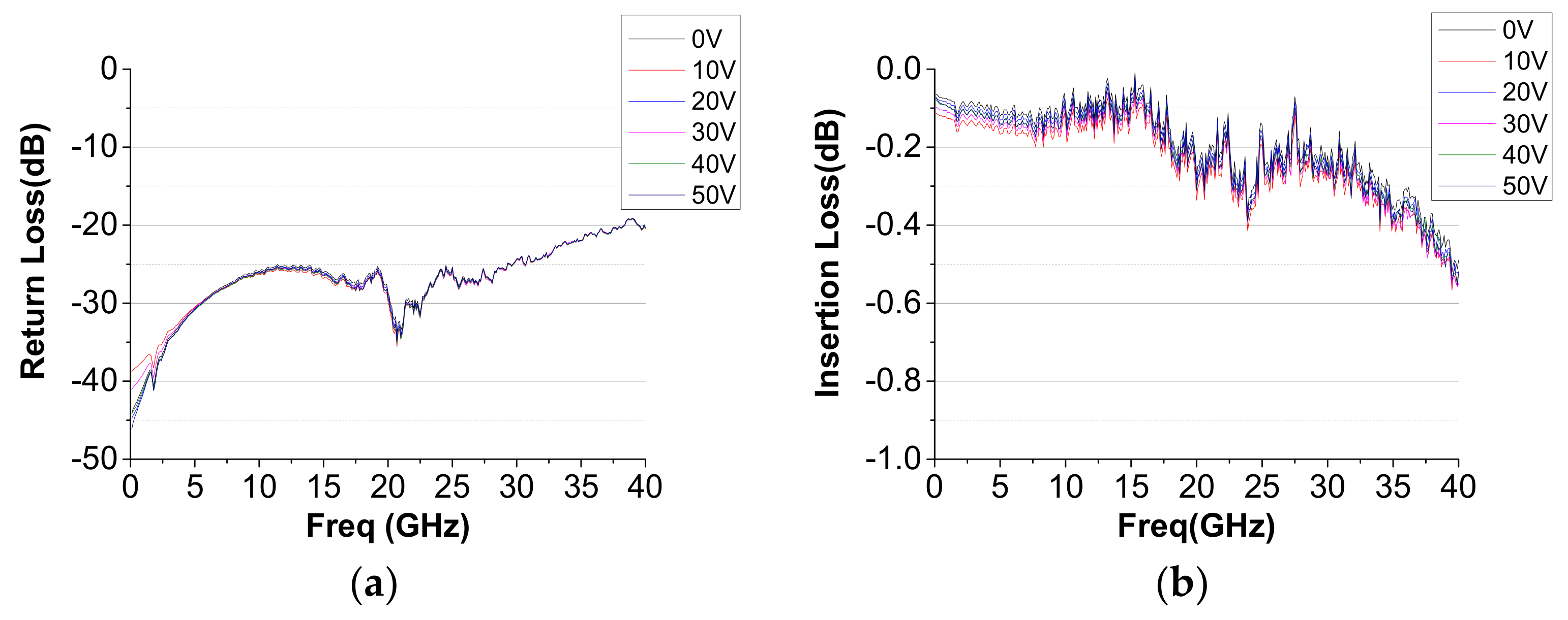
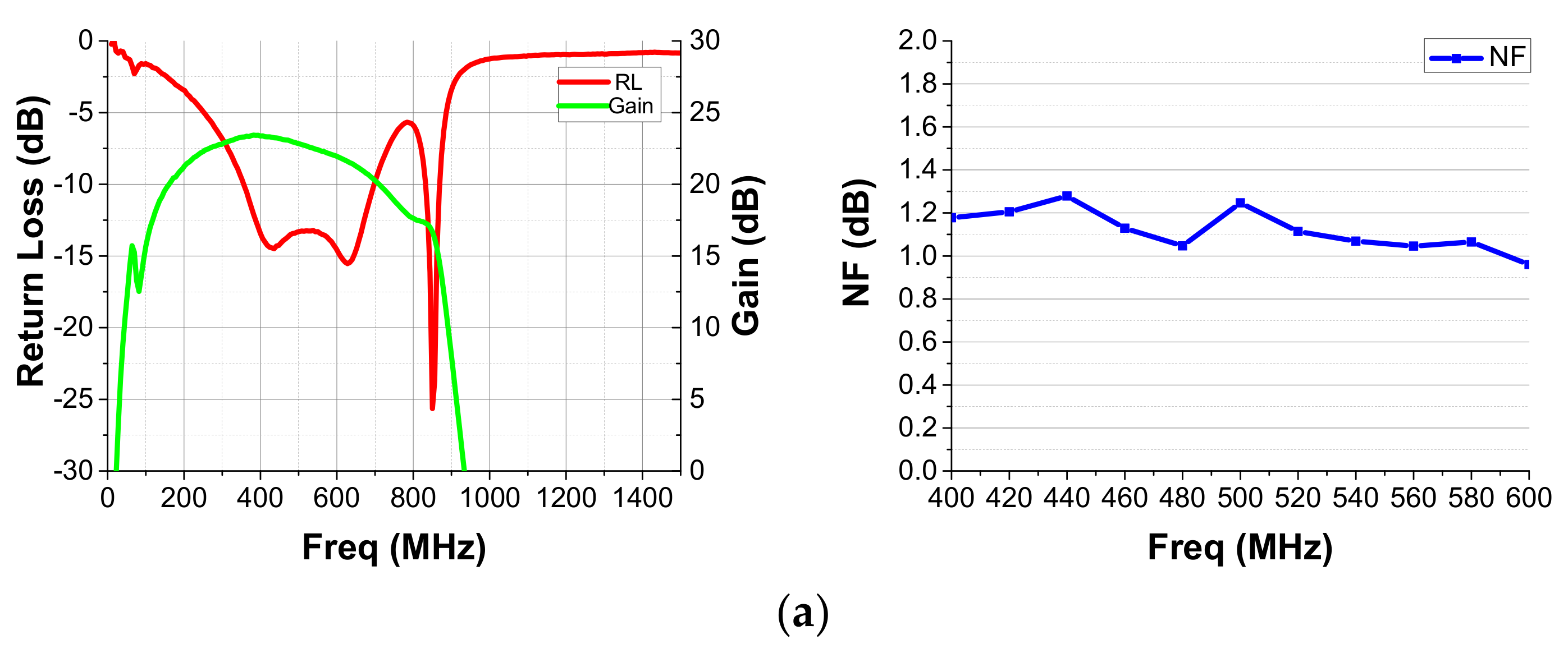
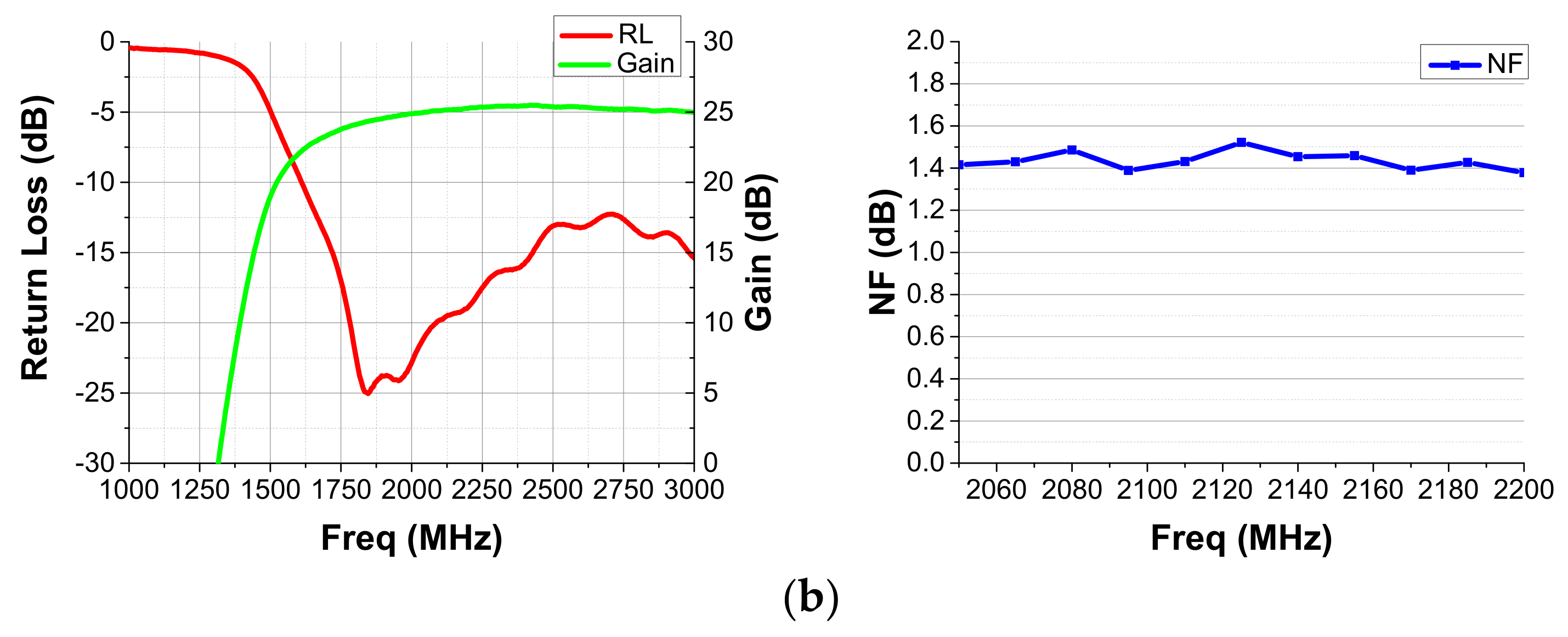
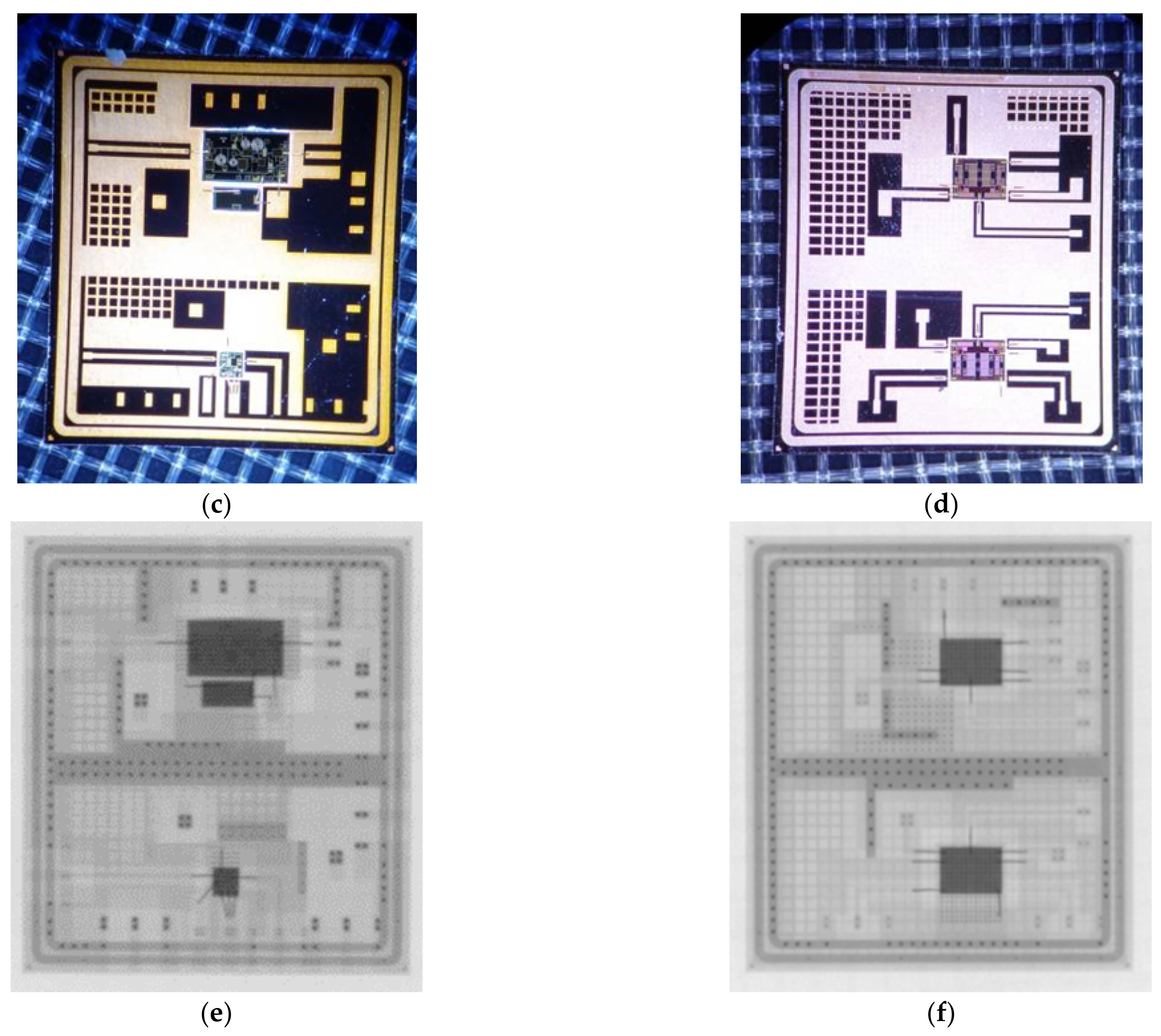
3.3. Measured Result

Following the process flow introduced in Section 2, the double stacked RF front-end module is fabricated. Figure 15 shows the 8-inch HR-Si cap and bottom interposer wafers. Figure 16 shows the diced cap and bottom interposer units with mounted RF chips and the X-ray image of the double stacked module. The double stacked package size is 8 mm × 9 mm × 0.75 mm.
The fabricated 3DHI RF front-end module is tested on an evaluation PCB board at room temperature. RF measurements are performed by using the DC power supply (N6705B) and the Keysight vector network analyzer (N5230C). As shown in Figure 17a, the NF of receiving channel 1 is less than 1.3 dB and the linear gain is larger than 22dB from 400 MHz to 600 MHz. As shown in Figure 17b, the test results of receiving channel 2 show that the NF is less than 1.5 dB and the linear gain is about 26 dB from 2050 MHz to 2200 MHz, which are similar to the link budget.
As shown in Figure 16, two turns of bonding ring are designed both on RDL2 and RDL3 layers to realize gas proof. Helium leak rate measurements, which are based on the specifications described by the MIL-STD standard [23], are applied for hermeticity tests. Excellent helium leak rates of five samples, which are at least five times smaller than the reject limit, are shown in Table 3.

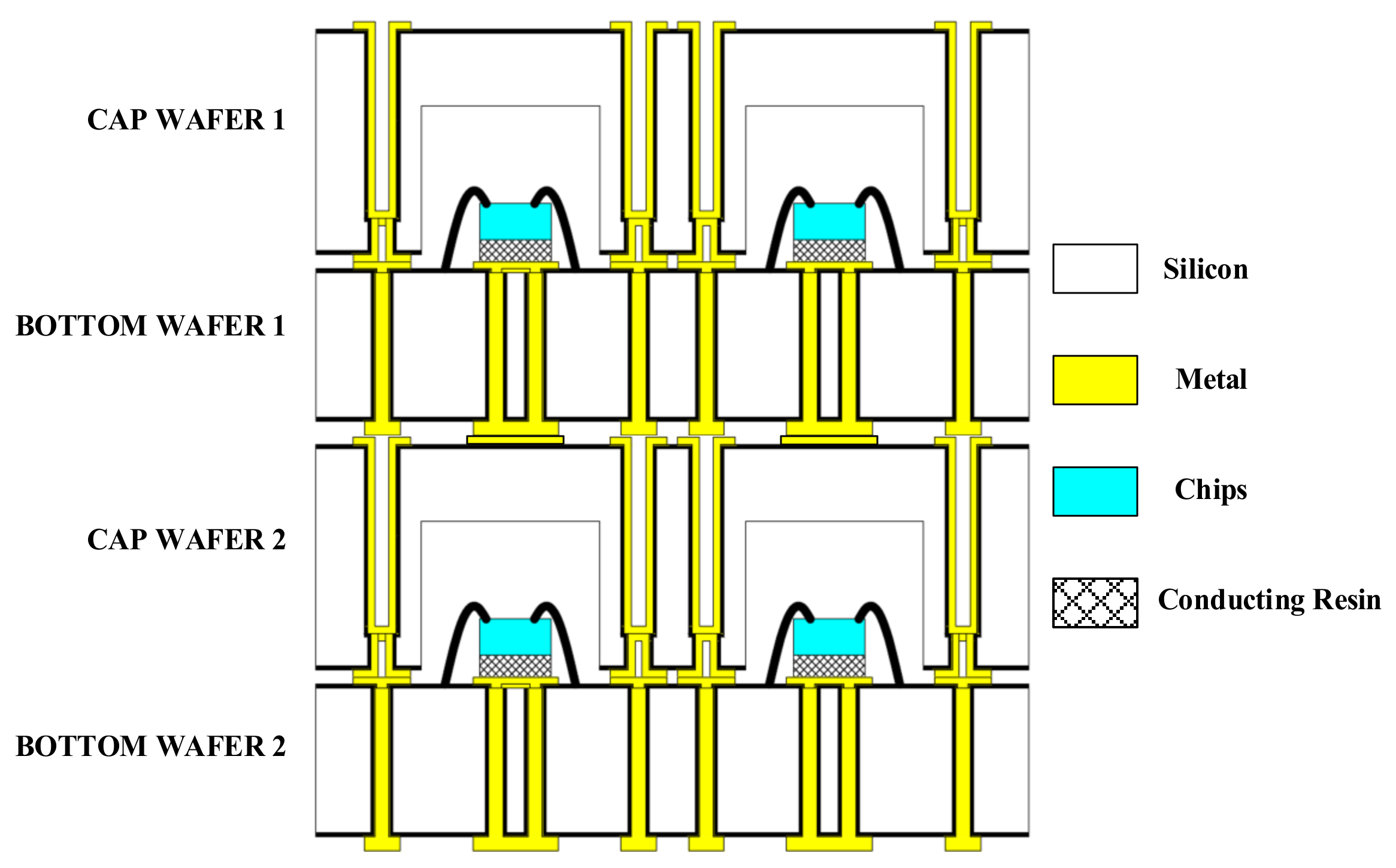
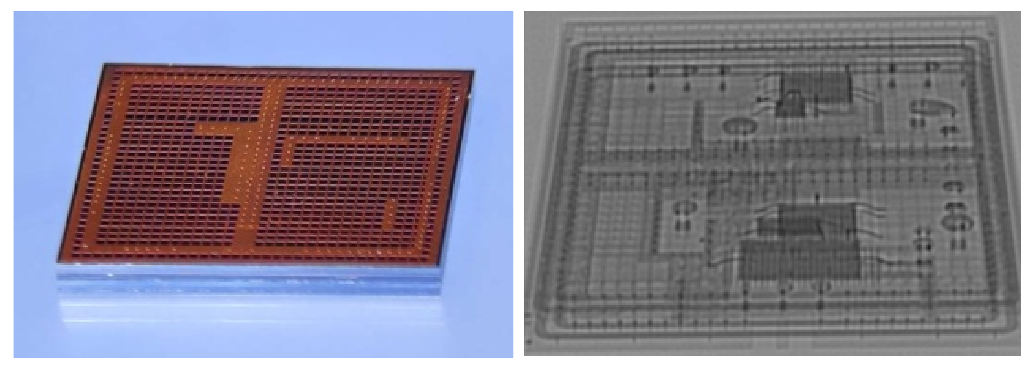
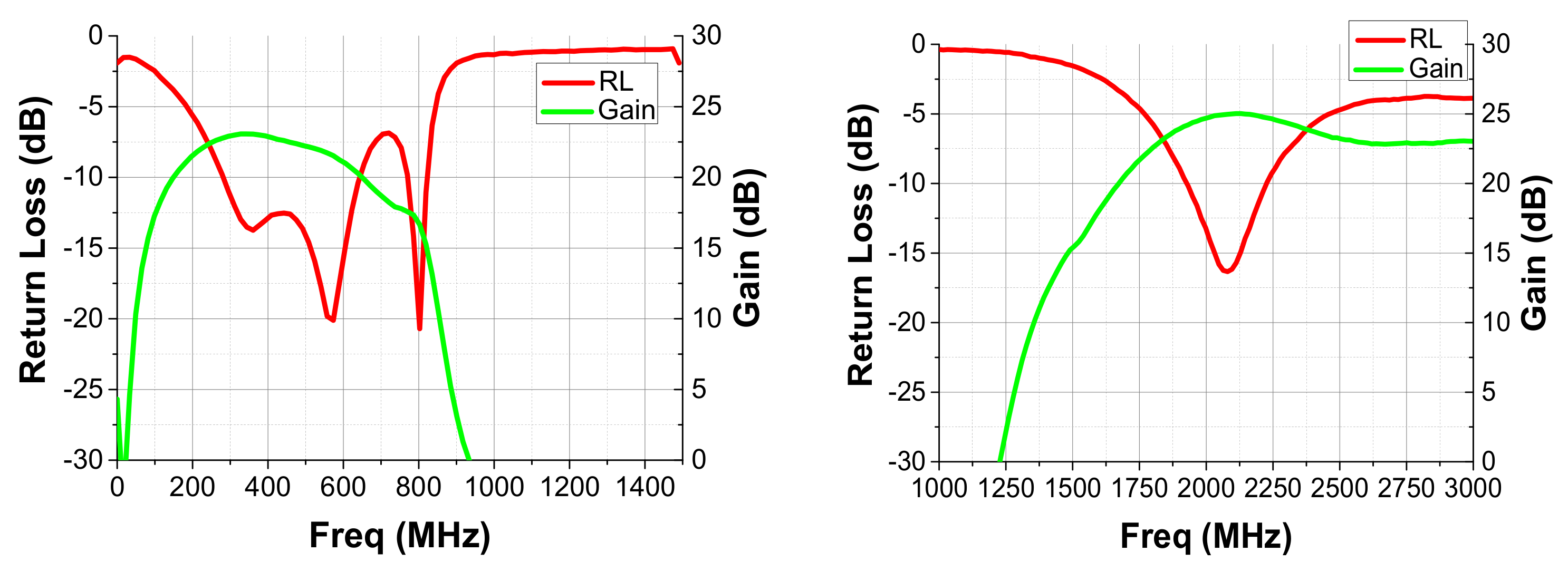
4. The Design of Four Layers Stacked RF Module

In order to validate the four-layer stacked process, the above double stacked module is re-designed as a four-layer structure, the layout of which is shown in Figure 18a,b. Same LNAs are embedded within the bottom two interposers. Meanwhile, the same RF switches are embedded within the top two interposers. The photo and the X-ray image of the fabricated four-layer stacked module are shown in Figure 18c,d and Figure 18e,f respectively.
Limited by matching the size of tooling for chip picking, the designed four-layer stacked RF module has the same size comparing to the above double stacked module, which can be further reduced due to the introduced second RF layer. Finally, the four-layer stacked package size is 8mm×9mm×1.1mm, shown in Figure 19.
The four-layer stacked RF front-end module is tested on an evaluation PCB board at room temperature. The measured results are shown in Figure 20. For receiving channel 1, the linear gain is 22.5 dB at 400 MHz and 21 dB at 600 MHz, respectively. This is smaller than tested data on double stacked module because of the relatively large insertion loss of the two additional TSVs connecting SWs and LNAs. For receiving channel 2, the linear gain is 25 dB at 2050 MHz and 24.5 dB at 2200 MHz, respectively.

5. Conclusions

In this paper, a 3DHI WLP process is proposed, and a RF front-end module with two independent UHF receiving channels are designed and implemented, which covers 400 MHz–600 MHz and 2050 MHz–2200 MHz respectively for UAV applications. The module is formed by W2W bonding of two HR-Si interposers with embedded bare dies and TSV interconnections. Double-sided DRIE and conformal electroplating process are introduced to realize the high-aspect-ratio TSV connection within 290 µm-thick cap interposer. CPW transmission lines are fabricated as the PCM, the measured insertion loss of which is less than 0.18 dB/mm at 35 GHz. The designed RF front-end module is fabricated and measured. The measured return loss and gain of each RF channel is better than 13 dB and 21 dB, and the noise figure is less than 1.5 dB. In order to evaluate the capability of the 3DHI process for multi-layer interposers, the module is re-designed and fabricated with four stacked high-resistivity silicon interposers. After W2W bonding of two pairs of interposers and wafer slicing, C2C bonding is applied to form a four-layer module with operable temperature gradient. This four-layer 3DHI process increases the design flexibility and decreases the size of multi-chips modules.

Author Contributions

Conceptualization, F.Y. and Z.W.; methodology, Q.Z.; validation, J.M., H.C.; writing—original draft preparation, Q.Z.; writing—review and editing, Z.W.; funding acquisition, J.M. All authors have read and agreed to the published version of the manuscript.

Funding

This research was funded by the National Natural Science Foundation of China, grant number of 61604128.

Data Availability Statement

The data presented in this study are available on request from the corresponding author. The data are not publicly available due to no available online server in the research group temporarily.

Acknowledgments

The authors would like to thank the Institute of Aerospace Electronics Engineering of Zhejiang University for providing the research platform and technical support.

Conflicts of Interest

The authors declare no conflict of interest.

References

  1. Sturdivant, R.L.; Ly, C.; Benson, J.F.; Hauhe, M.S. Design and performance of a high density 3D microwave module. In Proceedings of the 1997 IEEE MTT-S International Microwave Symposium Digest, Denver, CO, USA, 8–13 June 1997; Volume 2, pp. 501–504. [Google Scholar] [CrossRef]
  2. Winser, M. A single package X-Band T/R module. In Proceedings of the 2005 European Microwave Conference, Paris, France, 4–6 October 2005; p. 4. [Google Scholar] [CrossRef]
  3. Comparini, M.; Leone, C.; Montanucci, P.; Tursini, M. HTCC based Ku/IF/BB Down Converter for satellite on board processing applications. In Proceedings of the 2002 32nd European Microwave Conference, Milan, Italy, 23–26 September 2002; pp. 1–4. [Google Scholar] [CrossRef] [Green Version]
  4. Fina, A.; Di Carlofelice, A.; De Paulis, F. High Power, Thermally Efficient, X-band 3D T/R Module with Calibration Capability for Space Radar. IEEE Access 2018, 6, 60921–60929. [Google Scholar] [CrossRef]
  5. Zhou, L.; Feng, W.; Wang, D.; Shi, Y. A Compact Millimeter-Wave Frequency Conversion SOP (System on Package) Module Based on LTCC Technology. IEEE Trans. Veh. Technol. 2020, 69, 5923–5932. [Google Scholar] [CrossRef]
  6. Yu, Z.J.; Xu, Z.; Deng, Y.-K.; Zhang, Z.-G. An Overall Ltcc Package Solution for X-band Tile T/R Module. Prog. Electromagn. Res. Lett. 2013, 38, 181–192. [Google Scholar] [CrossRef] [Green Version]
  7. Khan, W.T.; Lopez, A.L.V.; Ulusoy, A.C.; Papapolymerou, J. Packaging a $W$-Band Integrated Module with an Optimized Flip-Chip Interconnect on an Organic Substrate. IEEE Trans. Microw. Theory Tech. 2013, 62, 64–72. [Google Scholar] [CrossRef]
  8. Tan, M.C.; Li, M.; Abbasi, Q.H.; Imran, M.A. Design and Characterization of T/R Module for Commercial Beamforming Applications. IEEE Access 2020, 8, 130252–130262. [Google Scholar] [CrossRef]
  9. Titz, D.; Pilard, R.; Gianesello, F.; Ferrero, F.; Luxey, C.; Brachat, P.; Jacquemod, G.; Gloria, D. Industrial HTCC Antenna-Module SiP for 60-GHz Applications. IEEE Antennas Wirel. Propag. Lett. 2012, 11, 576–579. [Google Scholar] [CrossRef]
  10. Di Carlofelice, A.; De Paulis, F.; Fina, A.; Di Marcantonio, U.; Orlandi, A.; Tognolatti, P. Compact and Reliable T/R Module Prototype for Advanced Space Active Electronically Steerable Antenna in 3-D LTCC Technology. IEEE Trans. Microw. Theory Tech. 2018, 66, 2746–2756. [Google Scholar] [CrossRef]
  11. Bang, Y.-S.; Kim, J.-M.; Kim, J.-M.; Kim, Y.-K.; Jang, Y.-H. LTCC-based vertical via interconnects for RF MEMS packaging. Microw. Opt. Technol. Lett. 2009, 52, 252–257. [Google Scholar] [CrossRef]
  12. Choi, K.-S.; Moon, S.H.; Eom, Y.-S.; Bae, H.-C.; Lee, J.H. Thermal and Electrical Designs of RF 3D Module Based on Si Interposers with Redundant TSVs. In Proceedings of the 2016 IEEE 66th Electronic Components and Technology Conference (ECTC), Las Vegas, NV, USA, 31 May–3 June 2016; pp. 2051–2057. [Google Scholar] [CrossRef]
  13. Lheurette, E.; Mounaix, P.; Salzenstein, P.; Mollot, F.; Lippens, D. High performance InP-based heterostructure barrier varactors in single and stack configuration. Electron. Lett. 1996, 32, 1417. [Google Scholar] [CrossRef]
  14. Baba, T.; Kokubin, Y.; Sakaki, T.; Iga, K. Loss reduction of an ARROW waveguide in shorter wavelength and its stack configuration. J. Lightwave Technol. 1988, 6, 1440–1445. [Google Scholar] [CrossRef]
  15. Ranganathan, N.; Lee, D.Y.; Youhe, L.; Lo, G.-Q.; Prasad, K.; Pey, K.L. Influence of Bosch Etch Process on Electrical Isolation of TSV Structures. IEEE Trans. Compon. Packag. Manuf. Technol. 2011, 1, 1497–1507. [Google Scholar] [CrossRef]
  16. Tsai, W.L.; Chang, H.H.; Chien, C.H.; Lau, J.H.; Fu, H.C.; Chiang, C.W.; Kuo, T.Y.; Chen, Y.H.; Lo, R.; Kao, M.J. How to select adhesive materials for temporary bonding and de-bonding of 200 mm and 300 mm thin-wafer handling for 3D IC integration? In Proceedings of the 2011 IEEE 61st Electronic Components and Technology Conference (ECTC), Lake Buena Vista, FL, USA, 31 May–3 June 2011; pp. 989–998. [Google Scholar] [CrossRef]
  17. Pelzer, R.; Kirchberger, H.; Kettner, P. Wafer-to-Wafer Bonding Techniques: From MEMS Packaging to IC Integration Applications. In Proceedings of the 2005 6th International Conference on Electronic Packaging Technology, Shenzhen, China, 30 August–2 September 2006; pp. 1–6. [Google Scholar] [CrossRef]
  18. Lee, J.S.; Byun, K.Y.; Chung, Q.H.; Suh, M.S.; Kim, S.C.; Kim, Y. Chip to chip bonding using micro-cu bumps with Sn capping layers. In Proceedings of the 2009 European Microelectronics and Packaging Conference, Rimini, Italy, 15–18 June 2009; pp. 1–5. [Google Scholar]
  19. Makita, T.; Tamai, I.; Seki, S. Coplanar Waveguides on High-Resistivity Silicon Substrates with Attenuation Constant Lower Than 1 dB/mm for Microwave and Millimeter-Wave Bands. IEEE Trans. Electron Devices 2011, 58, 709–715. [Google Scholar] [CrossRef]
  20. Schollhorn, C.; Zhao, W.; Morschbach, M.; Kasper, E. Attenuation mechanisms of aluminum millimeter-wave coplanar waveguides on silicon. IEEE Trans. Electron Devices 2003, 50, 740–746. [Google Scholar] [CrossRef]
  21. Wu, Y.; Gamble, S.; Armstrong, B.; Fusco, V.; Stewart, J. SiO2/interface layer effects on microwave loss of high-resistivity CPW line. IEEE Microw. Guid. Wave Lett. 1999, 9, 10–12. [Google Scholar] [CrossRef]
  22. Gamble, H.; Armstrong, B.; Mitchell, S.; Wu, Y.; Fusco, V.; Stewart, J. Low-loss CPW lines on surface stabilized high-resistivity silicon. IEEE Microw. Guid. Wave Lett. 1999, 9, 395–397. [Google Scholar] [CrossRef]
  23. Costello, S.; Desmulliez, M.P.Y.; McCracken, S.; Abraham, E.; Lowrie, C.; Cargill, S. Electrical Test Structure for the Measurement of Hermeticity in Electronic and MEMS Packages With Small Cavity Volumes. IEEE Trans. Semicond. Manuf. 2013, 26, 281–287. [Google Scholar] [CrossRef]
Figure 1. Structural diagram of the 3DHI WLP process with up to 4 stacked HR-Si interposers.
Electronics 10 01893 g001
Figure 2. Cross section of the bottom HR-Si interposer wafer.
Electronics 10 01893 g002
Figure 3. Process flow of the bottom HR-Si interposer wafer.
Electronics 10 01893 g003
Figure 4. The images of the full-via-plated TSVs. (a) X-ray image, (b) SEM image, (c) optical microscope image.
Electronics 10 01893 g004
Figure 5. Cross section of the cap HR-Si interposer wafer.
Electronics 10 01893 g005
Figure 6. Process flow of the cap HR-Si interposer wafer.
Electronics 10 01893 g006
Figure 7. The SEM images of the cap wafer. (a) conformal-plated TSVs, (b) cavities.
Electronics 10 01893 g007
Figure 8. SEM images of the wafer bonding interface. (a) 1000× with TSVs, (b) 4000× without TSVs.
Electronics 10 01893 g008
Figure 9. Photos of the PCM test setup and the DUT. (a) Probe station, (b) the CPW.
Electronics 10 01893 g009
Figure 10. The measured result of PCM structure. (a) Return loss, (b) insertion loss.
Electronics 10 01893 g010
Figure 11. System architecture and link budget of the two channel RF front-end module.
Electronics 10 01893 g011
Figure 12. 3D layout rendering of the receiving channel 2 of the double stacked RF module.
Electronics 10 01893 g012
Figure 13. Top view of the layout of the double stacked RF front-end module.
Electronics 10 01893 g013
Figure 14. Key RF structures of the module with 3D EM simulation results. (a)simplified model of A structure, (b) simplified model of B structure, (c) simulation of A structure, (d) simulation of B structure.
Electronics 10 01893 g014
Figure 15. Photos of the 8-inch HR-Si cap and bottom interposer wafers.
Electronics 10 01893 g015aElectronics 10 01893 g015b
Figure 16. Photos of the diced bottom and cap interposer units and the X-ray of the double stacked module.
Electronics 10 01893 g016
Figure 17. Measured results of the double stacked 3DHI RF front-end module. (a) Test result of channel 1, (b) test result of channel 2.
Electronics 10 01893 g017aElectronics 10 01893 g017b
Figure 18. 4-layer stacked RF front-end module: (a) Layout of the bottom two layers, (b) layout of the top two layers, (c) photo of the bottom unit, (d) photo of the top unit, (e) X-ray of the bottom unit, (f) X-ray of the top unit.
Electronics 10 01893 g018aElectronics 10 01893 g018b
Figure 19. The photo and the X-ray image of the 4-layer stacked RF front-end module.
Electronics 10 01893 g019
Figure 20. Measured results of the 4-layer stacked 3DHI RF front-end module.
Electronics 10 01893 g020
Table 1. Process parameters of the bottom interposer wafer.
Num in Figure 2Layer/ViaMaterialThickness (µm)
1φ30 µm TSVCu190
2SiO2 (PECVD)SiO21.6
3RDL1Cu5
Ni/Pd/Au3/0.1/0.05
4PIPI4
5RDL2Cu5
Ni/Au3/0.05
Table 2. Process parameters of the cap interposer wafer.
Num in Figure 6LayerMaterialThickness (µm)
1φ60 µm TSVCu250
2SiO2 (Thermal oxidation)SiO20.1
3RDL1Cu5
Ni/Au3/0.05
4φ50 µm TSVCu40
5SiO2 (PECVD)SiO21
6RDL2Cu5
Ni1
SnAg5
7Cavity 200
Table 3. Fine helium leak rate measurements.
Sample NumberMeasured Result
(Pa.cm3)/s
Reject Limit
(Pa.cm3)/s
#019.2 × 10−45 × 10−3
#027.7 × 10⁻⁴
#037.5 × 10⁻⁴
#046.2 × 10⁻⁴
#052.2 × 10⁻⁴
Publisher’s Note: MDPI stays neutral with regard to jurisdictional claims in published maps and institutional affiliations.

