Abstract
IoT technology is evolving at a quick pace and is becoming an important part of everyday life. Consequently, IoT systems hold large amounts of data related to the user of the system that is vulnerable to security breaches. Thus, data collected by IoT systems need to be secured efficiently without affecting the IoT systems’ performance and without compromising security as well. In this paper, a high-performance dynamic security system is introduced. The system makes use of the ZedBoard’s dynamic partial reconfiguration capability to shift between three distinct cipher algorithms: AEGIS, ASCON, and DEOXYS-II. The switching between the three algorithms is performed using two different techniques: the algorithm hopping technique or the power adaptive technique. The choice of which technique to be used is dependent on whether the system needs to be focused on performance or power saving. The ciphers used are the CAESAR competition finalists that achieved the greatest results in each of the three competition categories, where each cipher algorithm has its own set of significant characteristics. The proposed design seeks to reduce the FPGA reconfiguration time by the application of LZ4 (Lempel-Ziv4) compression and decompression techniques on the ciphers’ bitstream files. The reconfiguration time decreased by a minimum of 38% in comparison to the state-of-the-art design, while the resource utilization increased by approximately 2%.
1. Introduction
The Internet of things (IoT) is a network connecting devices that have unique identifiers to the internet [1,2]. These devices have sensors or actuators that enable them to gather data from their surroundings and take actions depending on the collected data, which can change their state [2]. IoT technology applications are increasing and spreading every day. The technology is used in a variety of applications to make daily life smarter and easier by connecting all of the devices and can be operated from anywhere and at any time easily [2]. One of the applications that illustrate the power of IoT technology is smart homes where all of the devices in the building are connected to the internet and linked with each other. Consequently, mobile phones can be used to manage the devices easily [2]. The number of IoT devices is rapidly increasing and it is predicted to exceed 18 billion by 2022 [3]. However, as the number of IoT-connected devices increases, so does the amount of the gathered data by IoT systems. Since the information acquired by IoT devices may be linked to businesses, governments, or people, protecting this information is crucial.
IoT systems are resource-constrained systems, meaning they have hardware and power consumption restrictions. Additionally, IoT systems are continuously connected to the internet for data transmission. Thus, IoT systems are vulnerable to security breaches that can compromise the data of the users. Accordingly, lightweight cryptography has evolved to address the IoT systems’ security problem, as it can ensure the safety of the information related to the users from security breaches [4]. Lightweight cryptography can be defined as encryption algorithms that need a small area for its implementation, consumes less power, has a shorter processing time, and is less expensive [5]. Lightweight cryptography’s main application is in resource-limited systems such as IoT systems since they have constraints on their power usage and hardware utilization.
Due to the limitations on hardware, area, and the power of IoT systems, the reconfigurability of FPGAs (Field Programmable Gate Arrays) provides the flexibility that allows the implementation of IoT applications and the limitations of the system being easily overcome [6]. One of the most important characteristics of FPGAs is dynamic partial reconfiguration (DPR), which allows for reprogramming of portions of the FPGA during operation to alter functionalities. The DPR can lead to a decrease in area utilization of the design, a decrease in power consumption, and an increase in system flexibility for updates [6,7].
In Soliman et al. [3], the authors introduced a security system design that used the algorithm hopping technique, which is derived from the frequency hopping technique. The design interchanges between five lightweight cryptographic algorithms in a random manner using the algorithm hopping technique where the swap is performed using dynamic partial reconfiguration. The design obtained good results in terms of area; nevertheless, the time necessary to reconfigure the FPGA was lengthy since it was reliant on the size of the security algorithms’ bit files. In Samir et al. [7], the authors introduced an energy adaptive security system. The design interchanges between five lightweight cryptographic algorithms based on the system’s current power level and employs the dynamic partial reconfiguration feature for the algorithm’s switching. The design produced adequate power results; nevertheless, the FPGA reconfiguration time was lengthy due to the cipher algorithms’ bit file sizes. In Sellers et al. [8], the authors presented a partially reconfigurable design that utilizes compression techniques. The authors employed compression techniques to decrease the size of the bitstream files of the static partition of the design. The design produced acceptable results that supported the impact of compression in the size of the static module; however, the reconfiguration time of the dynamic modules was not taken into account.
Consequently, an efficient IoT security system is presented in this work. The system utilizes three lightweight cryptographic algorithms: ASCON, AEGIS, and DEOXYS-II, all of which were CAESAR competition finalists. The DPR is utilized to interchange between the three cipher algorithms during FPGA operation. Two approaches are used to choose between the algorithms: the first approach involves randomly choosing the cipher algorithm to achieve better security. The second approach depends on the power level of the system in the algorithm choice. However, since time is needed to interchange between the three algorithms using DPR depending on their respective bit files sizes, the LZ4 compression/decompression algorithm was utilized. LZ4 is a fast, lossless compression algorithm that is a derivative from the LZ77 compression algorithm [9]. LZ4′s compression speed is similar to that of the previous algorithms, but it has a faster decompression speed. Its decompression speed can reach up to a few GB/s per core [9]. The usage of hash-based matching search and match overlapping is one of the best benefits that contribute to the LZ4 algorithm’s faster decompression rates [9]. Thus, LZ4 was selected to be used in the proposed design to improve the reconfiguration time. Figure 1 illustrates the block diagram of the proposed design flow.
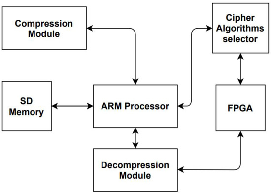
Figure 1.
Design Flow block diagram.
This paper’s sections are structured as follows: Section 2 provides an overview of the design and background on the design methodologies. Section 3 describes the entire hardware design of the proposed system, including how each module is constructed on both the hardware and software levels. Section 4 summarizes the results and findings. Then, in Section 5 the paper is concluded.
2. Background and Design Overview
2.1. Encryption/Decryption Algorithms
The three cryptographic cipher algorithms utilized in the proposed architecture are presented in this section. The three ciphers were the finalists in the CAESAR competition (Competition for Authenticated Encryption: Security, Applicability, and Robustness) [10]. Each of the three algorithms has its advantages and disadvantages, for example, ASCON is a lightweight algorithm (requires low memory), AEGIS has the highest performance of the three, and DEOXYS-II (containing the misuse resistance) has the highest defense in depth. The CAESAR competition’s three categories are [10]:
- Algorithms to be utilized in lightweight applications (resource-constrained environments).
- Algorithms to be utilized in applications requiring high performance.
- Algorithms that have depth in defense.
The winner of each category was ASCON, AEGIS, and DEOXYS, respectively. The three algorithms are reviewed in the following sections.
2.1.1. AEGIS
AEGIS is a well-known authenticated encryption method for network packets protection. AEGIS is high-performance encryption that is also a suitably authenticated cipher for network communications [11]. Its fundamental building block is AES round functions, which are utilized for encryption. [12]. AEGIS is a fast and efficient method with excellent security since the key and state can never be retrieved if the initialization vector is not utilized again [11]. Some of the main features of the AEGIS algorithm are [12]:
AEGIS efficiency is better than AES-GCM as it was tested on Intel Haswell microprocessors and its speed was twice that of the AES-GCM algorithm. Its computational cost is also half that of AES-GCM. The encryption and decryption modules of AEGIS use the same algorithm, and the authentication provided by the AEGIS algorithm is stronger than that provided by the AES-GCM algorithm, making it a stronger security algorithm.
2.1.2. ASCON
ASCON is a lightweight algorithm that has a good performance in both hardware and software platforms as it has an efficient side-channel resistance features implementation [13]. ASCON mainly utilizes a reduced number of instructions and it targets parallelizing the instructions as much as possible [13]. Consequently, ASCON is considered to be suitable for applications that require good performance and smaller areas [13]. Some of the main features of ASCON are as follows [13]:
ASCON has flexible and lightweight hardware where it utilizes 10 kGE to achieve throughput around 4.9–7.3 Gbps. ASCON is a bit sliced in software where permutation implementation is defined in terms of a word of size 64 bits. This implementation facilitates its usage in processors with small word sizes and it can use the processors’ pipelining and parallelization features.
2.1.3. DEOXYS
DEOXYS-II is an authenticated encryption algorithm that is primarily based on tweakable block ciphers. As a primary building block, DEOXYS-II employs the AES round function [14]. When used for small messages, it has the best performance [15]. DEOXYS-II operates in two modes: the first mode is nonce respecting and the second mode is nonce misuse resistant [3]. In the proposed design, the nonce misuse resistant mode is employed to be able to reuse the same N with the same key without facing any danger of ciphertext extraction. Some of the main features of DEOXYS are as follows [15]:
DEOXYS has very good performance for software implementation since it utilizes the parallelized modes that decrease the cycle per byte counts. The speed of the nonce respecting mode of DEOXYS is faster than AES-GCM. Additionally, DEOXYS has high efficiency for small messages. This is because DEOXYS is a tweakable-based cipher that avoids precomputations. Accordingly, DEOXYS is considered very efficient for lightweight applications and internet applications, where for lightweight applications the size of the messages sent are usually small (few bytes), similarly, internet applications packet have considerably small sizes.
2.2. Algorithm Hopping
Frequency hopping is a spread spectrum communication technique that works by the alteration of the frequency of transmission periodically. The technique functions by interchanging between several frequency channels using a pseudorandom sequence known to both transmitter and receiver [16]. The fast switching between frequencies in the transmission will decrease the undesired interception or jamming of the transmitted signals [16]. The pseudorandom pattern leads to unpredictability of the transmission frequencies, which ensures the security of the transmission [16].
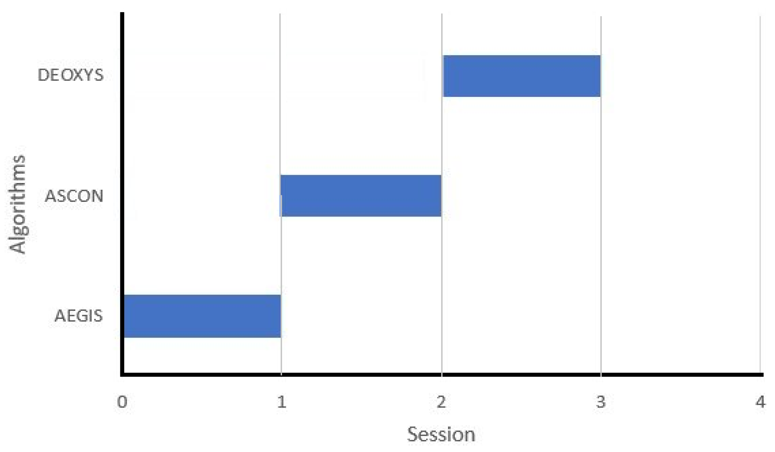
The algorithm hopping technique is derived from the frequency hopping technique. In the algorithm hopping technique, frequency channels are equivalent to security algorithms and the data to be encrypted by the security algorithms is equivalent to the radio signal sent over the frequency channels. The pseudorandom patterns that are needed to interchange between the different algorithms are generated using LFSR (linear feedback shift register). Consequently, the data will be encrypted using a different algorithm in each period where the selection of the algorithm is random according to the LFSR output. Figure 2 illustrates the application of the algorithm hopping technique in the proposed design to interchange between the ciphers per session.

Figure 2.
Algorithm Hopping Technique.
2.3. Dynamic Partial Reconfiguration
2.3.1. DPR Definition
Partial dynamic reconfiguration is a feature available in FPGAs that enables the changing of the design implemented on the FPGA during its runtime [17]. Full bit files are utilized for the first configuration of the FPGA and partial bit files are utilized to update the reconfigurable parts of the FPGA. The process only changes the reconfigurable FPGA parts without altering or affecting the other regions running on the FPGA that won’t be reconfigured [18,19].
FPGAs, when using the dynamic partial reconfiguration feature, are divided into two partitions: the static part and the dynamic part. The static part is the FPGA partition that will not be altered or reconfigured during FPGA run time. The dynamic partition is the part that will have its configuration changed or updated during FPGA runtime [17]. As illustrated in Figure 3, the light grey part represents the static part of the design while the dark grey part (labeled as Reconfig Block “A”) represents the dynamic part. The reconfiguration of the FPGA functions by changing the partial bit file in Reconfig Block “A” by one of the bit files (A1.bit, A2.bit, A3.bit, A4.bit) where the selection of the bit files depends on the need of the design [17].
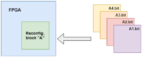
Figure 3.
Dynamic Partial Reconfiguration illustration [3].
The DPR feature enables the dynamic time multiplexing of portions of the FPGA logic, which can offer many advantages, for example, the area needed on the FPGA for the implementation of several functions can be decreased, which, consequently, can lead to power consumption decrease and cost reduction [17]. Additionally, it enables more flexibility in the algorithms and protocols that can be utilized for the same application. Ain addition, it utilizes new techniques in the security of design; fault tolerance can be enhanced and configurable computing can be much faster [17].
2.3.2. Xilinx AXI-HWICAP Controller
Xilinx presents several IP cores that can be used for the interfacing of Xilinx’s ICAP primitive with the user system design. Xilinx ICAP controller’s main functionality is enabling the embedded microprocessors such as micro blaze and ARM processors to have access to the configuration memory [20]. ICAP is a Xilinx FPGA hard macro that allows direct access to the configuration memory in read and write modes. The ICAP interface data width ratio to the configuration memory ratio is 8 bits, 16 bits, or 32 bits wide in the Xilinx 7 series [20].
The maximum theoretical throughput for reconfiguration using ICAP is 400 MB/S if the data width has a size of 32 bits and the frequency of the clock is 100 MHz [20]. The throughput of reconfiguration using the ICAP measured in a real-time application is less than the theoretical throughput due to the reconfiguration overhead added to the dynamic partial reconfiguration at the system level design [20]. There are two different ICAP controllers designed for different buses such as the AXI-HWICAP controller, which is used for AXI buses interfaces where the controller is connected to the bus as a slave peripheral [20].
Xilinx Hardware Internal Configuration Access Port (HWICAP) is an IP core for the AXI-bus interface that enables an embedded microprocessor as the ARM processor to read and write in the FPGA configuration memory by exploiting the internal configuration access port (ICAP) [21]. HWICAP is used for writing the software programs that update the structure of the circuit and also its functionality during the operation of the FPGA [21].
AXI-HWICAP’s main features can be summarized as follows: AXI-HWICAP supports resource reading, it can support reading long frames [21]. AXI-HWICAP enables read/write of the configuration logic block and the lookup tables [21]. It also enables the read/write of the configuration logic block flip flop properties. Additionally, AXI-HWICAP has an ICAP arbitration interface that eases the distribution of the ICAP with other blocks and enables safe hand-off [21].
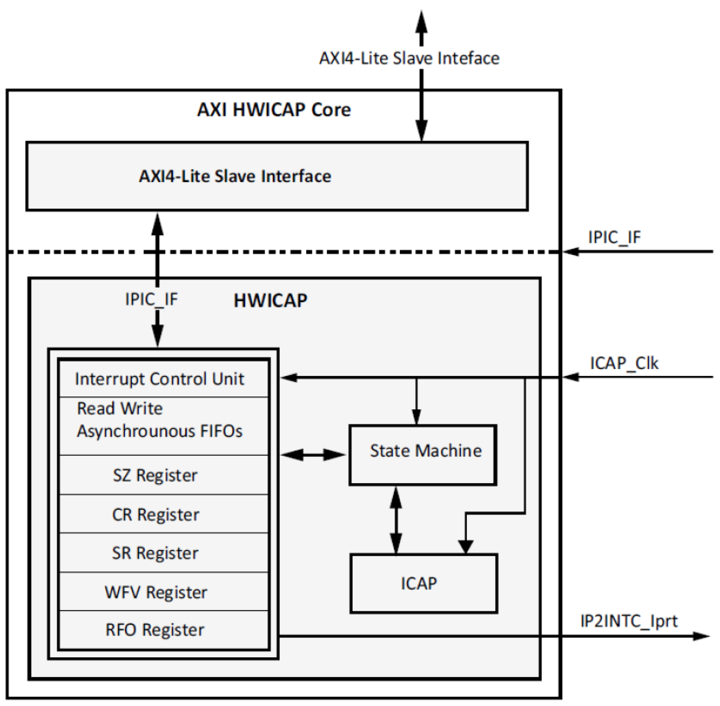
The AXI-HWICAP controller has the needed interface that allows the data transfer to and from the ICAPEn [20]. To write to the ICAPEn, the data required to be written is first stored in a Write FIFO, then the data is passed to the ICAPEn [21]. The AXI-HWICAP also offers read back of the data from ICAPEn where the data is read into the read FIFO. Figure 4 demonstrates the AXI-HWICAP block diagram [21].
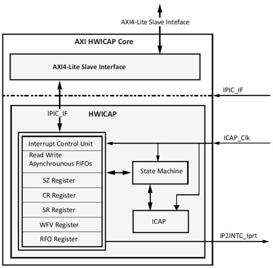
Figure 4.
AXI-HWICAP block diagram [3].
2.3.3. Configuration of FPGA using DPR
FPGA configuration is started by loading the full design image file upon the FPGA start-up. After the FPGA is configured fully and operational, partial bit files can be exploited at any time to configure the regions predefined as reconfigurable, whereas the remaining part of the FPGA stays fully active, uninterrupted, and doesn’t have its configuration changed [22].
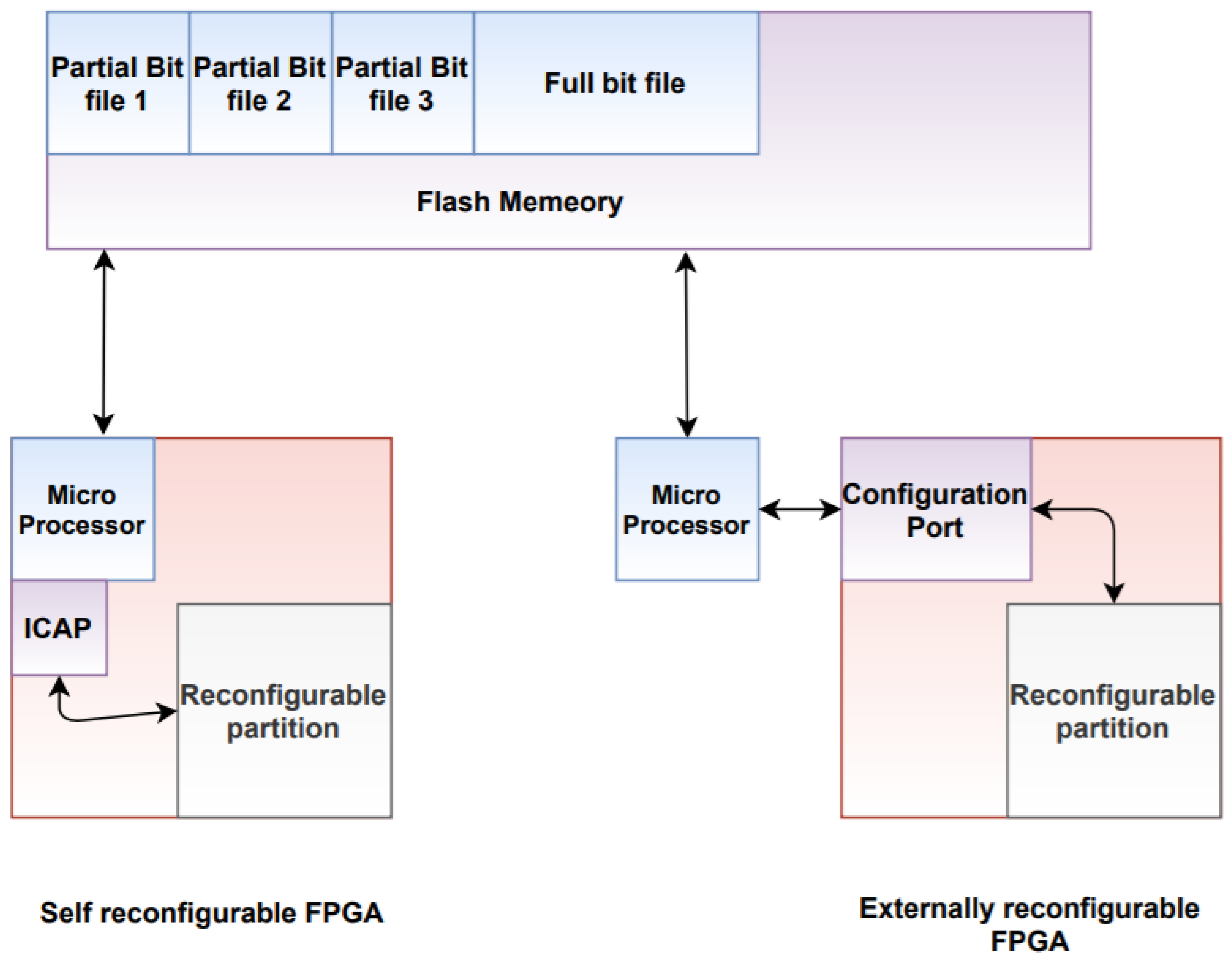
Some of the configuration ports that can be utilized for loading the partial bitstream for the partial reconfiguration are Slave SelectMAP, Slave Serial, JTAG, or Internal Configuration Access Port (ICAP). Typically, partial bitstreams are stored in the flash memory and bitstream transfer can be achieved by a microprocessor or by routines programmed into the FPGA [22]. Different techniques can be utilized for the initialization of the reconfiguration and the delivery of the partial reconfiguration image, as demonstrated in Figure 5.
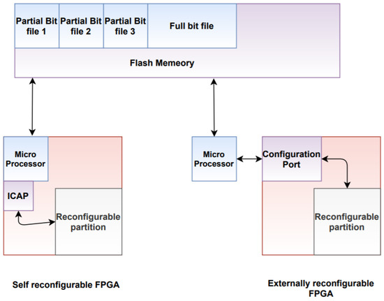
Figure 5.
Partial bit file delivery.
As illustrated in Figure 5, in a self-reconfigurable FPGA, a small microprocessor is used to fetch the partial bit file from the flash memory, and then the fetched data is sent to the ICAP [22]. Usually, a state machine is utilized to fetch the partial bit files and send the bit files to the ICAP, meaning that the microprocessor won’t be needed in this case [22].
However, in an externally reconfigurable FPGA, a much simpler solution is applied where an external processor is utilized to fetch the partial bit file from the flash memory, and then the file to the FPGA configuration port [22].
Partial bitstreams contain all the needed commands and the necessary data for the partial reconfiguration. Full FPGA configuration and dynamic partial reconfiguration are both managed by the same FPGA engine; accordingly, the same type of programming information is handled by the same programming mechanism [22]. Loading a partial bitstream in the FPGA does not need the location of the reconfigurable module. This is because the configuration frame addressing the information is added in the partial bitstream, so it will not be sent to the wrong part of the FPGA [22].
2.4. LZ4 Compression Algorithm
LZ4 is a very fast, lossless compression algorithm based on the LZ77 compression algorithm. It can reach a compression speed of more than 500 MB/s per core which is scalable with a multicore CPU. Furthermore, it has a very fast decoder and its speed can reach multiple GB/s per core, which is the speed limit of the RAM on multicore systems [23]. LZ4 is an asymmetric compression algorithm in the same way as the LZSS algorithm meaning that the decompression of these algorithms is much simpler and faster than its compression. The decompression process is the same as that of the LZ77 algorithm where it depends on copying literal from the decoded part [23].
Originally, LZ4 was a form of compressed data format. LZ4 sequences found in compressed data files consist of a token, literal length, offset, and match length [24].
The token’s main functionality is to determine the length of matched and unmatched characters [24]. The literal length is defined as the length of the data that is still not compressed and its value is equivalent to the value of the length of uncompressed data minus 15. The literal main functionality is the storage of the uncompressed data in the LZ4 sequence where it is copied from the original data [25]. When data that has occurred before is found during scanning of the data input, this data will be compressed. The offset value denotes the current data address minus the prior data address [25]. Match length is known as the length of the matching data. LZ4 algorithm procedure comprises five main steps which are hash computation, matching, backward matching, parameter calculation, and data output [25].
2.5. Proposed Design Overview
The proposed design is presented in this section where it uses a compression module in DPR-based designs to reduce the reconfiguration time. To shift between the three algorithms most effectively for power consumption and area utilization reduction, a partial dynamic configuration feature of FPGAs is utilized. The DPR feature is used to interchange between the three winning cipher algorithms of the CAESAR competition ASCON, AEGIS, and DEOXYS. The switching between the three ciphers is performed using two methods: the algorithm hopping technique or the power adaptive technique.
The choice of the compression algorithm to be utilized in the proposed design depends on which algorithm could achieve the highest decrease in the reconfiguration time. Three LZ compression algorithms were used to determine the algorithm that can reach the best reconfiguration time: LZSS, LZW, and LZ4. LZ4 achieved the highest reduction in the reconfiguration time of the FPGA, so it was selected to be utilized in the proposed design implementation.
In the algorithm hopping technique, the interchanging between the three lightweight cryptographic algorithms is performed in a pseudorandom pattern. The pseudorandom pattern is output from the LFSR module. The selection procedure is as follows: first, a seed is inserted into the LFSR, after that the LFSR generates a pseudorandom sequence with a new ID to designate which algorithm will be used first, and after the first session is finished, the LFSR generates a new pseudorandom sequence with a new ID. The cycle is repeated each time the FPGA is reconfigured to choose the algorithm that will be used.
The power adaptive technique switches among the three algorithms according to the IoT end-device system power level. This means that the algorithm with the highest power consumption is used when the system power level is the highest. When the system power level is intermediate the algorithm is switched to the algorithm with the next lower power consumption. At the lowest power level of the system, the algorithm with the lowest power consumption is used.
Due to the usage of dynamic partial reconfiguration, the proposed design is divided into two parts: the static part and the dynamic part. The static part contains the communication protocols, inputs and outputs ports, and several APIs that link different design partitions together. The dynamic part contains the center of the design, which contains a reconfigurable partition. The reconfigurable part holds the cipher algorithm chosen by either the LFSR pseudorandom pattern or depending on the system power level. The algorithms are interchanged using the DPR. The flow of the design as shown in Figure 1 is illustrated as follows: first, when the FPGA is launched, the compression module begins extracting the bit files of the cipher algorithms from the memory to compress them. The compressed files are saved in the memory to be utilized in the FPGA reconfiguration.
The cipher algorithm selector block is the block that decides the algorithm to be utilized. This block could be either a linear feedback shift register (LFSR) or a selector that selects the algorithm according to the current power level of the system.
After that, the selected algorithm bit file is extracted from the memory and sent to the programmable logic. Then, the programmable logic reconfigures the FPGA partially by using the bit file output from the decompression module. The cycle is repeated except for the compression operation, which is only executed once at the first initialization of the FPGA to produce the compressed bit files of the cipher algorithms.
3. Methodology and Proposed Design
3.1. Design Modules
The use of the dynamic partial reconfiguration feature in the design led to partitioning the design into a static part and a dynamic part. The static part remains unchanged during the FPGA runtime, while on other hand the dynamic part is the part that uses the DPR feature to update the configuration during FPGA runtime.
The static part contains the modules:
- LFSR (Linear Feedback Register)
- FIFOs (First in first out)
- AEAD top module
- Compression module
- Decompression module
The dynamic part contains the modules:
- Preprocessor
- Cipher core
- Postprocessor.
The design modules are demonstrated in more detail in the following subsections.
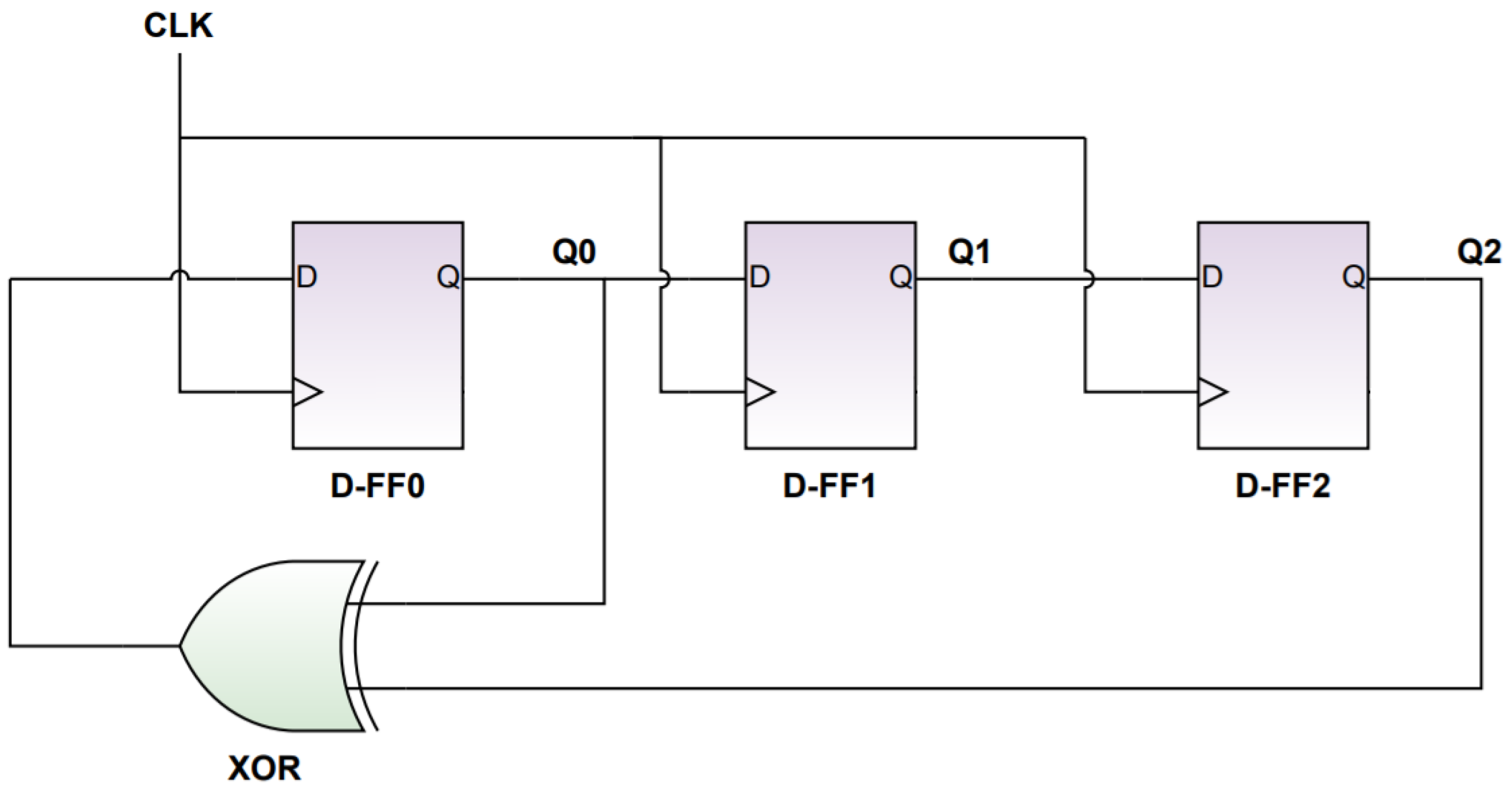
3.1.1. Linear Feedback Shift Register (LFSR) Module
The linear feedback shift register is a shift register that creates a sequence of binary values [25]. The sequences produced from the LFSR, which are repetitive periodically, are known as pseudorandom sequences [25]. After the LFSR, feedback paths are used and they are known as taps. The taps consist of either exclusive OR or exclusive NOR. They are used mainly for the production of random series in the feedback path [25]. The D flip flops are exploited as the LFSR registers. Figure 6 demonstrates the structure of the 3-bit LFSR configuration.
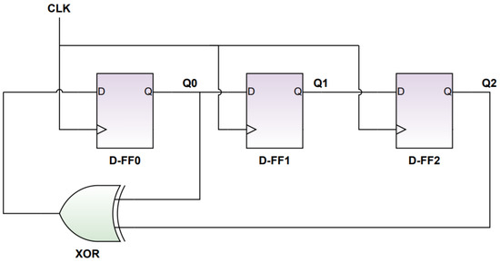
Figure 6.
Three-bit LFSR Design.
The flip flops’ role in the configuration is acting as shift registers so they can generate pseudorandom sequences. The taps values can produce the polynomial equation, which in turn creates the repeating sequences [26]. The produced sequence can be deterministic because after definite repetitions the sequence restarts at the original value. This is why the sequence is known as pseudo [26].
In the proposed design, the LFSR is needed to choose between three different cipher algorithms so only two bits are needed for this choice. However, to provide a more random pattern to protect the choice, a three-bit LFSR is utilized in the proposed design. To start the pseudorandom sequence generation, a seed is inserted as an initial input value to the LFSR.
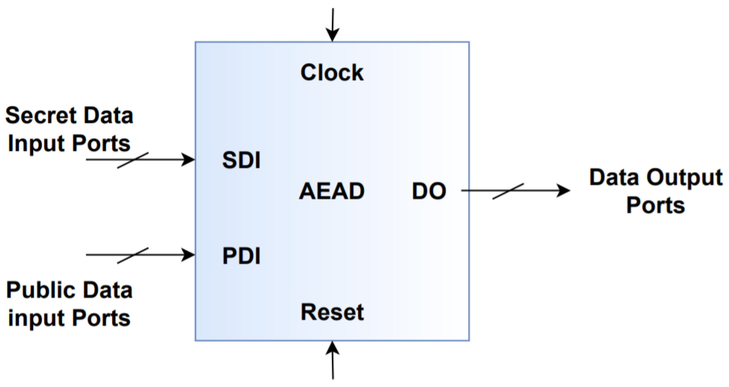
3.1.2. AEAD Top Module
AEAD top is a hardware API where its main functionality is interfacing with the CAESAR competition ciphers. AEAD comprises specifications needed for interfacing with the cipher core, the communication protocols, and its formats utilized in both inputs and outputs from and to the ciphers [27]. Additionally, it includes the timings dependencies necessary for all the data and control signals passing into the ciphers [27].
The AEAD presents many features to make its usage easier. These features include having inputs of different sizes in bytes, data port width can vary from 8 bits to 256 bits, the capability of communicating with simple passive devices such as FIFOs, and support of different communication protocols easily [27]. Additionally, it can support encryption and decryption in the same core [27].
The AEAD Top interface comprises three main data buses [27]:
- Public Data Inputs (PDI)
- Secret Data Inputs (SDI)
- Data Outputs (DO)
AEAD top consists of several control signals that are utilized in handshaking such as valid and ready. The valid signal is used to specify whether there is data ready to be sent at the source. The ready signal is utilized to determine whether the destination is ready to receive data to its side [27].
Public data inputs (for instance the message, associated data, and public message number) are split up from the secret data inputs (for instance the key) to have improved resistance against any possible attacks that may use the public data manipulated by the attacker to be used as a new key [27].
Some of the other parameters that can be used in the AEAD API are key length, data block size, SDI port width, PDI port width, and type of data padding, which are altered depending on each cipher’s specifications [27]. In the proposed design, to decide on the length of each of the parameters, the largest of the parameters of each cipher is chosen and then they are grouped in one static port so that they can be exploited by each of the dynamic ciphers. Figure 7 demonstrates the block diagram of the AEAD module.
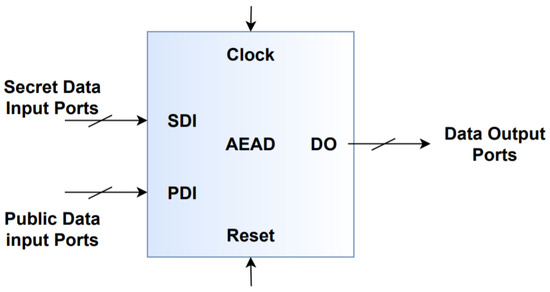
Figure 7.
AEAD Interface block diagram.
3.1.3. First In First Out (FIFO) Module
The clock domain can be described as a segment of logic where all of its synchronous elements, such as flip flops, synchronous RAM blocks, etc., are functioning at the same clock frequency [28]. There are two different clock domains in the proposed design, one for the programmable logic and one for the processing system.
The flow of data between two different clock domains is as follows: first, data arrives at one of the clock domains at random time intervals with different frequencies. Some of the time intervals may contain a larger load of data traffic [28]. The receiving device is located on another clock domain; accordingly, it can process the data at a rate different from that of the transmitting device [28]. Therefore, a queue of data is formed in the FIFOs. The FIFOs are asynchronous, consequently, data can arrive at the transmitter side at random time intervals. On the receiver side, the data is fetched from the queue if it has the bandwidth for its processing [28].
In the proposed design, FIFOs modules are utilized with the AEAD module. FIFOs are placed at the data ports of the AEAD module to act as a boundary between the processing system and the programming logic. Figure 8 illustrates the block diagram of the AEAD module after the addition of FIFO modules.
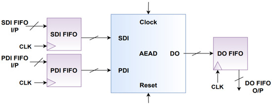
Figure 8.
AEAD Module with FIFOs at its inputs and outputs.
3.1.4. Preprocessor Module
The preprocessor module is one of the components of the AEAD API that is utilized for interfacing with the CAESAR competition ciphers. Consequently, it has similar tasks performed for all the ciphers. Its main functionality is making the input data compatible with the cipher core. Some of the tasks executed by the preprocessor module are [27]:
- Activating the keys and loading them.
- Using Serial in Parallel Out mode to load the data to the input blocks.
- The padding of the input blocks.
- Monitoring the number of data bytes that are left and still need processing.
3.1.5. Postprocessor Module
The Postprocessor module is another component of the AEAD API exploited for interfacing with the CAESAR competition ciphers and it has the same tasks performed for all the ciphers. Some of the tasks carried out by the module are [27]:
- Clearing the output blocks from any data not relevant to ciphertext or plaintext.
- Using Parallel-In, Serial-Out mode to output the blocks into words.
- Converting the output words into segments.
- Storing decrypted messages in FIFOs, till the authentication verification is finished.
- Producing the status block that contains the authentication output.
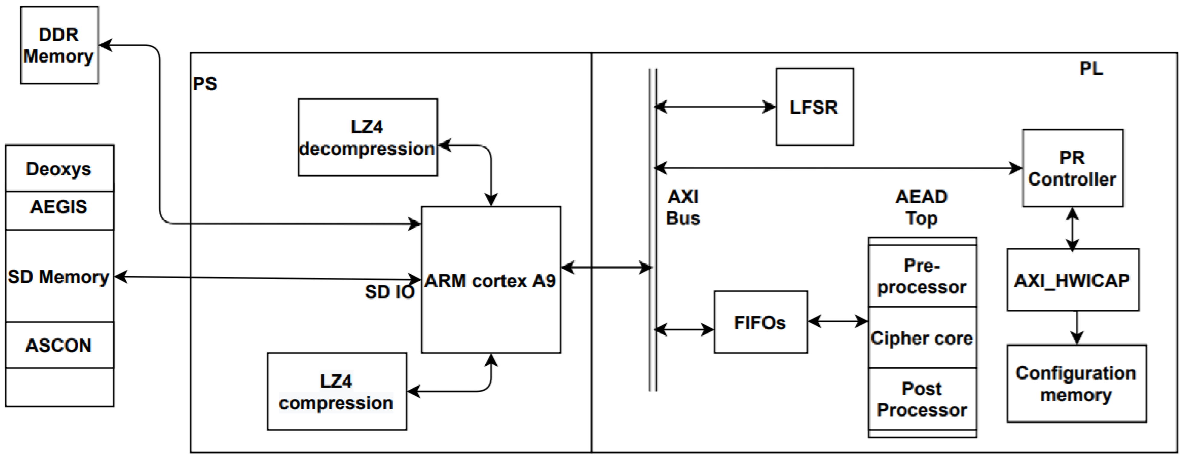
3.2. Hardware Design
The proposed design aim is to improve FPGA reconfiguration time in DPR-based designs used in IoT security applications. In the proposed design, the partial dynamic reconfiguration feature of the FPGAs is utilized to switch between the three different cryptographic cipher algorithms. The selection of the algorithm to be used in the reconfiguration of the FPGA is performed by either the algorithm hopping technique or the power adaptive technique. Additionally, uploaded bitstream compression and decompression are performed using the LZ4 compression algorithm to decrease the FPGA reconfiguration time.
The design is implemented on an FPGA integrated with ARM (Advanced RISC machine) cortex processor on the same chip. The DPR feature of FPGAs is used, which is a feature that enables the modification of FPGAs at runtime. The design comprises two main partitions: static partition and dynamic partition. First, the dynamic part contains the reconfigurable modules, where each of the reconfigurable modules has its corresponding partial bit file. Consequently, when one of the ciphers is needed to reconfigure the FPGA, its corresponding bit file is transferred to the FPGA side. Thus, the static part of the FPGA remains unchanged during FPGA reconfiguration since only the dynamic part is modified.
AXI-HWICAP (Hardware Configuration Access Port) DPR controller is utilized since its resource utilization is less than other controllers. ICAP is a predefined Xilinx macro that has straight access to the configuration memory for both write and read modes.
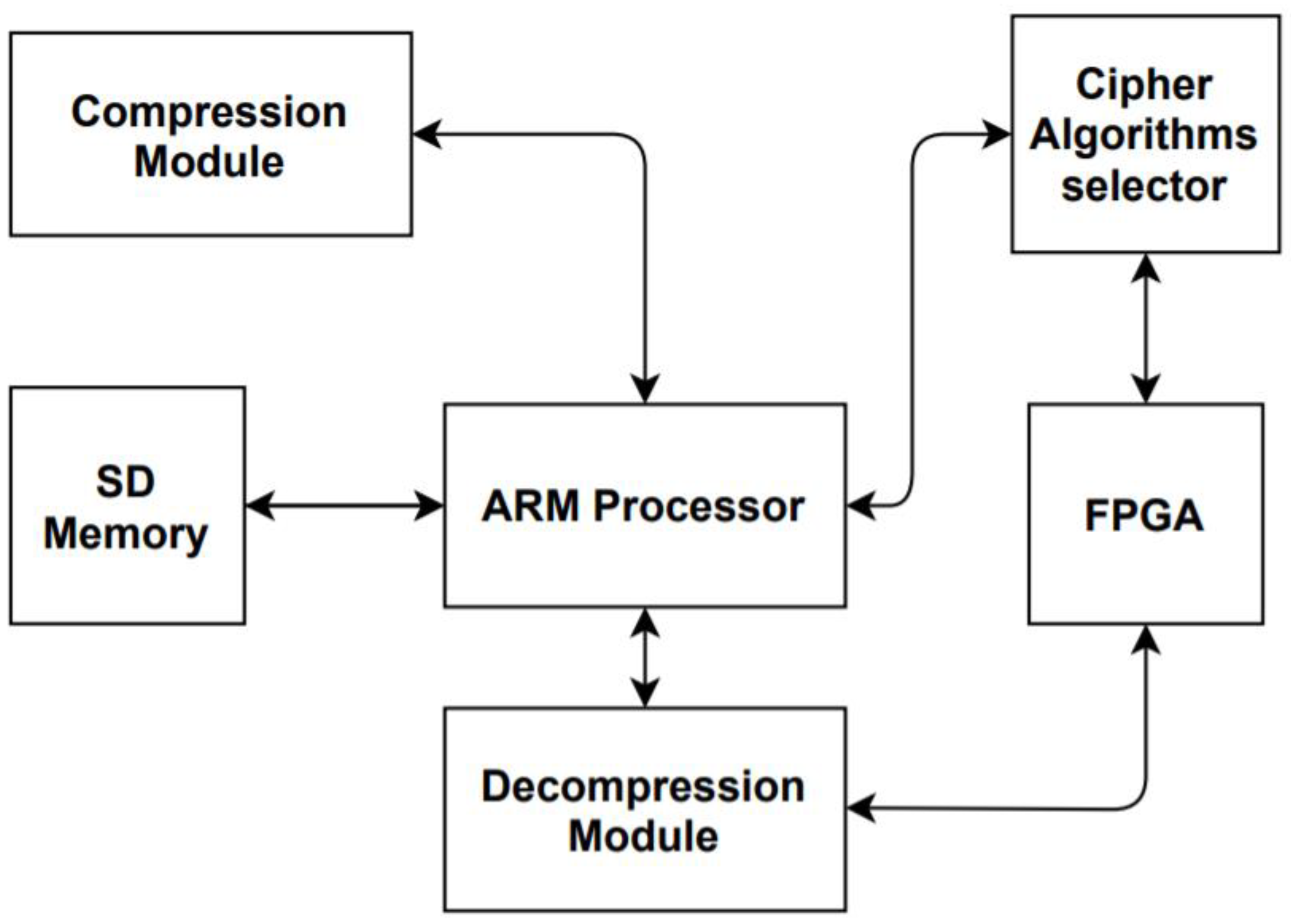
The hardware design as demonstrated in Figure 9 illustrates the components of the two partitions of the architecture where the static part contains the following modules: First In First Out (FIFOs) module, AEAD top, LFSR, compression module, and decompression module. The dynamic part contains the preprocessor module, cipher core, and postprocessor module. In the design proposed, the use of the compression algorithms to compress the bitstream’s files will reduce the time required for fetching the bit file from the memory. Therefore, the reconfiguration time will be decreased. On the other hand, the area and power consumption of the design are slightly affected. For the implementation of the previously mentioned compression/decompression of the bitstreams on the FPGA, an algorithm with a high compression ratio and high decompression rate is required. Hence, the LZ4 algorithm was the most suitable compression algorithm for this application.
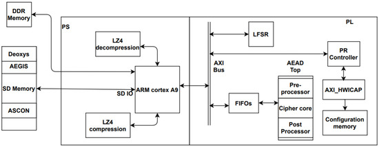
Figure 9.
Proposed design hardware diagram.
As shown in Figure 9, the LZ4 compression module is implemented in the processing system (PS) side to decrease the cipher bit file size. The LZ4 decompression module is implemented on the PS side as well. It has small runtime in the processor as the decompression rate of the LZ4 algorithm can exceed 1000 Mb/s. Accordingly, the processing time of the decompression module is very small and will not negatively affect the reconfiguration time.
According to the algorithm selector technique used, the design can have two variations whose flows will be explained as in the below subsections.
3.2.1. Algorithm Hopping-Based Design
The design flow of the encryption process in the algorithm hopping-based design works as follows:
First, upon the first start of the FPGA, the ciphers bitstreams are fetched from the memory then passed to the compression module to be compressed by using the LZ4 algorithm. Second, the initial seed and the LFSR enabler are inserted into the LFSR module to begin the generation of the pseudorandom sequence. Third, the LFSR module outputs two random bits that are utilized as the ID to determine the cipher algorithm to be used to reconfigure the FPGA. Fourth, the selected cipher bitstream is transferred to the processing system side. Fifth, the ARM cortex processor sends the compressed bitstream file to the decompression module to decompress the file. Lastly, the AEAD top configuration is changed using the selected cipher algorithm by using the DPR feature. Next, the test vectors are loaded into the FIFOs to begin encryption of the data. The above sequence is the same for all cycles excluding the compression of the bitstreams and inserting the seed to the LFSR since both operations are only done upon FPGA first start.
3.2.2. Power Adaptive-Based Design
The design flow of the encryption process in the power adaptive-based design is similar to the algorithm hopping-based design except for the cipher algorithm selection. The design flow is as follow:
First, when the FPGA is first powered up, the bitstream files of the cipher algorithms are fetched from the memory and passed to the LZ4 compression module. Then, the compressed bitstream files are saved in the memory. To reconfigure the cipher core with the desired algorithm DPR is used. The selection of the cipher algorithm is dependent on the IoT end-device system power level. When the system power level is high, the highest performance algorithm (AEGIS) is chosen. When the power level is intermediate, the algorithm with the intermediate power consumption (DEOXYS) is deployed. Finally, when the system power level runs low, the algorithm with the least power consumption (ASCON) is deployed.
According to the system power level, the respective compressed algorithm bitstream file is fetched from the memory, passed to the decompression module to decompress the bitstream file to its original form. The bitstream file is then used to reconfigure the cipher core. After the reconfiguration of the cipher core, the encryption process starts. Similar to the algorithm hopping-based design, the compression process is only performed once at the start of the FPGA.
4. Results
Xilinx Zynq-7000 SoCXC7Z020 (ZedBoard) was exploited for the design implementation and the programmable logic (including the LZ4 compression algorithm) was synthesized using Xilinx Vivado 2016.4. For the decompression algorithm implementation in the ARM processor, the SDK (software development kit) was utilized. The results recorded in the design are reviewed in this section where it is divided into three parts: the first part reviews the results of the presented design. The second part discusses the results of the algorithm hopping-based design in comparison with the state-of-the-art design. The third part discusses the results of the power adaptive system in comparison with the state-of-the-art system.
4.1. Results of Compression Algorithms
To determine the most suitable compression algorithm to be utilized in the proposed design, the bitstream files of the cipher algorithms are compressed using the three compression algorithms LZSS, LZW, and LZ4. The results of the three compression algorithms are illustrated in Table 1.

Table 1.
Compression algorithms compression ratios.
The results show that the LZ4 compression algorithm achieved the best overall compression ratios, meaning that it will contribute to decreasing the reconfiguration time better than the other compression algorithms used.
4.2. Results of the Presented Design
First, the results of the synthesization of each cipher algorithm are as illustrated in Table 2, which shows the resource utilization of each algorithm design.
Table 2.
Resource utilization of the design.
These results demonstrated that the AEGIS algorithm has the highest resource utilization. The ASCON algorithm recorded a small resource utilization, while the DEOXYS algorithm recorded the least resource utilization.
The LZ4 compression algorithm recorded decent compression ratios as demonstrated in Table 3. This shows the impact of using the LZ4 compression algorithm on the three bitstream files utilized in the design.
Table 3.
Comparison between Bit files sizes before and after compression.
As illustrated in Table 3, all the bit files of the three ciphers algorithms had the same size before compression. This is because the algorithms are using the same RP (reconfigurable partition) that has a fixed area on the FPGA. Consequently, after the decompression process is completed, all the bit files will have their original sizes before being used in the reconfiguration. The reconfiguration time in the proposed design is computed by using the throughput of the ICAP and the size of the input bit file where:
Reconfiguration Time = Size of input file(bits)/Throughput of ICAP.
In the proposed design, the decompression time is added to the reconfiguration time so:
Reconfiguration Time = Input file Size(bits)/Throughput ICAP + Decompression. Time.
The throughput of the ICAP is calculated at 10 MHz frequency and is equal to 415. Thus, we can infer that the reconfiguration time is enhanced as illustrated in Table 4. Table 4 shows the reconfiguration time after the compression and decompression modules are added.
Table 4.
Total Reconfiguration time after Compression.
4.3. Results of Algorithm Hopping-Based Design
First, the results of the reconfiguration time of the presented design in comparison with the reconfiguration time in the state-of-the-art design [3] are as illustrated in Figure 10. The comparison is between the reconfiguration time of the three algorithms used in the state-of-the-art design and the presented design.
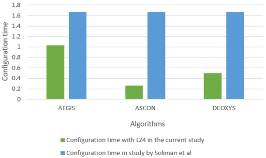
Figure 10.
Comparison between configuration time of the proposed design and the previous study.
The bitstream files of the three ciphers algorithms have the same reconfiguration time since the bit files are utilizing the same reconfigurable partition, which has a fixed area on the FPGA. On the other hand, in the proposed design, the reconfiguration time is not equal for all the bit files since each bit file has a different decompression time. Therefore, we can deduce that the proposed design enhances the reconfiguration time and reduces it with significant ratios in comparison with the state-of-the-art design.
Second, the maximum resource utilization results are reviewed. The maximum resource utilization achieved in the presented design is achieved when the AEGIS algorithm is used for reconfiguring the FPGA. In the state-of-the-art system, the maximum resource utilization was reached when deploying the COLM algorithm. The comparison is illustrated in Figure 11. The maximum resource utilization of AEGIS is lower than COLM by about 21%.
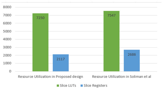
Figure 11.
Maximum resource utilization in the proposed design and the state-of-the-art system.
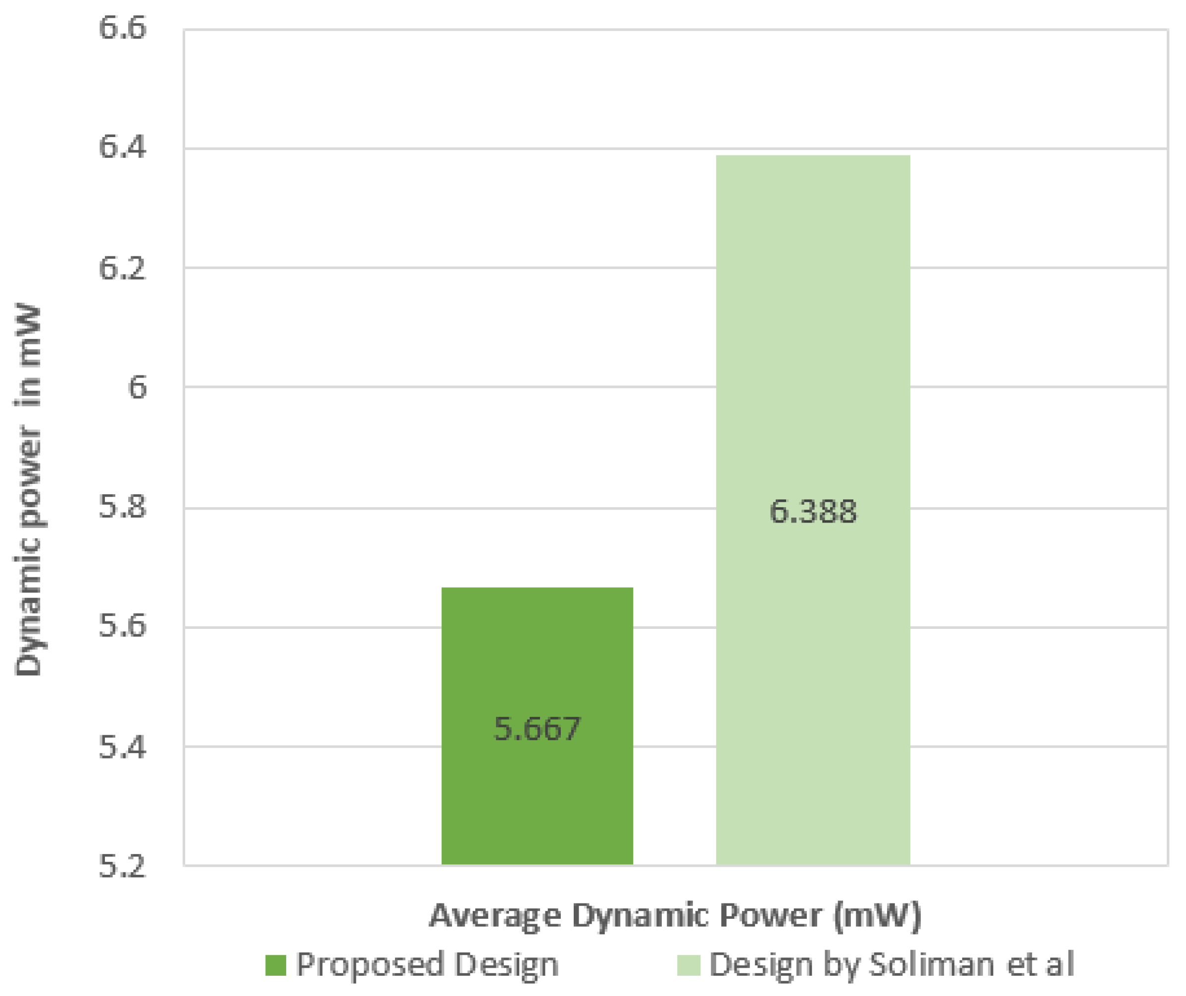
Third, the average dynamic power consumption results are exploited. The average dynamic power consumption recorded when using three cipher algorithms was 5.667 mW. On the other hand, the recorded average dynamic power consumption when utilizing five cipher algorithms similar to the state-of-the-art design in [3] was 6.388 mW. Figure 12 illustrates the average power consumption results.

Figure 12.
Average dynamic power consumption in the proposed design and the state-of-the-art design.
4.4. Results of Power Adaptive-Based Design
First, the results of the reconfiguration time are reviewed in comparison with the state-of-the-art design [7]. The state of art design [7] recorded the same reconfiguration time for all the five cipher algorithms used. Figure 13 illustrates the reconfiguration time recorded in the presented design and the state-of-the-art design.
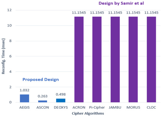
Figure 13.
Reconfiguration time in presented design and state of the art design.
The reconfiguration time decreased by at least 90% when compared with the state-of-the-art design [7].
Second, the results of the maximum resource utilization are reviewed. The maximum resource utilization recorded in the proposed design was achieved when deploying the AEGIS algorithm for maximum logic LUTs utilization and DEOXYS for the maximum memory LUT utilization. The maximum resource utilization in the state of art design was recorded when deploying the MORUS algorithm. Figure 14 reviews the maximum resource utilization results.
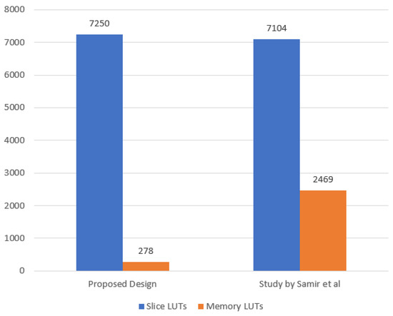
Figure 14.
Maximum resource utilization in presented design and the state of the art design.
The maximum resource utilization recorded a slight increase of about 2% in the maximum logic LUTs used in comparison with the state-of-the-art design, while a decrease of 88% was achieved in the maximum memory LUTs utilized.
Third, the average dynamic power consumption results are reviewed in comparison with the state-of-the-art design [7]. In the proposed design, the average dynamic power consumption recorded was approximately 5.667 mW. On the other hand, the state-of-the-art design recorded a 4.7 mW average dynamic power consumption. Figure 15 illustrates the average dynamic power consumption compared with the state-of-the-art design [7]. The average dynamic power consumption in the proposed design was about 10% higher in comparison with the state-of-the-art design.
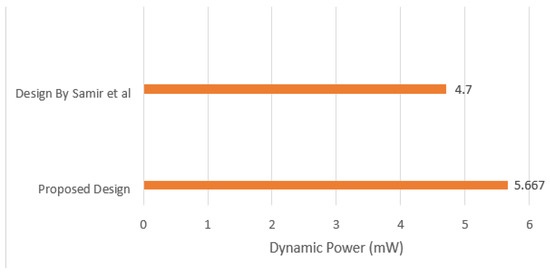
Figure 15.
Average dynamic power consumption of proposed design and state-of-the-art design.
There are a few drawbacks that did not have a substantial impact on the design such as an increase in the power consumption of the design by about 10% in the power adaptive design due to the utilization of high-performance algorithms such as AEGIS. However, the reconfiguration time decreased by at least 38% in the algorithm hopping-based design and a decrease of approximately 90% was recorded in the power adaptive-based design, which is of great significance when compared to the increased area and power.
5. Conclusions
In this work, a high-performance IoT security architecture is introduced where three lightweight cryptographic ciphers are utilized. The cipher algorithms AEGIS, ASCON, and DEOXYS-II were the finalists in the CAESAR competition in the three competition categories. The interchanging between the three ciphers is achieved by using the dynamic partial reconfiguration feature of FPGAs. Two approaches are used for the selection of the algorithms needed for FPGA reconfiguration: the algorithm hopping technique and the power adaptive technique. This work aims to enhance the reconfiguration time of FPGA by using the LZ4 compression algorithm to compress and decompress the partial bitstreams files of the cipher algorithm before reconfiguring the bit files. The proposed design shows a minimum of 38% reduction in the reconfiguration time after the inclusion of the compression/decompression. However, a slight increase in the area utilization and power consumption is recorded.
Author Contributions
Conceptualization, M.A., A.S., and M.A.A.E.G.; methodology, M.A., and A.S.; software, M.A. and A.S.; validation, M.A., and A.S.; formal analysis, M.A., and A.S.; investigation, M.A., and A.S.; resources, M.A.A.E.G.; data curation, M.A., and A.S.; writing—original draft preparation, M.A.; writing—review and editing M.A.; visualization, M.A.; supervision, M.A.A.E.G.; project administration, M.A. and A.S.; funding acquisition, N/A. All authors have read and agreed to the published version of the manuscript.
Funding
This research received no external funding.
Conflicts of Interest
The authors declare no conflict of interest.
References
- Shisha, A.; AboelMaged, M.; Aboshabaan, R.; Hassan, A.; Fouad, M.; El Ghany, M.A.A. Efficient Hardware Implementation for IoT Security System. In Proceedings of the 2020 2nd Novel Intelligent and Leading Emerging Sciences Conference (NILES), Giza, Egypt, 24–26 October 2020; pp. 204–207. [Google Scholar] [CrossRef]
- Liu, X.; Baiocchi, O. A Comparison of the Definitions for Smart Sensors, Smart Objects and Things in IoT. In Proceedings of the IEEE IEMCON 2016, Vancouver, BC, Canada, 13–15 October 2016. [Google Scholar]
- Soliman, S.; Jaela, M.A.; Abotaleb, A.M.; Hassan, Y.; Abdelghany, M.; Abdel-Hamid, A.T.; Salama, K.N.; Mostafa, H. FPGA implementation of dynamically reconfigurable IoT security module using algorithm hopping. Integr. VLSI J. 2019, ED-68, 108–121. [Google Scholar] [CrossRef]
- Bhardwaj, I.; Kumar, A.; Bansal, M. A Review on Lightweight Cryptography Algorithms for Data Security and Authentication in IoTs. In Proceedings of the 4th IEEE International Conference on Signal Processing, Computing, and Control, Solan, India, 21–23 September 2017. [Google Scholar]
- Philip, M.A. A Survey on Lightweight Ciphers for IoT Devices. In Proceedings of the IEEE International Conference on Technological Advancements in Power and Energy (TAP Energy), Kollam, India, 21–23 December 2017. [Google Scholar]
- Johnson, P.; Chakraborty, R.; Mukhopadhyay, D. A PUF-Enabled Secure Architecture for FPGA-Based IoT Applications. IEEE Trans. Multi-Scale Comput. Syst. 2015, 1, 110–122. [Google Scholar] [CrossRef]
- Samir, N.; Gamal, Y.; El-Zeiny, A.N.; Mahmoud, O.; Shawky, A.; Saeed, A.; Mostafa, H. Energy-Adaptive Lightweight Hardware Security Module using Partial Dynamic Reconfiguration for Energy Limited Internet of Things Applications. In Proceedings of the IEEE International Symposium on Circuits and Systems (ISCAS), Sapporo, Japan, 26–29 May 2019. [Google Scholar]
- Sellers, B.; Heiner, J.; Wirthlin, M.; Kalb, J. Bitstream compression through frame removal and partial reconfiguration. In Proceedings of the International Conference on Field Programmable Logic and Applications, Prague, Czech Republic, 31 August–2 September 2009; pp. 476–480. [Google Scholar] [CrossRef]
- Bartík, M.; Ubik, S.; Kubalík, P. LZ4 Compression Algorithm on FPGA. In Proceedings of the IEEE International Conference on Electronics, Circuits, and Systems (ICECS), Cairo, Egypt, 6–9 December 2015. [Google Scholar]
- CAESAR. Competition. 2014. Available online: https://competitions.cr.yp.to/caesar-call.html (accessed on 1 February 2021).
- Katsaiti, M.; Sklavos, N. Implementation Efficiency and Alternations, on CAESAR Finalists: AEGIS Approach. In Proceedings of the 2018 IEEE 16th Intl Conf on Dependable, Autonomic and Secure Computing, 16th Intl Conf on Pervasive Intelligence and Computing, 4th Intl Conf on Big Data Intelligence and Computing and Cyber Science and Technology Congress (DASC/PiCom/DataCom/CyberSciTech), Athens, Greece, 12–15 August 2018; pp. 661–665. [Google Scholar] [CrossRef]
- Wu, H.; Preneel, B. AEGIS: A Fast-Authenticated Encryption Algorithm Submission to the CAESAR Competition. 2016. Available online: https://competitions.cr.yp.to/caesar-submissions.html (accessed on 1 February 2021).
- Dobraunig, C.; Eichlseder, M.; Mendel, F.; Schläffer, M. ASCON v.1.2 Submission to the CAESAR Competition. 2016. Available online: https://competitions.cr.yp.to/caesar-submissions.html (accessed on 1 February 2021).
- Setetemela, K.O.; Keta, K.; Nkhabu, M.; Winberg, S. Python-based FPGA Implementation of AES using Migen for Internet of Things Security. In Proceedings of the IEEE 10th International Conference on Mechanical and Intelligent Manufacturing Technologies (ICMIMT), Cape Town, South Africa, 15–17 February 2019. [Google Scholar]
- Jean, J.; Nikoli´c, I.; Peyrin, T.; Seurin, Y. DEOXYS v1.41 Submission to CAESAR Competition. 2016. Available online: https://competitions.cr.yp.to/caesar-submissions.html (accessed on 1 February 2021).
- Kumar, K.A.A. A secure frequency hopping synthesizer for reconfigurable wireless radios. In Proceedings of the 2013 IEEE Conference on Information & Communication Technologies, Thuckalay, Tamil Nadu, India, 11–12 April 2013; pp. 851–854. [Google Scholar] [CrossRef]
- Xilinx Inc. Partial Reconfiguration User Guide, User Guide 702, v. 14.5. 2013. Available online: https://www.xilinx.com/support/documentation/sw_manuals/xilinx14_7/ug702.pdf (accessed on 5 February 2021).
- Vipin, K.; Fahmy, S.A. FPGA Dynamic and Partial Reconfiguration: A Survey of Architectures, Methods, and Applications. ACM Comput. Surv. 2018, 51, 1–39. [Google Scholar] [CrossRef] [Green Version]
- Kamaleldin, A.; Ahmed, I.; Obeid, A.M.; Shalash, A.; Ismail, Y.; Mostafa, H. A Cost-Effective Dynamic Partial Reconfiguration Implementation Flow for Xilinx FPGA. In Proceedings of the 2017 New Generation of CAS (NGCAS), Genova, Italy, 6–9 September 2017; pp. 281–284. [Google Scholar] [CrossRef]
- Kamaleldin, A.; Mohamed, A.; Nagy, A.; Gamal, Y.; Shalash, A.; Mostafa, H. Design Guidelines for the High-Speed Dynamic Partial Reconfiguration Based Software Defined Radio Implementations on Xilinx Zynq FPGA. In Proceedings of the IEEE International Symposium on Circuits and Systems, Baltimore, MD, USA, 28–31 May 2017. [Google Scholar]
- Xilinx Inc. AXI HWICAP PG134 (Oct. 2016). 2016. Available online: https://www.xilinx.com/support/documentation/ip_documentation/axi_hwicap/v3_0/pg134-axi-hwicap.pdf (accessed on 5 February 2021).
- Dye, D. Partial Reconfiguration of Xilinx FPGAs Using ISE Design Suite, WP374 (v1.2), Xilinx. 2012. Available online: https://www.xilinx.com/support/documentation/white_papers/wp374_Partial_Reconfig_Xilinx_FPGAs.pdf (accessed on 5 February 2021).
- Yann Collet. Real Time Data Compression: Development Blog on Compression Algorithms: LZ4. Available online: http://fastcompression.blogspot.com/p/lz4.html (accessed on 5 February 2021).
- Liu, W.; Mei, F.; Wang, C.; O’Neill, M.; Swartzlander, E.E. Data Compression Device Based on Modified LZ4 Algorithm. IEEE Trans. Consum. Electron. 2018, 64, 110–117. [Google Scholar] [CrossRef] [Green Version]
- Yann Collet. Real Time Data Compression: Development Blog on Compression Algorithms: LZ4 Explained. Available online: http://fastcompression.blogspot.com/2011/05/lz4-explained.html (accessed on 5 February 2021).
- Datta, D.; Datta, B.; Dutta, H.S. Design and implementation of multibit LFSR on FPGA to generate pseudorandom sequence number. In Proceedings of the 2017 Devices for Integrated Circuit (DevIC), Kalyani, Nadia, 23–24 March 2017; pp. 346–349. [Google Scholar] [CrossRef]
- Homsirikamol, E.; Diehl, W.; Ferozpuri, A.; Farahmand, F.; Sharif, M.U.; Gaj, K. GMU Hardware API for Authenticated Ciphers. In Proceedings of the International Conference on Reconfigurable Computing and FPGAs, Riviera Maya, Mexico, 13–15 December 2015; pp. 1–8. [Google Scholar]
- Kilts, S. Advanced FPGA Design Architecture, Implementation, and Optimization; Wiley-Interscience: Hoboken, NJ, USA, 2007; pp. 83–94. [Google Scholar]


Publisher’s Note: MDPI stays neutral with regard to jurisdictional claims in published maps and institutional affiliations. |
© 2021 by the authors. Licensee MDPI, Basel, Switzerland. This article is an open access article distributed under the terms and conditions of the Creative Commons Attribution (CC BY) license (https://creativecommons.org/licenses/by/4.0/).