Article

New EV Battery Charger PFC Rectifier Front-End Allowing Full Power Delivery in 3-Phase and 1-Phase Operation

Power Electronic Systems Laboratory, ETH Zürich, 8092 Zurich, Switzerland
*
Author to whom correspondence should be addressed.
Electronics 2021, 10(17), 2069; https://doi.org/10.3390/electronics10172069
Submission received: 23 July 2021 / Revised: 17 August 2021 / Accepted: 18 August 2021 / Published: 26 August 2021
(This article belongs to the Section Power Electronics)

Abstract

:
A new universal front-end PFC rectifier topology of a battery charger for Electric Vehicles (EVs) is proposed, which allows fast charging at rated and/or full power level in case of 3-phase (Europe) as well as 1-phase (USA) mains supply. In this regard, a conventional 3-phase PFC rectifier would facilitate only one-third of the rated power in case of 1-phase operation. The new topology is based on a two-level six-switch (2LB6) 3-phase boost-type PFC rectifier, which is extended with a diode bridge-leg and additional windings of the Common-Mode (CM) chokes of the EMI filter. Besides this extension of the power circuit, the general design of the new converter is explained, and the generated Differential Mode (DM) and Common Mode (CM) EMI disturbances are investigated for 3-phase and 1-phase operation, resulting in guidelines for the EMI filter design. The EMI performance (CISPR 11 class-B QP) is experimentally verified for 1-phase and 3-phase operation at an output power of 4.5 kW, using a full-scale hardware prototype that implements the proposed extensions for a 2LB6 3-phase boost-type PFC rectifier and that is designed for output power levels of 22 kW and 19 kW in case of 3-phase and 1-phase operation, respectively. Compared to a conventional 2LB6 PFC rectifier, the volume of the extended system increases from 2.7 dm 3 to 3.4 dm 3 , of which 0.5 dm 3 is due to the additional dc-link capacitance for buffering the power pulsation with twice the mains frequency occurring for 1-phase operation.

1. Introduction

The internationally increasing sales figures of Electric Vehicles (EVs) results in a demand for universal front-end PFC rectifier topologies of EV chargers that facilitate full power operation in presence of 3-phase and 1-phase mains. For example, in Europe, a charging power of 22 kW is accessible from the 3-phase mains with a line-to-line rms voltage of 400 V and a maximum phase current of 32 A [1]. In the USA, the three-wire split-phase system, which basically represents a 1-phase mains, provides similarly high power of 19.2 kW with an rms voltage of 240 V and a maximum current of 80 A [2].
In the context of economy of scale, it can be preferable that both, i.e., 3-phase and 1-phase operation, are covered using the same power circuit, especially a universal ac/dc front-end. Different reasons for potential cost reductions are listed below.
  • Reduced development effort since only a single product needs to be designed and tested.
  • Product certification, e.g., as described in [3], which often is a time-consuming process for automotive supply equipment, needs to be conducted for only one product instead of two.
  • Reduction of the number of different components, in particular magnetic components.
  • Only a single production line is needed to manufacture the EV charger.
For these reasons, it is expected that, up to a certain production volume, the total cost of the presented converter structure is lower than the total cost of two separate EV chargers (in case of very high production volumes, a lower total cost may be achieved with separate EV chargers for 3-phase and 1-phase operation, as a separate realization facilitates the independent optimization with regard to the specific requirements).
A straightforward realization can be achieved with three individual 1-phase PFC ac/dc converter modules, as described, e.g., in [4,5,6,7], which requires three individual isolated dc/dc converters. Alternatively, according to Figure 1a, the front-end of an EV charger (which comprises an ac/dc converter and a dc/dc converter with galvanic isolation [8]) can be realized with a conventional 3-phase boost-type PFC rectifier that readily enables 1-phase operation, cf. Figure 1b, whereas the unused bridge-leg, e.g., of phase b in Figure 1b, can be employed to buffer the Low-Frequency (LF) power pulsation at the dc-link, as detailed in [9]. However, the maximum power in case of 1-phase operation is limited to approximately one-third of the nominal 3-phase power, as the power components of the rectifier stage in each phase are only rated for the current occurring for nominal 3-phase operation [10,11].
These state-of-the-art approaches are the starting point for investigating whether a conventional 3-phase PFC rectifier can be extended such that 1-phase operation is feasible at full power. This potentially offers advantages concerning circuit complexity, realization effort, and manufacturing costs. The resulting PFC rectifier has been introduced in [12]. In the following, a systematic design procedure is presented, based on a detailed stress comparison, between the two types of operation. Furthermore, the guidelines for the EMI filter design in [12] are further developed, including FEM simulations for each of the proposed realizations of the 4-phase CM choke, as well as, experimental measurements. Finally, a full-scale hardware prototype allows for experimental verification, revealing the viability of the proposed concept.
To start with, Section 2 describes the extension of a 3-phase two-level six-switch (2LB6) PFC rectifier topology with respect to full power 1-phase operation. The proposed extension can also be applied to multilevel 3-phase ac/dc converters whose power stages do not require a connection to the dc-link midpoint (e.g., a flying capacitor converter). Section 3 details the design of the power circuit, i.e., the derivation of the analytical expressions used to calculate the component stresses and presents a design guideline, which clarifies specific design requirements. Section 4 investigates conducted EMI in case of 3-phase and 1-phase operation. The EMI equivalent circuits derived in this context enable the identification of most critical operating conditions (3-phase or 1-phase) for Differential Mode (DM) and Common Mode (CM) disturbances and facilitate the compilation of guidelines for the EMI filter design. Section 5 presents the experimental verification of the theoretical considerations at an output power of 4.5 kW, using a full-scale hardware prototype that implements the proposed extensions for a 2LB6 3-phase boost-type PFC rectifier. The measurement results confirm that the EMI filter complies with CISPR 11 Class-B QP regulations in case of 3-phase and 1-phase operation.

2. Modifications for 1-Phase Operation

This Section summarizes the three extensions that are applied to the 2LB6 3-phase PFC rectifier depicted in Figure 1, in order to gain 1-phase operating capability at full power. Starting from the power stage, these are listed below.
  • Dc-side unfolder (passive diode bridge-leg) for the return current.
  • Dc-side relay to enable dc-side CM filtering with a CM filter capacitor for 1-phase and 3-phase operation.
  • Modified EMI filter: 4-phase CM chokes; no CM chokes in the filter stages directly connected to the switching stage.
Figure 2 depicts the resulting converter topology. A detailed explanation is presented in [12].
Table 1 lists the main converter specifications, which reveal similar output power levels and similar phase voltages in case of 3-phase and 1-phase operation. Accordingly, similar component stresses are expected for the two modes of operation. The three half-bridges of the PFC rectifier can be operated in parallel during 1-phase operation in order to equally share the mains current, advantageously with interleaving, which, however, requires all three phases—a, b, and c—of the rectifier for drawing the input current. Therefore, the 3-phase PFC rectifier needs to be equipped with a conductor for the return current. This conductor could be directly connected to the dc-link midpoint, O, in Figure 1. However, this solution would lead to very high dc-link capacitances, as both the upper and the lower dc-link capacitors would only be charged during every second mains half cycle in an alternating manner. For this reason, the rectifier is extended by a passive diode bridge-leg that is realized with low-cost Si diodes and acts as unfolder. Compared to the direct connection to the dc-link midpoint, the LF RMS current of the dc-link reduces from 44 A to 18 A. The return conductor is connected to the ac input of this unfolder bridge-leg as shown in Figure 2. The resulting topology resembles a typical interleaved totem pole PFC rectifier [13].
In the 2LB6 3-phase PFC rectifier shown in Figure 1, the star-point formed with the DM EMI filter capacitors is connected back to the midpoint, O. This connection enables a low-impedance current path for CM EMI disturbances and stabilizes the electric potential of the midpoint with respect to earth at high frequencies [14,15]. In addition, one or more CM EMI filter capacitors can be installed at the dc side, e.g., between O and PE, in order to further decrease the level of CM EMI noise applied to the EMI filter [16]. However, during 1-phase operation, the rectifier diodes of the unfolder change their states at every zero-crossing of the phase current. The voltage between O and PE, v O , PE , can be determined based on the voltage loops I and II depicted in Figure 3. Depending on the conducting diode, i.e., D 1 or D 2 , loop I or II is valid, respectively. Therefore, should the voltage drop across the EMI filter be neglected at mains frequency,
v O , PE v ac ( t ) / 2 V dc / 2 i ac < 0 ( loop I ) , v ac ( t ) / 2 + V dc / 2 i ac > 0 ( loop II ) .
Results. According to (1), v O , PE is subject to a voltage step of V dc at every zero-crossing of the phase current, cf. Figure 2, which leads to an increase of the EMI noise floor, e.g., as described in [17,18]. For this reason, no filter capacitor should be connected between O and PE in 1-phase operation. However, as the voltage between the midpoint of the unfolder, O’, and earth, is not subject to such voltage step, v O , PE v ac / 2 , a filter capacitor, C cm 0 , can be placed between O’ and PE to attenuate CM EMI noise. Accordingly, a relay is installed between O and O’, which is in the on-state during 3-phase operation and in the off-state during 1-phase operation in order to keep C cm 0 effective for 3-phase and 1-phase operation.
In a last step, the EMI filter needs to be modified, which, in particular, requires the 3-phase CM chokes to be extended. These CM chokes are intended to handle a small magnetizing current, because the sum of the phase currents, i a + i b + i c , is approximately zero during 3-phase operation. However, during 1-phase operation the sum of the phase currents is equal to the return current and the cores of the 3-phase CM chokes would saturate. Accordingly, all CM chokes must feature a 4th winding for the return current. Figure 4a depicts a straightforward realization of this CM choke with a single 4th winding. This construction is cost-effective because it requires only four dedicated windings but it introduces an asymmetry that can be critical regarding mixed-mode EMI noise [19,20]. An assessment of the implications of this asymmetry on the components’ stray inductances is presented in Appendix A for a selected design example, for which an acceptable ratio of 1.41 for maximum to minimum stray inductance is obtained. Apart from that, the construction of Figure 4a enables a PCB layout that is of low complexity and features a high fill factor, as it requires a minimum number of separators between the windings. A more symmetric construction is depicted in Figure 4b where the 4th winding is split up into three parts that are connected in series. This construction is more complex to realize than that of Figure 4a and limited to numbers of turns that are a multiple of three. Both constructions have in common that the cross section of the wire of the 4th winding is three times larger than that of each wire of the three phases. With this, same LF winding losses occur during 1-phase operation in all four windings. Initially, it was intended to realize both CM chokes based on the more symmetric construction depicted in Figure 4b; however, it turned out that the construction with a single 4th winding features a lower number of connections and enables a PCB layout with less overlapping conductors. Thus, lower parasitic capacitances due to interconnections result. In order to verify the proper operation of both configurations, L cm 3 is based on Figure 4b and L cm 4 on Figure 4a.
Finally, the filter stages directly connected to the switching stage, e.g., the 1st filter stage, do not comprise a CM choke, cf. Figure 2. The reason is that a 4-phase CM choke, during 3-phase operation (where the relay is in the on-state), would short circuit the zero sequence voltage inherently generated by the 2LB6 topology. Instead of that, the CM choke is placed close to the mains-side interface of the EMI filter where it is fully effective, i.e., L cm 4 in Figure 2. Furthermore, in anticipation of the detailed analytical investigation conducted in Section 4, a second CM choke is placed in the 3rd filter stage ( L cm 3 ), together with a CM EMI filter capacitor between the two CM chokes.
The DM part of the EMI filter can remain unchanged because the DM EMI filter components are similarly effective for both 3-phase and 1-phase operation. The DM filter components L dm 2 / 3 and L dm 1 / 3 in the return path are only used for the reason of symmetry and could be omitted.
The presented extension can be applied to any conventional multilevel 3-phase ac/dc converter that can be implemented without connection to the dc-link midpoint (e.g., a flying capacitor converter). A possible extension of ac/dc converters with inherent utilization of the midpoint (e.g., T-type converter) is presented in Appendix C.

3. Design of Main Power Stage

This section aims for a systematic design of the converter that takes into consideration whether 3-phase or 1-phase operation is more critical for the design of a power component. In this regard, suitable values of switching frequency and inductor current ripple are determined in Section 3.1, and the selection or design of the power components is presented in Section 3.2. The expressions used to calculate the currents in the power components and the losses for 3-phase and 1-phase operation are well known; for the reason of completeness, the expressions used in the course of the converter design are compiled in Appendix B.

3.1. Switching Frequency and Current Ripple

In order to obtain a compact EMI filter, it is sufficient to limit the switching frequencies that are considered during the design process to a set of discrete values, f s { 24 , 36 , 48 , 72 , 144 } kHz [21]. From these, f s = 48 kHz has been considered, as this choice provides acceptable switching losses and a compact design of the boost inductor [22,23].
The value of the current ripple has been determined such that, in case of 1-phase operation, the diode bridge-leg is not subject to parasitic HF switching operations around the zero crossing of the phase current, due to the superimposed HF ripple. As the three phases are modulated with interleaved carriers during 1-phase operation, the HF ripple of the current in the rectifier diodes only contains harmonic components at 3 f s and multiples thereof (cf. Section 4). Furthermore, the superimposed HF ripple leads to a total current in the return path that is limited by an upper and a lower envelope. In our case, the lower envelope is of interest, because it enables the derivation of a condition for L 1 such that parasitic HF oscillations of the diode bridge-leg ac-side voltage are avoided. The expression for the lower envelope of the return current can be estimated with the mains current fundamental component and the amplitude of the spectral component at 3 f s , calculated from the Fourier series of the rectangular waveform of the switch-node voltage,
i D , env ( t ) = 2 P V ac , rms sin ( 2 π f m t ) LF term V dc 9 f s L 1 3 π 2 sin ( 3 π d ( t ) ) ampl . of spectral comp . at 3 f s . .
According to (2), parasitic HF switching of the diode bridge-leg is avoided if the gradient of the LF term is greater than the gradient of the amplitude of the 3rd harmonic at t 0 . For output power levels greater than 2.5 kW, this condition leads to L 1 = 150 μ H , which translates into a peak-to-peak current ripple of 60%. In case the specifications require operation at lower power, low-power MOSFETs or IGBTs can be placed in parallel to the diodes, to clamp the path of the current around zero-crossings.

3.2. Power Components

Using the provided expressions of Appendix B all currents can be calculated for 3-phase and 1-phase operation; Table 2 lists the obtained results. The comparison of the listed values reveals slightly higher values of I ph , rms and I ph , avg in case of 3-phase operation, which is due to the higher output power of 22 kW. However, 1-phase operation leads to a higher peak value of the phase current and a higher HF rms value of the inductor current, as the durations with large current ripples are longer than for 3-phase operation. Furthermore, the dc-link capacitors are subject to high LF rms currents during 1-phase operation. These results, in combination with (A6), (A10), and (A33), allow to directly draw the conclusion that 3-phase operation is more relevant for the selection of the MOSFETs and 1-phase operation is important for the design of the dc-link capacitor. The selected power components are listed in Table 3. A single 1EDI60N12AF gate driver (by Infineon) is employed for each pair of parallel MOSFET devices with separate gate resistors. Moreover, for the relay on the dc-side (cf. Section 2), two parallel IM06DGR relays from TE have been employed. Such configuration is possible, as the relays are only used as disconnectors and are not intended to switch any current. (In case interoperability is not considered, i.e., possibility of operation in Europe and in the USA, the relay can be omitted (1-phase operation) or replaced by a hardwired connection (3-phase operation)).
With regard to the design of the boost inductor, both operating modes need to be considered, as 3-phase operation leads to higher copper losses (higher value of I ph , rms ) and 1-phase operation causes higher core losses and is more critical with regard to a saturation of the magnetic core (higher values of I ph , pk and I L ph , rms , HF ). In order to ensure that the defined values for peak flux density and current density are maintained, the area product of (A12) is modified,
( A c A w ) min = max L 1 I ph , pk B pk max I ph , rms k f J rms .
In order to evaluate (3), the values for B pk and J rms need to be defined. With regard to the current density, a typical value of J rms = 4 A / mm 2 is used. However, the value of the peak flux density depends on the selected core material. In this work, the core of the boost inductor is made of the iron powder material KoolMu, as this features a compact design, due to a high useful flux density, and a smooth transition to saturation in case of overcurrent conditions. However, the practically useful peak flux density is lower than the material’s saturation flux density of 1 T, as the permeability of the material and, with this, the resulting inductance decrease for increasing magnetic flux density. Therefore, B pk 500 mT is used, which, for the finally chosen material with an initial relative permeability of μ r = 60 , tolerates a decrease to μ r = 26 . With this, ( A c A w ) min = 23 cm 4 results. This area product serves as initial value for selecting a suitable core. The final inductor design is conducted with the multi-domain inductor optimization algorithm outlined in [24] that takes nonlinear effects and coupled electro-thermal effects into account and results in an area product of 25.2 cm 4 . Table 4 lists the resulting inductor design. This inductor design features an initial inductance of 170 μ H at zero current and tolerates a decrease of the inductance to 100 μ H at 45 A (the maximum of the LF phase current in case of 3-phase operation) and 80 μ H at 57 A .
Table 5 summarizes the estimated losses for all main power components and for 3-phase and 1-phase operation. The sum of all semiconductor losses is 214 W for 3-phase operation and 239 W for 1-phase operation, due to the additional losses in the diodes. Therefore, the cooling system is dimensioned based on 1-phase operation. For the cooling system, a pin-fin heat sink design is considered, which is known to outperform conventional plate-fin heat sinks [25]. The selection of the heat sink has been a two-step process. First, an online tool that considers lateral airflow [26] has been used to pre-select a suitable heat sink. In a second step, the thermal resistance of the cooling system (comprised of the selected heat sink and the fans used for the final system) has been measured in the course of an experiment, in order to ensure that the achieved thermal resistance is sufficiently small. The calculated losses for the boost inductor reveal a slightly higher value of 92 W in case of 1-phase operation compared to 80 W for 3-phase operation, which is due to substantially higher HF copper and core losses. With the additional losses in the dc-link capacitor of 15 W, the estimated total losses for 1-phase operation are 339 W and, with this, approximately 15 % higher than the estimated total losses for 3-phase operation (294 W). (Consideration of the conduction losses of the EMI filter further extends the losses difference between the two operating modes, due to the additional current in the return path.) This increase of the losses can be lowered by reducing the dc-link voltage, e.g., to 1 2 × 750 V , which is in principle feasible, because the maximum swing of the input voltage applied to the active bridge-legs of the rectifier reduces from 2 × 2 × 230 V = 650 V for 3-phase operation to 2 × 240 V = 340 V for 1-phase operation. However, for this, the system needs to be further extended, which includes two output-side dc-dc converters with galvanic isolation. The respective modifications and possible loss reductions are explained in Appendix B.3.
Figure 5a,b depicts simulated waveforms for 3-phase and 1-phase operation, respectively. The circuit simulations have been used to verify the component stresses calculated in this Section. It can be seen that the dc-link voltage shows a peak-to-peak voltage ripple of 42 V in 1-phase operation, due to the power pulsation with twice the mains frequency. (In the final EV charger application, the realized ac/dc converter will be connected to a dc/dc converter stage with galvanic isolation, which continuously adapts to the changing dc-link voltage and provides a constant output voltage [27]).

4. Generated EMI Noise and Filtering

This section provides individual analyses of the EMI noise components that occur in case of 3-phase and 1-phase operation. According to the work in [28], the peak EMI noise levels measured with a test receiver that complies with the CISPR 16 regulation, e.g., featuring a receiver bandwidth (RBW) of 9 kHz, can be approximated with
max noise ( f ) = 20 log 10 1 1 μ V ξ = f RBW 2 ξ = f + RBW 2 V sim ( ξ ) ,
where V sim ( ξ ) denotes the spectrum of the simulated voltage at the HF output of the Line Impedance Stabilization Network (LISN), which is terminated with a resistance of 50 Ω . The time interval of the simulation is equal to a single mains period. In the following, (4) is used to determine the DM and the CM components of the EMI noise.

4.1. Conducted EMI for 3-Phase Operation

In case of 3-phase operation, the relay contact in Figure 2 is closed. With this, the HF EMI model shown in Figure 6a results. The EMI noise source is modeled with one CM source and three DM sources:
v cm = v AO + v BO + v CO 3 ,     v dm , i = v i O v cm i { A , B , C } .
Furthermore, Figure 6a considers the three parasitic capacitances C par , sw between the switch-nodes and PE, because these capacitances are found to have a substantial impact on the effective CM attenuation of the EMI filter. (Due to the grounded heat sink, the value of C par , sw can be approximated by the total surface of the metallic backplates of the low-side MOSFETs and the thickness and the permittivity of the interface material [29,30], which for two parallel MOSFETs (TO-247 packages) per switch leads to 3 C par , sw = 225 pF ).
For the design of the DM part of the filter, each stage of the DM filter, k, is considered to achieve an attenuation of
Att k , dB = 20 log 10 ( ω 2 C k L k ) ,
for frequencies much greater than the corner frequency. The dashed red line in Figure 6a highlights a path of HF DM EMI noise.
The CM part of the EMI filter is commonly assessed with the equivalent circuit for EMI CM noise depicted in Figure 6b. The respective derivation of the CM EMI model is conducted in the style of the works in [31,32]. In a first step, the first filter stage is considered, which is not symmetric, i.e., the inductor L 1 / 3 is only present in the upper vertical path; the lower vertical path of the first filter stage does not contain a filter component. For this reason, the CM noise current will prefer the lower path of the first filter stage and L 1 / 3 can be replaced by an open circuit. Furthermore, the capacitance 3 C 1 features a very low impedance for the CM noise current and is approximated by a short circuit. Moreover, the CM noise source can be replaced by its Thévenin equivalent source, cf. Figure 6c, with
C eq = 3 C par , sw + C par , dc + C cm 0 ,
v cm , par = v cm 3 C par , sw C eq .
According to (7) and (8), the effective CM noise voltage, v cm , par , can be decreased by increasing the value of C cm 0 . However, the impedance between the voltage source v cm , par and the CM equivalent circuit of the EMI filter decreases for increasing value of C cm 0 , too. A respective analysis reveals that, due to the high CM impedance of L cm 3 in the considered frequency range, f [ 150 kHz , 30 MHz ] , even the parasitic capacitances 3 C par , sw + C par , dc feature a sufficiently low impedance such that C eq | C cm 0 0 can be approximated by a short circuit for f > 400 kHz . Based on this consideration, Figure 6c can be further simplified to the structure depicted in Figure 6d, which, together with (8), reveals the increase of the CM attenuation for an increasing capacitance of C cm 0 and highlights the impact of the remaining EMI filter components, L cm 3 , C cm 3 , and L cm 4 , on the CM attenuation of the EMI filter.

4.2. Conducted EMI of 1-Phase Operation

The DM equivalent circuit is depicted in Figure 7a. Due to the interleaved modulation of the three active bridges of the PFC rectifier, ideally, only the multiples of the switching frequency that are equal to ( 3 k + 3 ) f s , k N 0 , are relevant as they are common to all three phases and appear in the LISN; the remaining HF harmonics do not lead to significant voltages at the LISN.
The equivalent circuit for filtering the relevant spectral components at ( 3 k + 3 ) f s , depicted in Figure 7b, is similar to Figure 6b, except that the neutral conductor is also connected to the LISN. As the parallel current path through C cm 0 and C cm 3 is ineffective (because the magnetizing inductances of L cm 3 and L cm 4 become effective in case of such a current), the effective DM EMI filter is composed of the DM filter components and the stray inductances of L cm 3 and L cm 4 . The circuit of Figure 7b serves for the evaluation of DM EMI noise in 1-phase operation.
With regard to the CM EMI noise in 1-phase operation, two main sources are identified. First, the LF switching of the mains rectifier diodes causes CM EMI noise, which is greatly reduced by proper placement of C cm 0 . The second source of CM noise is the effective switched voltage, v dm , ( 3 k + 3 ) , k N 0 , that generates displacement currents through the parasitic capacitances, C par , sw . The derivation of the equivalent filter circuit is identical to that of 3-phase operation presented in Section 4.1, cf. Figure 7c–e, only that the load resistance is different, i.e., R LISN / 2 instead of R LISN / 3 .

4.3. Basic Design Guideline for the EMI Filter

The design of the EMI filter is a three-step procedure. In a first step, DM and CM attenuations required for 3-phase and 1-phase operation are determined in order to identify the most critical mode of operation. Thereafter, the number of filter stages for the calculated attenuation is defined. With this information, the components of the EMI filter can be designed in a last step.
For the investigated EMI filter, the number of filter stages for attenuating DM and CM EMI noise has been set to n dm = 3 and n cm = 2 , respectively. These are typical values that are commonly used for PFC rectifiers with similar specifications [33].
According to the discussion presented in Section 4.1 and Section 4.2, the four networks depicted in Figure 6a,d and Figure 7b,e need to be considered in order to assess whether 3-phase or 1-phase operation is more critical with respect to the required DM and/or CM attenuation. The noise voltages are calculated for each equivalent circuit, based on (4). The spectra of the noise voltages feature envelopes that decrease with a slope of at least 20 dB/dec, and each L-C-filter stage of the EMI filter ideally provides an attenuation that increases with 40 dB/dec in the relevant frequency range. In addition, the specified spectrum of allowable conducted EMI emissions decreases with 20 dB/dec for 150 kHz < f < 500 kHz . For these reasons, the first significant spectral component that enters this frequency range is found to be most critical with regard to the required attenuation of the EMI filter (3-phase and 1-phase operation, as well as DM and CM noise, must be considered separately, as different EMI models apply). Table 6 lists the obtained relevant spectral components. As interleaved PWM carriers are used in case of 1-phase operation, the corresponding relevant harmonic components result at 288 kHz instead of 192 kHz. Due to this, and because the levels of the two DM voltage components are nearly equal for 3-phase and 1-phase operation ( 162 dB μ V vs. 162.3 dB μ V ), it is found that 3-phase operation, i.e., the network of Figure 6a, is decisive for the design of the DM filter, leading to a minimum required attenuation of the DM EMI noise of
Att dm , min , dB ( 192 kHz ) = ( 162 dB μ V 64 dB μ V ) + 18 dB = 116 dB ,
The additional safety margin of +18 dB accounts for an approximately 50% inductance drop of the inductors L 1 and L dm 3 at peak current, due to the employed magnetic powder cores, i.e., 12 dB of attenuation, plus approximately 6 dB for further component tolerances. With this, a rather conservative safety margin is considered.
A different result is obtained for the CM components, as the CM noise voltage for 3-phase operation is substantially less than for 1-phase operation ( 118 dB μ V vs. 126 dB μ V ). Thus, 1-phase operation, i.e., the network of Figure 7e, is found to be relevant for the design of the CM filter. Accordingly, the minimum attenuation of the CM EMI noise is
Att cm , min , dB ( 288 kHz ) = ( 126 dB μ V 60 dB μ V ) + 7 dB = 73 dB ,
which considers component tolerances.
Furthermore, certain practical aspects are considered in the course of the filter design. In this context, the attenuations of the different filter stages are partitioned such that smaller filter components with improved HF performances, i.e., with self-resonance frequencies that are deep in the MHz range, are located towards the mains. With regard to the DM filter, the attenuations at 192 kHz are set to 67 dB, 25 dB, and 18 dB for the 1st, 2nd, and 3rd filter stage, respectively. With this, a better HF performance of the EMI filter can be achieved, because a decreased attenuation of a filter stage reduces the required values of inductance and capacitance, which results in smaller components that feature improved HF properties. The final values of the EMI filter components have been optimized to minimize the total volume. (The final attenuation of stage three is 25 dB, due to the stray inductance of the subsequent CM choke, L cm 3 .) With the capacitances that result from the volume optimization of the DM filter, the total reactive power consumption does not exceed 770 VA (3.5% of 22 kW) at 50 Hz, and this is below the typical limit of 5% to 10% of the rated power [34,35]. With regard to the CM filter, the attenuation of the first filter stage, composed of L cm 3 and C cm 3 , is set to 38 dB at 288 kHz, and the attenuation of the second filter stage, i.e., L cm 4 and R LISN / 2 , to 35 dB. With L cm 4 , the EMI filter features increased CM impedance at the interface to the mains such that the filter effectively attenuates CM noise also in presence of the relatively low effective resistance of the LISN of 16.7 or 25 , cf. [16,33]. With regard to the CM filter capacitances, two considerations have been taken into account, i.e., the maximum total capacitance to PE, C cm 0 + C cm 1 , is limited by reason of the maximum allowable touch current and the ratio of C cm 3 / C cm 0 has been optimized to achieve maximum CM attenuation for a given value of L cm 3 . The filter components have been selected such that the EMI regulations are fulfilled and stable operation is achieved without the need of damping networks, to avoid increased costs due to the additional components.
The resulting filter component values are listed in Table 7. As a result of this design approach, the switching frequency is located between the resonance frequencies of stages two and three of the DM filter, cf. Figure 8a. For this reason, L dm 2 employs a ferrite N97 core, in order to maintain a constant inductance with respect to the inductor current, to avoid that the resonance frequency of the second stage approaches the switching frequency. The DM filter inductors L dm 3 and, in the return path, L dm 3 / 3 are realized with cores made of iron-powder (KoolMu), to achieve low inductor volumes. The DM filter capacitors are film capacitors that feature low losses at 50 Hz. Nevertheless, their parasitic equivalent series inductance (ESL) can be critical in terms of EMI performance and needs to be considered.
The CM filter chokes employ cores made of nanocrystalline material that features very high permeability. However, the permeability decreases with increasing frequency. For this reason, the permeability at the relevant frequency of 288 kHz has been used to design the CM choke. Furthermore, each CM choke can be subject to local saturation of the core, due to the DM currents, which causes a reduction of the CM inductance for increasing power [36]. However, a respective analysis reveals that the total peak flux density in the core, due to CM and DM currents, is only 250 mT, i.e., well below the saturation flux density of the material of 1 T. Accordingly, the designed CM chokes are found to be rather thermally limited by the LF copper losses (only these are relevant, as L cm 3 and L cm 4 are subject to relatively low HF excitations) than by the flux density.
The design of the PCB is conducted according to commonly known design guidelines [16,37,38]. The position and the orientation of each filter component has been carefully selected to minimize magnetic and/or capacitive couplings. In addition, no copper planes are present below the magnetic components and the input and output terminals of the CM chokes do not overlap.
Table 6 shows the achieved attenuations for all sources. As expected, the rms value of the noise voltage generated by v dm , ( 3 k + 3 ) (line 3 in Table 6) is highly attenuated such that the corresponding filtered noise amplitude is well below the regulated limits, which is addressed to the interleaved operation and the additional DM inductors in the return path that are present to provide symmetry (the total boxed volume of these DM inductors is 42 cm 3 or 1.2 % of the overall converter volume).
Figure 5c,d depicts the simulated spectra of the conducted EMI, which verify the validity of the presented analytic considerations (“max. noise” in Figure 5c,d denotes the maximum estimation according to (4)). In addition, the absence of frequency multiples equal to { 3 k + 1 , 3 k + 2 }, k N 0 , in 1-phase operation is depicted.

4.4. Experimental Evaluation of the EMI Filter

The transfer function of the ideal DM part of the filter (line-to-neutral), i.e., frequency-independent capacitors and inductors without parasitic components, for 3-phase operation is shown with the dashed line in Figure 8a for f [ 1 kHz , 30 MHz ] . In the same figure, the solid black line depicts the transfer function of the filter as calculated with the individually measured impedance characteristics of each component, using the Agilent 4294A impedance analyzer [39]. With this, the impacts of the components’ self-parasitics are identified [40], which already have an effect at frequencies as low as 500 kHz. Finally, the solid red curve denotes the transfer function of the assembled EMI filter, measured with the Bode100 network analyzer (Omicron Lab [41]), which reveals a decreased attenuation due to the close placement of the different components (leading to couplings [42]) and additional parasitics introduced by the PCB. The 4-phase CM choke would saturate during the measurement of the filter’s DM transfer function, as the measurement is only conducted for a single phase, e.g., phase a in Figure 8a. In order to avoid this, the windings of phases B and C of L cm 3 and L cm 4 are shorted together, which, however, increases their effective stray inductances (e.g., by a factor of 1.5 for a symmetrical CM choke, cf. Appendix A). The equivalent measured circuit is depicted in Figure 9a. The input of the measurement device is configured to high-impedance (high-Z), which is a worst-case consideration, as, at the frequency of interest (192 kHz), the last effective component of the measured filter is a capacitor.
According to Figure 8a, the measured attenuation does not exceed 100 dB in the frequency range from 140 kHz to 3.7 MHz , which is partly addressed to the limitation of the dynamic range of the network analyzer. However, 100 dB marks a very high attenuation; as a consequence, parasitic couplings (capacitive and magnetic) have a strong impact, e.g., as elaborated in [37]. For this reason, the maximum achieved attenuations of EMI filters are typically between 80 dB and 100 dB [43]. Furthermore, implications of parasitic couplings on the attenuation particularly apply to the investigated compact converter, as the components of the EMI filter had to be placed close to each other. Above 4 MHz, the measurement is expected to become decreasingly useful, since the implications of the parasitics of the measurement setup become increasingly pronounced. Therefore, an EMI measurement is conducted to verify the performance of the realized filter. Alternatively, EMI behavioral models could be employed [44,45].
According to the derivation of the CM equivalent circuits presented in Section 4, two main conduction paths are present for the EMI CM noise, either through the first filter stage of the EMI filter, L 1 / 3 3 C 1 , or through the capacitive voltage divider (8) that is formed by the parasitic capacitances to the heat sink, 3 C par , sw . Due to the large values of L 1 and C 1 , cf. Table 7, the CM EMI noise is found to prefer the path via the parasitic capacitances to the heat sink. For this reason, the transfer function of the CM part of the EMI filter is measured for the four phases being shorted together (on input and output sides) and with an additional input side capacitive voltage divider realized with ceramic capacitors (230 pF to emulate C par , sw and 15 nF for C cm 0 ; C par , dc is neglected due to C cm 0 C par , dc ). As the last component at the output side of the filter, L cm 4 , is inductive, the output is terminated with an effective load resistance of 25 Ω , which denotes the effective resistance of the LISN in case of 1-phase operation,
R LISN , eff = 1 3 R LISN for 3 - phase operation , 1 2 R LISN for 1 - phase operation ,
cf. Figure 6d and Figure 7e. The impedances of C dm 2 , L dm 2 , and L dm 3 are comparably small; therefore, the equivalent circuit depicted in Figure 9b results. Due to the frequency dependency of the nanocrystalline cores, which are used for the 4-phase CM chokes, the ideal transfer functions consider the values of L cm 3 and L cm 4 at two frequencies, i.e., 10 kHz and 192 kHz. At 10 kHz the permeability and, thus, the inductances are five times higher than at 192 kHz. Due to the small capacitance values of C par , sw and C cm 0 , decreasing CM attenuation results for f < 10 kHz .
Similar to Figure 8a, the ideal transfer functions (dashed lines) are initially compared to the one calculated based on the components’ measured impedances (solid black line). This comparison reveals a difference at 192 kHz, which results from the increased impedance of the real CM chokes, due to increased core losses at this frequency (e.g., the impedance phase angle of L cm 3 is 35 at 192 kHz). In addition, the resonances at 10 kHz and 23 kHz are well damped due to the core losses of the realized CM chokes. The figure further depicts the measured transfer function of the realized filter (solid red line), which reveals an unmodeled resonance at f = 320 kHz that decreases the CM attenuation of the EMI filter by 20 dB at 1 MHz. A further investigation of this resonance reveals that this effect is related to a parasitic capacitive coupling between the components of the 2nd filter stage ( L dm 2 , C dm 2 ) and L cm 4 , in combination with the high CM attenuation of more than 120 dB achieved at this frequency (this parasitic coupling capacitance is in the range of 1 pF). Accordingly, it is found that the CM attenuation can be further improved by placing an electrically conductive shielding plate between C dm 2 and L cm 4 , which is connected to PE.

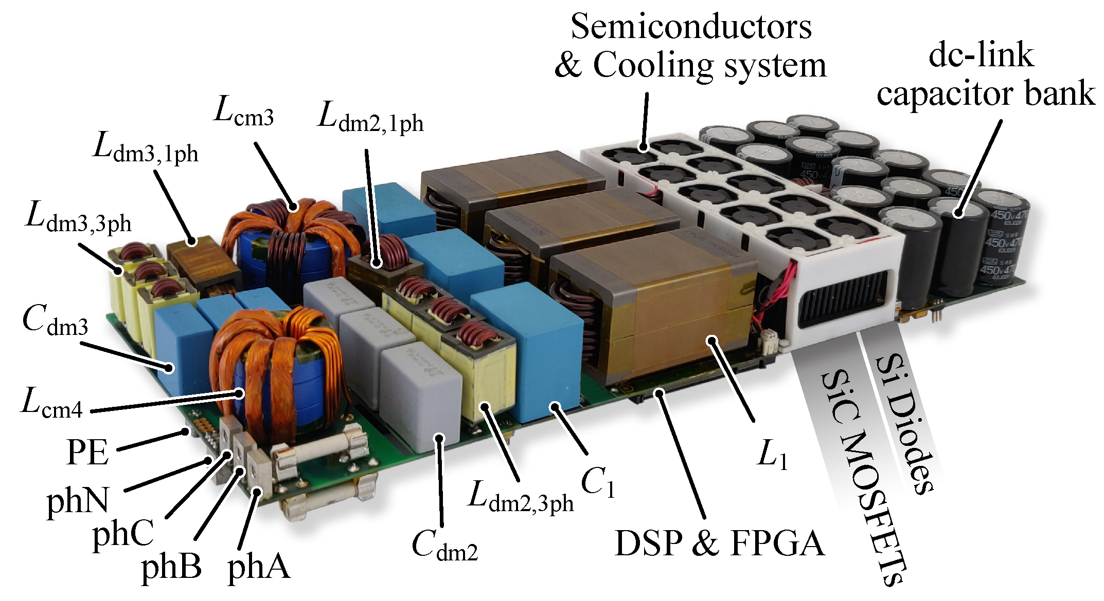
5. Experimental Results

Figure 10 depicts the realized hardware, which is designed for a dc-link voltage of 750 V and for output power levels of 22 kW and 19 kW in case of 3-phase and 1-phase operation, respectively. The boxed volume of the hardware is 3.4 dm 3 . The EMI measurements are conducted with the ESPI Test Receiver [46] and ENV216 single-phase Line Impedance Stabilization Networks (LISN) [47] (one per phase), both manufactured by Rohde & Schwarz. The measurements employ the peak detector, which, compared to the QP detector, is much faster and provides a worst-case result of the noise spectrum. The experimental setup is realized according to the guideline presented in [28]. For the measurements, a grounded metal plate has been placed below the hardware, to emulate a hardware enclosure. However, the plate has a minor impact and is only effective in case of 1-phase operation, where the measured noise decreases by ≈3 dB for frequencies greater than 20 MHz.
The maximum rms value of the phase current of the employed LISN is 16 A, which limits the power in 1-phase operation to approximately 4 kW. Therefore, in the following, the main findings of this work are verified by measuring the EMI generated by the realized hardware at a power output of 4.5 kW for both 3-phase and 1-phase operation (during the 1-phase measurements, the employed LISNs were thermally monitored, to ensure safe operation). As all parts of the power stage (e.g., SiC MOSFETs, heat sink, inductors, capacitors, and PCB tracks) are designed for the full power levels specified in Table 1 (despite the limited power level of the EMI test), the hardware comprises parasitic components and exhibits the EMI filter attenuation characteristics of a final high power system.
With regard to the HF equivalent circuits depicted in Figure 6 and Figure 7, the generated EMI noise voltages mainly depend on the voltages at the switch-nodes and, therefore, on the dc-link voltage and the modulation index [48]. This has been analyzed in the course of further circuit simulations that have been conducted for two different dc-link voltages (375 V and 750 V), same modulation indices of M = 0.867 , and same output dc currents of 29.3 A. The resulting DM and CM components are shown in Figure 11 (gray curve: V dc = 750 V ; black curve: V dc = 375 V ). Both, DM and CM characteristics increase by 6 dB if the dc-link voltage increases by a factor of two. Accordingly, it is important to test the EMI performance of the rectifier at the rated dc-link voltage of 750 V.
In theory, the EMI noise voltages are independent of the output power. However, in a practical system, different implications may disturb this property:
  • The influence of the switched currents on the switching speeds of the employed SiC MOSFETs, in particular during turn-off [49]. With increasing currents, the switching speeds increase and, with this, the EMI noise in the higher frequency ranges also increases. With regard to the setup at hand, a worst-case scenario with constant rise and fall times of 20 ns for all drain-source voltages during switching has been considered. With this, the envelope of the simulated EMI noise spectrum decays with 20 dB/decade for f s < f < 16 MHz .
  • The inductors, which are realized with powder cores, feature inductances that decrease with increasing currents. Accordingly, the efficacy of the filter decreases for higher inductor currents [50].
  • The HF current components in the commutation loops depend on the load current and the associated magnetic fields can lead to induced voltages in the EMI filter components that increase the EMI noise.
  • Increased power leads to increased temperatures of the EMI filter components. However, this effect is disregarded, as the resulting tolerances are below 5%.
The impact of the output power on the EMI noise has been analyzed in the course of further circuit simulations. The simulation considers typical values of the parasitic loop inductances ( 40 nH ± 20 % ) in the three commutations loops of the 2LB6 PFC rectifier to model their impact on the EMI noise. Reverse recovery effects have been disregarded, as these are comparably low in case of SiC MOSFETs [48]. The hardware is realized such that the EMI filter components that are closest to the mains (and, thus, most sensitive to induced voltages) are placed as far away from the switching stage as possible. With this, the implications of voltages induced by the HF magnetic fields generated by the commutation loops on the filtered EMI noise are negligible. As a result, the impact of nonlinear filter inductances on the EMI performance remains. The simulation results presented in Figure 11 consider boost inductors that feature the inductance characteristic, L 1 ( i ) , which results for the employed powder cores, cf., Table 4. This figure reveals a slight increase of the DM noise (by less than 2 dB) and a negligible change of the CM noise. Accordingly, only a minor impact of the load current on the EMI performance is expected as, e.g., also shown in Figure 9 in [51]. Overall, this section provides a proof of concept, i.e., the effective attenuation of the generated noise of the proposed topology for same output power in case of 3-phase and 1-phase operation.

5.1. 3-Phase Operation

Figure 12 shows measured waveforms of v ab and the three-phasecurrents of the converter during 3-phase rectifier operation, at an output power of 4.5 kW and for an rms line-to-neutral voltage of 230 V. The rms current per phase is 6.5 A with a Total Harmonic Distortion (THD) of 3.2%. The waveforms are recorded using the HDO6104 oscilloscope from Teledyne Lecroy. The EMI measurement result for the same operating condition is shown in Figure 13. According to this result, the converter successfully complies with the CISPR 11 Class B QP regulations. Furthermore, Figure 13 reveals that the measured EMI noise decreases with approximately 20 dB / dec for increasing frequency.
A direct comparison to the simulated results depicted in Figure 5 reveals increased EMI noise also in the lower frequency range, i.e., for frequencies close to 288 kHz. Furthermore, a steeper decrease would be expected. However, according to Figure 8, the self-parasitics of the components, couplings between components, and the interconnections on the PCB decrease the DM and CM attenuations of the EMI filter. In case of the DM characteristic, deviations are already found at frequencies close to 200 kHz, due to the already very high attenuation of 100 dB. In the course of a deeper analysis, the EMI noise envelope has been estimated based on a combination of circuit simulations and measured attenuation characteristics; the gray curve in Figure 13 presents the obtained results. For this, the unfiltered QP EMI noise spectra generated at the switch-nodes (DM and CM) have been estimated with a circuit simulation. Each spectrum is multiplied with the corresponding, i.e., DM or CM, measured filter characteristic, to obtain the DM and CM spectra at the LISNs. Finally, the absolute values of the DM and CM voltage components at the LISN have been added, which estimates the result of the least desirable superposition of the two voltage components (this simplified approach neglects the conversion of DM components into CM components and vice versa). The estimated envelope of the EMI noise confirms the measured increase of the EMI noise, which is found to be mainly related to the deviations between the ideal and the measured attenuation characteristic of the DM part of the EMI filter, that are present for frequencies as low as 200 kHz, cf. Section 4.4.

5.2. 1-Phase Operation

Figure 14 depicts the boost inductor currents of the three phases, together with the switch-node voltage of phase a, during 1-phase operation at 4.5 kW. The magnified view of ten switching periods highlights the interleaved operation of the three currents and the balanced sharing of the LF component of the grid current. The measured total input current (rms value of 18.8 A) and the phase voltage (rms value of 240 V) are shown in Figure 15. (For the experiment an ac frequency of 50 Hz, instead of 60 Hz, is considered, to allow for a direct comparison of the waveforms obtained for 3-phase and 1-phase operation). Around the zero-crossings, a LF ringing can be observed in the current, which is attributed to the transition between Continuous Conduction Mode (CCM) and Discontinuous Conduction Mode (DCM). The resulting THD of the current is 6.9%, which is a typical value for a totem pole configuration at 20% partial load operation [13,53,54] (a reduction of the THD can be achieved with the concepts proposed in [55,56]). Furthermore, new EV charger designs typically require bidirectional operation; in that case, the LF bridge-leg is actively operated, which resolves the aforementioned issue.
In Figure 16, the measured EMI noise of the 1-phase operation is shown. Due to the interleaved modulation of the three phases, only multiples of three times the switching frequency are seen, e.g., 6 f s , 9 f s . In comparison to the simulated EMI spectra depicted in Figure 5 and Figure 11, a steeper decrease of the EMI noise would be expected. In order to provide further verification, the envelope of the QP EMI noise has been estimated for 1-phase operation using the same procedure that has been applied for 3-phase operation (gray curve in Figure 16). The estimated envelope predicts similar emissions of the conducted EMI noise up to 3 MHz and reveals that the characteristic of the EMI noise at frequencies below 3 MHz is mainly defined by the characteristic of the DM attenuation of the EMI filter. Compared to the 3-phase operation, the 1-phase operation leads to an increased noise floor, which originates from the displacement currents in the parasitic capacitances between the plus and minus nodes of the dc-link and PE that are due to the dc-side voltage step at every zero-crossing of the mains current, cf. Section 2 and Figure 3. Finally, at 17.8 MHz, a noise peak can be observed that exceeds the limits by 3 dB. At these frequencies, the generated noise is typically linked to CM disturbances. However, corresponding hardware improvements, to ensure compliance in this very high frequency range, would only be reasonable for a final system with a final enclosure.

6. Conclusions

The proposed universal 3-phase/1-phase front-end ac/dc converter of a 22 kW EV charger facilitates fast charging in countries providing 3-phase 400 V/ 32 A or 1-phase 240 V/ 80 A mains connections. This is expected to enable a more economic production of EV chargers both for on-board and off-board (charging stations) applications for both geographical regions.
For a 3-phase two-level six-switch (2LB6) converter topology, this is achieved with a modified power stage that provides a return path for the current in case of 1-phase operation, through a dedicated return conductor and a diode bridge-leg, and a novel EMI filter structure that features 4-phase Common Mode (CM) chokes, which do not saturate in case of 3-phase or 1-phase operation. The proposed modifications can be directly applied to multilevel 3-phase rectifier topologies that do not require a connection to the dc-link midpoint (e.g., flying capacitor converters). The extension to a three-level T-type converter is outlined in Appendix C.
The stresses of the main power components (semiconductors, boost inductor, and dc-link capacitors) are analyzed for the 2LB6 topology for 3-phase and 1-phase operation, and based on the results, a design guideline of the power stage is presented. Furthermore, the conducted EMI noise is analyzed and the efficacies of the filter components are discussed for both operating modes, which enables the compilation of a guideline for the design of the EMI filter.
The discussed solution is validated with circuit simulations and a prototype is designed based on common practical considerations for an output power of 22 kW (3-phase operation) and 19 kW (1-phase operation). The boxed volume of the realized prototype is 3.4 dm 3 . Due to the current limitations of the employed LISNs, EMI measurements are conducted at a reduced output power of 4.5 kW, which is justified by the fact that the characteristic of the noise source is mainly defined by the dc-link voltage level and the modulation index, and not the processed current. The measurement results confirm the findings of this work, i.e., the EMI filter complies with CISPR 11 Class B QP regulations under 3-phase and 1-phase operation.
The versatility of the proposed solution comes at an increase of the converter volume from 2.7 dm 3 to 3.4 dm 3 , mostly due to the additional capacitance of the dc-link (plus 0.5 dm 3 ), but also due to the losses of the diode bridge-leg, thus, a slightly larger cooling system and the increased volume of the EMI filter. In return, the proposed solution features low complexity and the modifications are of low cost.

Author Contributions

Conceptualization, P.P., F.K., and J.W.K.; methodology, P.P.; software, P.P.; validation, P.P., D.B., and D.M.; formal analysis, P.P.; investigation, P.P.; resources, J.W.K.; data curation, P.P.; writing—original draft preparation, P.P.; writing—review and editing, P.P., F.K., and J.W.K.; supervision, J.W.K.; project administration, J.W.K. All authors have read and agreed to the published version of the manuscript.

Funding

This research received no external funding.

Data Availability Statement

The data presented in this study are available on request from the corresponding author.

Conflicts of Interest

The authors declare no conflict of interest.

Appendix A. Asymmetric Construction of the 4-Phase CM Choke: Implications on Stray Inductance

In order to assess the asymmetry of the construction of the CM choke depicted in Figure 4a, 2D Finite Element Method (FEM) simulations of both constructions are conducted using COMSOL Multiphysics software for the example of L cm 3 , i.e., 6 turns per phase on three stacked nanocrystalline cores featuring a relative permeability of μ r = 9000 ; outer and inner diameters of 48.4 mm and 23.9 mm, respectively; and a total height of 36.6 mm. Six different inductances are examined:
  • Three inductances of phase a:
    (a)
    For phase b being shorted: L σ , a | v b = 0
    (b)
    For phase c being shorted: L σ , a | v c = 0
    (c)
    For phases b and c being shorted: L σ , a | v b = v c = 0
  • Three inductances of phase b for separate and simultaneous short-circuits across phases a and c: L σ , b | v a = 0 , L σ , b | v c = 0 , and L σ , b | v a = v c = 0 .
Table A1 lists the computed results for a frequency of 192 kHz (this value refers to the EMI noise harmonic with the lowest frequency that is subject to EMI limitations in case of the investigated system) and Figure A1a,b shows the simulated magnetic field strengths. In case of complete symmetry,
L σ , a | v b = 0 = L σ , a | v c = 0 = L σ , b | v a = 0 = L σ , b | v c = 0 = 2 L σ
and
L σ , a | v b = v c = 0 = L σ , b | v a = v c = 0 = 1.5 L σ
apply. According to the simulation results listed in Table A1, (A1) and (A2) hold true for the symmetric construction of Figure 4b, whereas the asymmetric construction of Figure 4a reveals deviations of up to 30%, which is between L σ , a | v b = 0 and L σ , a | v c = 0 .
Figure A1. 2D FEM simulation of 4-phase CM chokes of the designs depicting the magnetic stray fields of two different constructions of a 4-phase CM choke obtained with 2D FEM simulations for the normalized case i a = i b = i c = i n / 3 = 1 A : (a) asymmetric construction and (b) symmetric construction shown in Figure 4a,b, respectively.
Electronics 10 02069 g0a1
The simulated results are validated with impedance measurements, using a high-precision impedance analyzer Agilent 4294A [39]. The measurement results are consistent with the simulations, with a maximum deviation of 20%, which is attributed to inaccuracies of the simplified 2D FEM simulations, due to unmodeled effects. The measured inductances of the symmetric construction agree with (A1) and (A2), and the measured inductances of the asymmetric construction are subject to a maximum deviation of 41%. In view of typical component tolerances, this deviation is considered to be of minor relevance, in particular, if dedicated DM filter inductors are connected in series that are reducing the overall asymmetry. However, the asymmetric construction is subject to an increased magnetic stray field, cf. Figure A1a. For this reason, additional shielding may be necessary (even though this was not needed in case of the hardware presented in this work).
Table A1. FEM simulated and measured stray inductances.
Constr.PhaseCondition Variable Sim. Meas.
Figure 4aashorted b L σ , a | v b = 0 3.87  μ H4.41  μ H
shorted c L σ , a | v c = 0 5.02  μ H6.20  μ H
shorted b, c L σ , a | v b = v c = 0 3.40  μ H4.03  μ H
bshorted a L σ , b | v a = 0 3.98  μ H4.43  μ H
shorted c L σ , b | v c = 0 3.98  μ H4.38  μ H
shorted a, c L σ , b | v a = v c = 0 2.70  μ H2.95  μ H
Figure 4bashorted b L σ , a | v b = 0 4.71  μ H5.86  μ H
shorted c L σ , a | v c = 0 4.71  μ H6.01  μ H
shorted b, c L σ , a | v b = v c = 0 3.53  μ H4.52  μ H
bshorted a L σ , b | v a = 0 4.71  μ H6.00  μ H
shorted c L σ , b | v c = 0 4.71  μ H5.80  μ H
shorted a, c L σ , b | v a = v c = 0 3.53  μ H4.40  μ H

Appendix B. Analysis of Power Components’ Stresses

Appendix B.1. 3-Phase Operation

In order to enable the calculation of the currents in the different power components for 3-phase operation, the duty cycle functions need to be calculated. The latter are directly related to the mains phase voltages that are applied to the ac port of the rectifier, which, in 3-phase operation, are given with
v { a , b , c } = 2 × V ac , rms sin 2 π f m t + + 0 120 + 120 ,
as shown in Figure A2a for a selected phase-to-neutral voltage, e.g., v a . The calculation of the expressions for the duty cycles is based on two assumptions: First, it is assumed that the power stage of the rectifier does not generate a LF CM component and, second, that the voltage drops due to EMI filter and boost inductor are negligible at mains frequency. The resulting duty cycle, e.g., for phase a, is calculated according to the work in [57] and
d 3 ph , a ( t ) = 0.5 + M sin ( 2 π f m t ) ,       M = 2 V ac , rms V dc ,
results, which is shown in Figure A2b (M is the modulation index). According to Table 1 and (A4), the duty cycles utilize the range between 13% and 87%.
Note that (A4) neglects the fact that the input current controller of the PFC rectifier needs to modify the duty cycle of each half-bridge in order to generate a fundamental inductor voltage drop and/or to achieve that every phase current is proportional to the corresponding phase-to-neutral voltage, e.g.,
i a ( t ) = 2 I ph , rms sin ( 2 π f m t )
in case of phase a. Thus, the presented design is limited to f s f m where this impact on the duty cycle function is negligible. Expressions (A4) and (A5) serve as the basis for the computation of the component stresses, e.g., the rms currents in the semiconductors.
Figure A2. (a) Phase-to-neutral voltage (black line) and phase current (gray line) of a selected phase, e.g., phase a, for 3-phase operation. (b) Change of duty cycle over time for three different operating modes: 3-phase operation (solid black line), 1-phase operation and V dc = 750 V (dashed line), 1-phase operation and V dc = 375 V (solid gray line).
Electronics 10 02069 g0a2

Appendix B.1.1. Semiconductors

The shown expressions for the semiconductor losses are based on the assumptions that the current ripple in the boost inductor can be neglected and that the rms currents in all phases are equal. In case of 3-phase operation, the dc-side unfolder bridge-leg is unused and only the MOSFETs generate conduction and switching losses. The total conduction losses of all six MOSFETs over a mains period can be calculated with
P M , c = 3 I ph , rms 2 R ds , on ,         R ds , on = R ds , on N M .
In (A6), R ds , on denotes the on-state resistance per switch, i.e., for N M parallel devices. Equation (A6) yields the conduction losses of the MOSFETs in case of 3-phase and 1-phase operation, as either the low-side or the high-side MOSFET of each bridge conducts the current of the connected boost inductor.
The local switching losses, i.e., the switching losses during one switching period, are calculated based on a second-order polynomial approximation [58],
e M , sw ( t ) = k A chip k sw , 0 + k sw , 1 i a ( t ) k A chip + k sw , 2 i a ( t ) k A chip 2 ,
where k A chip refers to the ratio of the chip areas of the employed device and the device for which the switching losses have been measured for; k A chip is approximated by the inverse ratio of the corresponding on-state resistances,
k A chip = R ds , on R ds , on N M .
There, R ds , on denotes the nominal on-state resistance of the device whose switching losses are known. (In the presented case, this is the C2M0025120D device (Wolfspeed/Cree). The measured device features R ds , on = 25 m Ω and employs a 3-pin TO-247 package. It is of the same generation as the device employed in this work. The switching losses shown in [59] are used in this work). The total switching losses can be approximately calculated from the average energy dissipated within a mains period, T m = f m 1 .
P M , sw = f m E M , sw ,       E M , sw = 1 T m T m 0 e M , sw ( t ) d t .
The evaluation of (A9) leads to the final expression for the switching losses,
P M , sw = 3 f s k A chip k sw , 0 + k sw , 1 I ph , avg k A chip + k sw , 2 I ph , rms k A chip 2 ,
which are calculated with the average absolute value,
I ph , avg = I ph , rms 2 2 π ,
and the rms value of the current in each phase.

Appendix B.1.2. Boost Inductor

The first step of the design of the boost inductor is the selection of a suitable core. Based on this, the number of turns, N; the wire diameter, d w ; and the losses can be calculated in a second step.
For defined values of inductance, L 1 ; peak flux density in the core, B pk ; maximum rms current density in the conductor, J rms ; and fill factor, k f , a suitable core can be found based on the area product, which refers to the minimum required value of the product of core cross section, A c , and core window area, A w [60], of a core,
( A c A w ) min = L 1 I ph , pk B pk I ph , rms k f J rms .
However, besides the above mentioned values and I ph , rms , also the peak current, I ph , pk , is needed to evaluate (A12). A respective derivation reveals
I ph , pk = f s L 1 I ph , rms 2 M 2 V dc + V dc 8 f s L 1 L 1 < L lim 3 p , 2 I ph , rms + ( 1 4 M 2 ) V dc 8 f s L 1 L 1 L lim 3 p ,
L lim 3 p = 1 f s M 2 V dc 2 I ph , rms ,
which takes into account that, due to the inductor current ripple, the peak of the total current and the peak of the LF mains current do not necessarily occur at the same time. With known values of A c and A w , the number of turns and the diameter of the conductor can be calculated,
N = L 1 I ph , pk A c B pk ,        d w = 4 π k f A w N .
Subsequently, the losses can be calculated. This calculation considers three main loss components: LF and HF conduction losses and HF core losses:
P L 1 = 3 P Cu , LF + P Cu , HF + P core .
LF copper losses
The LF copper losses of each boost inductor are calculated with
P Cu , LF = I ph , rms 2 R L 1 , dc ,        R L 1 , dc = N l avg σ k f A w N ,
which assumes that the LF rms inductor current and the input rms current of the converter are equal ( l avg is the average turn length and σ the conductivity).
HF copper losses
The calculation of the HF copper losses,
P Cu , HF = I L ph , rms , HF 2 R L 1 , ac ,
assumes that all spectral HF current components are concentrated at the switching frequency, i.e., R L 1 , ac is the ac resistance of the inductor at the switching frequency and I L ph , rms , HF is the rms value of all HF components of the inductor current. I L ph , rms , HF is calculated by averaging the square of the time-dependent local HF rms current, i L ph , rms , HF ( t ) , over one mains period. The local HF rms current refers to the HF rms current during one switching period and is calculated with the local HF peak current,
i L ph , rms , HF ( t ) = i L ph , pk , HF ( t ) 3 ,      i L ph , pk , HF ( t ) = 1 2 V dc ( 1 d ) L 1 d f s ,
which can be calculated in a straightforward manner, as the first filter stage does not feature a CM choke and because the capacitors of the first filter stage are connected to the midpoint, O. Based on (A19), an overall HF rms inductor current of
I L ph , rms , HF = 1 2 3 V dc f s L 1 0.0625 0.25 M 2 + 0.375 M 4
results.
The ac resistance is calculated according to the work in [61],
R L 1 , ac = 2 F r + H w , norm 2 G r R L 1 , dc ,
where F r and G r refer to the scaling factors due to skin and proximity effects; (The presented factors correspond to values compatible with the peak value of the current. For rms currents, an additional factor of 2 is needed). H w , norm denotes the magnetic field that leads to the proximity effect and is normalized with respect to the inductor current. For d w 32 1 3 δ [61] ( δ is the skin depth),
F r = d w 8 δ ,      G r = π 2 d w 3 4 δ ,      δ = 1 μ r , Cu μ 0 f s σ π
apply, which, for the considered solid copper wire, is fulfilled at f s = 48 kHz ( δ = 0.35 mm ). The value of H w , norm is calculated under the assumption of a distributed air gap on the outer and the inner core limbs (approximation for powder core). With this,
H w , norm = N 2 3 h w
results.
HF magnetic core losses
The core losses are calculated based on the assumption of a sinusoidal (instead of triangular) shape of the magnetic flux density with same peak value, B pk . Accordingly, the local core losses can be calculated with the Steinmetz Equation,
p core ( t ) = V c k SE f s α B pk ( t ) β ,        B pk ( t ) = L 1 i L ph , pk , HF ( t ) N A c ,
which is slightly overestimating the core losses that result for triangular currents [62,63]. Due to the raise of the flux density to the power of β , the average core losses are calculated by means of numerical integration,
P core = 2 T m 0 T m 2 p core ( t ) d t .

Appendix B.2. 1-Phase Operation

Similar to 3-phase operation, the function of the duty cycle needs to be determined before the currents in the different power components can be calculated. According to Figure 3, the mains voltage
v ac = 2 × 240 V sin ( 2 π f m t ) ,
is equal to the local average of the voltage between each switch-node (Figure 3A–C) and either the minus terminal of the dc-link, m, if D 2 conducts ( i ac > 0 ) or the plus terminal, p, if D 1 conducts ( i ac < 0 ). The resulting duty cycle for 1-phase operation is equal to
d 1 ph ( t ) =     M sin ( 2 π f m t ) , 2 π f m t [ 0 , π ) , 1 + M sin ( 2 π f m t ) , 2 π f m t [ π , 2 π ) .

Appendix B.2.1. Semiconductors and Boost Inductor

The calculation of the MOSFETs’ conduction and switching losses and the losses in the boost inductor is identical to Appendix B.1, however, different expressions apply to I ph , pk and I L ph , rms , HF ,
I ph , pk = 2 2 I ph , rms f s L 1 + M V dc 2 8 f s L 1 M 2 V dc L 1 < L lim 1 p , 2 I ph , rms + ( M M 2 ) V dc 2 f s L 1 L 1 L lim 1 p ,
L lim 1 p = 1 f s ( 2 M 2 M ) V dc 2 2 I ph , rms .
I L ph , rms , HF = 1 12 2 π V dc M f s L 1 12 π + M 64 + 9 M π ,
which are derived for the duty cycle function d 1 ph ( t ) , instead of d 3 ph ( t ) . In addition, the diode bridge-leg generates conduction losses, i.e.,
P D , c = ( 3 I ph , rms ) 2 r d + 3 I ph , avg V f ,
where V f denotes the current independent forward voltage drop of each diode and r d refers to the total differential resistance of N D diodes that are operated in parallel,
r d = r d N D .

Appendix B.2.2. Electrolytic Capacitors of the Dc-Link

The computation of the losses in the electrolytic dc-link capacitors only takes the LF component of the capacitor current into consideration, as ceramic capacitors are located close to the power semiconductors and effectively keep the HF current components away from the electrolytic capacitors. Commonly available electrolytic capacitors cannot provide operating voltages of 750 V. Accordingly, the dc-link employs N C parallel branches of electrolytic capacitors where each branch contains two capacitors that are connected in series. Furthermore, the calculation of the capacitor losses is based on the assumption that each capacitor has the same Equivalent Series Resistance, ESR C . With this, the losses of all electrolytic capacitors are
P C dc = I C dc , rms 2 2 ESR C N C ,        I C dc , rms = 1 2 P nom V dc .

Appendix B.3. 1-Phase Operation at Half Dc-Link Voltage

In case of 1-phase operation of the PFC rectifier shown in Figure 2, the dc-link voltage can be reduced, which expectedly leads to lower core losses in the boost inductors and lower switching losses. The reduction of V dc is possible due to the diode bridge-leg that acts as PFC unfolder circuit, such that the full dc-link voltage can be utilized to follow the mains voltage during half a mains period [64] (in comparison, the discussed 3-phase PFC rectifier can only utilize half of V dc to follow the mains voltage during half a mains period, as the dc-link voltage midpoint serves as virtual reference point for the ac voltage formation). However, the reduction of the dc-link voltage from V dc = 750 V to, e.g., half of this value, imposes the same voltage change to the input of a directly series connected power converter. Figure A3 depicts a solution that prevents supplied converters from being subject to a wide input voltage range. The additional relay circuitry connects the two capacitor banks of the dc-link and two isolated dc/dc converters either in series (3-phase operation) or in parallel (1-phase operation). With this, the same input voltages are applied to the dc/dc converters and the same LF rms currents are achieved in the two dc-link capacitors, C dc , in case of full and half dc-link voltage, V dc = 750 V and V dc = 375 V , respectively.
The losses of the main power components for 1-phase operation at half dc-link voltage can be calculated with the equations of Appendix B.2. Table A2 lists the results for 1-phase operation at half and full dc-link voltage, which reveal a substantial reduction of the switching losses and the losses in the boost inductor (due to reduced HF conduction and core losses). This leads to total losses of 226 W, i.e., less than for 3-phase operation, where total losses of 294 W result, cf. Section 3.2.
Table A2. Losses in 1-phase operation at half and full dc-link voltage.
V dc P M , c P M , sw P D , c P L 1 , Cu , LF P L 1 , Cu , HF P L 1 , core P C dc
375 V66 W38 W72 W5.6 W0.6 W5.3 W15 W
750 V66 W101 W72 W5.6 W2.9 W22.1 W15 W
Figure A3. Proposed extension of a T-type rectifier, shown for 1-phase operation with V dc = 375 V . In case of 3-phase operation, the relay contact S 1 is closed and S 2 { i , ii } change their positions such that the two dc-link capacitors are connected in series and withstand the full dc-link voltage of 750 V. © 2019 IEEE. Adapted from Ref. [12].
Electronics 10 02069 g0a3

Appendix C. Extension to Three-Level Converters with Inherent Utilization of the Dc Midpoint

A direct extension of converters with inherent utilization of the dc midpoint (e.g., T-type converter) by a diode bridge-leg according to Figure 2 would lead to very high LF rms currents in the dc-link capacitors in case of three-level operation and 1-phase ac input, because each capacitor of the split dc-link, C dc , would only be charged every second mains half period, i.e., in an alternating manner [65]. A practical solution to mitigate this undesirable property is to change the operating mode of the converter depending on the type of mains supply:
  • Three-level operation for 3-phase mains connection (middle leg enabled, V dc = 750 V ).
  • Two-level operation for 1-phase ac input (middle leg disabled, V dc = 375 V ).
In this regard, the dc-link voltage is reduced to 375 V during 1-phase operation in order to achieve similar cores losses (and ripple currents) in the PFC inductors and similar switching losses in both operating modes listed above. The circuit shown in Figure A3, which realizes the modifications listed below, can be used to achieve constant input voltages for series-connected dc/dc converters:
  • A relay circuit for series/parallel reconfiguration of the dc-link capacitors and the subsequent dc/dc converters is provided.
  • The middle power switches of the T-type converter are connected to the switch-node of the diode rectifier, O’, as the electrical potential of O’ is always defined (the node O is floating during 1-phase operation).
With this circuit, the input voltages of the dc/dc converters are equal to 375 V, independent of whether 3-phase or 1-phase operation applies. Furthermore, the LF rms current in each capacitor of the dc-link in 1-phase operation is equal to the one of the 2LB6 converter operating in 1-phase mode (cf. Figure 2).

References

  1. Plugs, Socket-Outlets, Vehicle Connectors and Vehicle Inlets—Conductive Charging of Electric Vehicles. IEC 62196.
  2. SAE Surface Vehicle Recommended Practice J1772, SAE Electric Vehicle Conductive Charge Coupler. SAE J1772.
  3. Byczek, R. EVSE Testing and Global Certifications—What Manufacturers Need to Know. Available online: https://www.intertek.com/blog/2020-10-02-evse/ (accessed on 17 August 2021).
  4. PFM-Isolated & Regulated Converter with PFC for AC–DC Systems. Available online: http://www.vicorpower.com/ac-dc/converters/isolated-ac-dc-converter-pfc (accessed on 22 December 2020).
  5. Schmenger, J.; Endres, S.; Zeltner, S.; März, M. A 22 kW on-board charger for automotive applications based on a modular design. In Proceedings of the IEEE Conference on Energy Conversion (CENCON), Johor Bahru, Malaysia, 13–14 October 2014. [Google Scholar] [CrossRef]
  6. Lu, J.; Bai, K.; Taylor, A.R.; Liu, G.; Brown, A.; Johnson, P.M.; McAmmond, M. A modular-designed three-phase high-efficiency high-power-density EV battery charger using dual/triple-phase-shift control. IEEE Trans. Power Electron. 2018, 33, 8091–8100. [Google Scholar] [CrossRef]
  7. Yoo, K.; Kim, K.; Lee, J. Single- and three-phase PHEV onboard battery charger using small link capacitor. IEEE Trans. Ind. Electron. 2013, 60, 3136–3144. [Google Scholar] [CrossRef]
  8. Wang, X.; Jiang, C.; Lei, B.; Teng, H.; Bai, H.K.; Kirtley, J.L. Power-loss analysis and efficiency maximization of a silicon-carbide MOSFET-based three-phase 10-kW bidirectional EV charger using variable-DC-bus control. IEEE J. Emerg. Sel. Top. Power Electron. 2016, 4, 880–892. [Google Scholar] [CrossRef]
  9. Zhao, H.; Shen, Y.; Ying, W.; Ghosh, S.S.; Ahmed, M.R.; Long, T. A single- and three-phase grid compatible converter for electric vehicle on-board chargers. IEEE Trans. Power Electron. 2020, 35, 7545–7562. [Google Scholar] [CrossRef]
  10. BRUSA Elektronik AG. NLG664-On Board Fast Charger. NLG664 Datasheet. 2018. Available online: https://www.brusa.biz/wp-content/uploads/2021/03/BRUSA_DB_EN_NLG664.pdf (accessed on 26 August 2021).
  11. Stengert, K. On-board 22 kW fast charger ‘NLG6’. In Proceedings of the World Electric Vehicle Symposium and Exhibition (EVS27), Barcelona, Spain, 17–20 November 2013. [Google Scholar]
  12. Papamanolis, P.; Krismer, F.; Kolar, J.W. 22 kW EV battery charger allowing full power delivery in 3-phase as well as 1-phase operation. In Proceedings of the IEEE International Conference on Power Electronics (ICPE-ECCE Asia), Busan, Korea, 27–31 May 2019. [Google Scholar] [CrossRef]
  13. Gong, X.; Wang, G.; Bhardwaj, M. 6.6 kW three-phase interleaved totem pole PFC design with 98.9% peak efficiency for HEV/EV onboard charger. In Proceedings of the Applied Power Electronics Conference and Exposition (APEC), Anaheim, CA, USA, 17–21 March 2019. [Google Scholar] [CrossRef]
  14. Kolar, J.W.; Drofenik, U.; Miniböck, J.; Ertl, H. A new concept for minimizing high-frequency common-mode EMI of three-phase PWM rectifier systems keeping high utilization of the output voltage. In Proceedings of the IEEE Applied Power Electronics Conference and Exposition sition (APEC), New Orleans, LA, USA, 6–10 February 2000. [Google Scholar] [CrossRef]
  15. Dong, D.; Zhang, X.; Luo, F.; Boroyevich, D.; Mattavelli, P. Common-mode EMI noise reduction for grid-interface converter in low-voltage DC distribution system. In Proceedings of the IEEE Applied Power Electronics Conference and Exposition (APEC), Orlando, FL, USA, 5–9 February 2012. [Google Scholar] [CrossRef]
  16. Hartmann, M.; Ertl, H.; Kolar, J.W. EMI filter design for a 1 MHz, 10 kW three-phase/level PWM rectifier. IEEE Trans. Power Electron. 2011, 26, 1192–1204. [Google Scholar] [CrossRef]
  17. Shi, K.; Shoyama, M.; Tomioka, S. Common mode noise reduction in totem-pole bridgeless PFC converter. In Proceedings of the IEEE International Power Electronics and Application Conference and Exposition (PEAC), Shanghai, China, 5–8 November 2014. [Google Scholar] [CrossRef]
  18. Zhang, B.; Lin, Q.; Imaoka, J.; Shoyama, M.; Tomioka, S.; Takegami, E. Conducted noise prediction for zero-crossing issue in totem-pole bridgeless PFC converter. In Proceedings of the IEEE International Telecommunications Energy Conference (INTELEC), Broadbeach, Australia, 22–26 October 2017. [Google Scholar] [CrossRef]
  19. Qu, S.; Chen, D. Mixed-mode EMI noise and its implications to filter design in offline switching power supplies. IEEE Trans. Power Electron. 2002, 17, 502–507. [Google Scholar] [CrossRef]
  20. Jin, M.; Weiming, M. A new technique for modeling and analysis of mixed-mode conducted EMI noise. IEEE Trans. Power Electron. 2004, 19, 1679–1687. [Google Scholar] [CrossRef]
  21. Kolar, J.W.; Krismer, F.; Lobsiger, Y.; Muhlethaler, J.; Nussbaumer, T.; Minibock, J. Extreme efficiency power electronics. In Proceedings of the IEEE International Conference on Integrated Power Electronics Systems (CIPS), Nuremberg, Germany, 6–8 March 2012. [Google Scholar]
  22. Boillat, D.O.; Krismer, F.; Kolar, J.W. Optimization and comparative evaluation of multiloop control schemes for controllable ac sources with two-stage LC output filters. IEEE Trans. Power Electron. 2016, 31, 7353–7368. [Google Scholar] [CrossRef]
  23. Krismer, F.; Böhler, J.; Kolar, J.W.; Pammer, G. New series-resonant solid-state DC transformer providing three self-stabilized isolated medium-voltage input ports. In Proceedings of the International Conference on Power Electronics (ICPE-ECCE Asia), Busan, Korea, 27–30 May 2019. [Google Scholar]
  24. Papamanolis, P.; Guillod, T.; Krismer, F.; Kolar, J.W. Minimum loss operation and optimal design of high-frequency inductors for defined core and litz wire. IEEE Open J. Power Electron. 2020, 1, 469–487. [Google Scholar] [CrossRef]
  25. Kanyakam, S.; Bureerat, S. Multiobjective optimization of a pin-fin heatsink using evolutionary algorithms. J. Electron. Packag. 2012, 134, 021008. [Google Scholar] [CrossRef]
  26. Thermal Resistance Calculator—Round Pin Heat Sink. Available online: https://myheatsinks.com/calculate/thermal-resistance-round-pin/ (accessed on 8 May 2021).
  27. Infineon Technologies AG. Comprehensive Solutions for Fast EV Charging Design 2019. Available online: https://infineoncommunity.com/register_for_ev_charging_whitepaper_presentation_ID1048?ic=00d1003 (accessed on 20 June 2021).
  28. Heldwein, M.L. EMC Filtering of Three-Phase PWM Converters. Ph.D. Thesis, ETH Zurich, Zurich, Switzerland, 2008. [Google Scholar]
  29. Xie, Y.; Chen, C.; Huang, Z.; Liu, T.; Kang, Y.; Luo, F. High frequency conducted EMI investigation on packaging and modulation for a SiC-based high frequency converter. IEEE J. Emerg. Sel. Top. Power Electron. 2019, 7, 1789–1804. [Google Scholar] [CrossRef]
  30. Zhang, B.; Wang, S. A survey of EMI research in power electronics systems with wide-bandgap semiconductor devices. IEEE J. Emerg. Sel. Top. Power Electron. 2020, 8, 626–643. [Google Scholar] [CrossRef]
  31. Ye, H.; Yang, Z.; Dai, J.; Yan, C.; Xin, X.; Ying, J. Common mode noise modeling and analysis of dual boost PFC circuit. In Proceedings of the IEEE International Telecommunications Energy Conference (INTELEC), Chicago, IL, USA, 19–23 September 2004. [Google Scholar] [CrossRef]
  32. Wang, S.; Kong, P.; Lee, F.C. Common Mode Noise Reduction for Boost Converters Using General Balance Technique. IEEE Trans. Power Electron. 2007, 22, 1410–1416. [Google Scholar] [CrossRef]
  33. Boillat, D.O.; Krismer, F.; Kolar, J.W. EMI filter volume minimization of a three-phase, three-level T-type PWM converter system. IEEE Trans. Power Electron. 2017, 32, 2473–2480. [Google Scholar] [CrossRef]
  34. Heldwein, M.L.; Nussbaumer, T.; Kolar, J.W. Differential mode EMC input filter design for three-phase ac-dc-ac sparse matrix PWM converters. In Proceedings of the IEEE Power Electronics Specialists Conference (PESC), Aachen, Germany, 20–25 June 2004. [Google Scholar]
  35. Silva, M.; Hensgens, N.; Oliver, J.; Alou, P.; García, Ó.; Cobos, J.A. New considerations in the input filter design of a three-phase buck-type PWM rectifier for aircraft applications. In Proceedings of the IEEE Energy Conversion Congress and Exposition (ECCE USA), Phoenix, AZ, USA, 17–22 September 2011. [Google Scholar]
  36. West, R. Common Mode Inductors for EMI Filters Require Careful Attention to core Material Selection. PCIM Mag. 1995. Available online: https://elnamagnetics.com/wp-content/uploads/library/Magnetics-Documents/Common_Mode_Inductors_for_EMI_Filters_Require_Careful_Attention_to_Core_Material_Selection.pdf (accessed on 15 May 2021).
  37. Wang, S.; Lee, F.C.; Chen, D.Y.; Odendaal, W.G. Effects of parasitic parameters on EMI filter performance. IEEE Trans. Power Electron. 2004, 19, 869–877. [Google Scholar] [CrossRef]
  38. Rossetto, L.; Buso, S.; Spiazzi, G. Conducted EMI issues in a 600-W single-phase boost PFC design. IEEE Trans. Ind. Appl. 2000, 36, 578–585. [Google Scholar] [CrossRef] [Green Version]
  39. Agilent 4294A—Precision Impedance Analyzer 40 Hz to 110 MHz. Available online: http://literature.cdn.keysight.com/litweb/pdf/5968-3808E.pdf (accessed on 16 October 2020).
  40. Wang, R.; Boroyevich, D.; Blanchette, H.F.; Mattavelli, P. High power density EMI filter design with consideration of self-parasitic. In Proceedings of the IEEE Applied Power Electronics Conference and Exposition (APEC), Orlando, FL, USA, 5–9 February 2012. [Google Scholar] [CrossRef]
  41. Vector Network Analyzer. Available online: https://www.picotest.com/images/download/Bode-100_Product_Brochure_V7-2002.pdf (accessed on 22 December 2020).
  42. Wang, R.; Fortin Blanchette, H.; Mu, M.; Boroyevich, D.; Mattavelli, P. Influence of high-frequency near-field coupling between magnetic components on EMI filter design. In Proceedings of the IEEE Applied Power Electronics Conference and Exposition (APEC), Long Beach, CA, USA, 17–21 March 2013. [Google Scholar] [CrossRef]
  43. Wang, S.; Lee, F.; Odendaal, W. Improving the performance of boost PFC EMI filters. In Proceedings of the IEEE Applied Power Electronics Conference and Exposition (APEC), Miami Beach, FL, USA, 9–13 February 2003. [Google Scholar] [CrossRef]
  44. Bishnoi, H.; Mattavelli, P.; Burgos, R.; Boroyevich, D. EMI behavioral models of DC-fed three-phase motor drive systems. IEEE Trans. Power Electron. 2014, 29, 4633–4645. [Google Scholar] [CrossRef]
  45. Sun, B.; Burgos, R.; Boroyevich, D. Common-mode EMI unterminated behavioral model of wide-bandgap-based power converters operating at high switching frequency. IEEE J. Emerg. Sel. Top. Power Electron. 2019, 7, 2561–2570. [Google Scholar] [CrossRef]
  46. R & S ESPI Test Receiver. Available online: https://www.rohde-schwarz.com/us/product/espi-productstartpage_63493-8645.html?change_c=true (accessed on 22 December 2020).
  47. R & S ENV216 Two-Line V-Network. Available online: https://www.rohde-schwarz.com/us/product/env216-productstartpage_63493-9775.html?change_c=true (accessed on 22 December 2020).
  48. Laird, I.; Yuan, X.; Scoltock, J.; Forsyth, A.J. A design optimization tool for maximizing the power density of 3-phase DC–AC converters using silicon carbide (SiC) devices. IEEE Trans. Power Electron. 2018, 33, 2913–2932. [Google Scholar] [CrossRef] [Green Version]
  49. Charalambous, A.; Yuan, X.; McNeill, N. High-frequency EMI attenuation at source with the auxiliary commutated pole inverter. IEEE Trans. Power Electron. 2018, 33, 5660–5676. [Google Scholar] [CrossRef] [Green Version]
  50. Liu, Y.; See, K.Y.; Tseng, K.J. Conducted EMI prediction of the PFC converter including nonlinear behavior of boost inductor. IEEE Trans. Electromagn. Compat. 2013, 55, 1107–1114. [Google Scholar] [CrossRef]
  51. Ibuchi, T.; Kamikomaki, R.; Funaki, T. Experimental evaluation on time variation of conducted noise spectrum for a PFC converter. In Proceedings of the International Symposium on Electromagnetic Compatibility, Tokyo, Japan, 12–16 May 2014. [Google Scholar] [CrossRef]
  52. HDO6104A. Available online: https://teledynelecroy.com/oscilloscope/hdo6000a-high-definition-oscilloscopes/hdo6104a (accessed on 22 December 2020).
  53. Zhu, K.; O’Grady, M.; Dodge, J.; Bendel, J.; Hostetler, J. 1.5 kW single phase CCM totem-pole PFC using 650V SiC cascodes. In Proceedings of the IEEE Workshop on Wide Bandgap Power Devices and Applications (WiPDA), Fayetteville, AR, USA, 7–9 November 2016. [Google Scholar] [CrossRef]
  54. Sun, J.; Strain, N.N.; Costinett, D.J.; Tolbert, L.M. Analysis of a GaN-based CRM totem-pole PFC converter considering current sensing delay. In Proceedings of the IEEE Energy Conversion Congress and Exposition (ECCE USA), Baltimore, MD, USA, 29 September–3 October 2019. [Google Scholar] [CrossRef]
  55. De Gusseme, K.; de Sype, D.; Van den Bossche, A.; Melkebeek, J. Sample correction for digitally controlled boost PFC converters operating in both CCM and DCM. In Proceedings of the IEEE Applied Power Electronics Conference and Exposition (APEC), Miami Beach, FL, USA, 9–13 February 2003. [Google Scholar] [CrossRef] [Green Version]
  56. De Gusseme, K.; Van de Sype, D.; Van den Bossche, A.; Melkebeek, J. Digital control of boost PFC converters operating in both continuous and discontinuous conduction mode. In Proceedings of the IEEE Power Electronics Specialists Conference (PESC), Aachen, Germany, 20–25 June 2004. [Google Scholar] [CrossRef]
  57. Mohan, N.; Undeland, T.M.; Robbins, W.P. Power Electronics: Converters, Applications, and Design, 3rd ed.; John Wiley & Sons Inc.: Hoboken, NJ, USA, 2002. [Google Scholar]
  58. Deboy, G.; Haeberlen, O.; Treu, M. Perspective of loss mechanisms for silicon and wide band-gap power devices. IEEE CPSS Trans. Power Electron. Appl. 2017, 2, 89–100. [Google Scholar] [CrossRef]
  59. Krismer, F.; Hatipoglu, E.; Kolar, J.W. Novel isolated bidirectional integrated dual three-phase active bridge (D3AB) PFC rectifier. In Proceedings of the IEEE International Power Electronics Conference (IPEC-ECCE Asia), Niigata, Japan, 20–24 May 2018. [Google Scholar] [CrossRef]
  60. McLyman, C. Transformer and Inductor Design Handbook; CRC Press: Boca Raton, FL, USA, 2017. [Google Scholar] [CrossRef]
  61. Leibl, M. Three-Phase PFC Rectifier and High-Voltage Generator for X-ray Systems. Ph.D. Thesis, ETH Zurich, Zurich, Switzerland, 2017. [Google Scholar]
  62. Albach, M.; Durbaum, T.; Brockmeyer, A. Calculating core losses in transformers for arbitrary magnetizing currents—A comparison of different approaches. In Proceedings of the IEEE Power Electronics Specialists Conference (PESC), Baveno, Italy, 23–27 June 1996. [Google Scholar] [CrossRef]
  63. Leicht, J.; Moses, A.; Zurek, S. Hysteresis loss component under non-sinusoidal flux waveforms. J. Magn. Magn. Mater. 2008, 320, e608–e610. [Google Scholar] [CrossRef]
  64. Azurza, J.A.; Zulauf, G.; Papamanolis, P.; Hobi, S.; Mirić, S.; Kolar, J.W. Three levels are not enough: Scaling laws for multilevel converters in AC/DC applications. IEEE Trans. Power Electron. 2021, 36, 3967–3986. [Google Scholar] [CrossRef]
  65. Chen, J.; Wang, C. Topology and voltage-balance control of a single-phase double T-type seven-level inverter. IEEE J. Emerg. Sel. Top. Power Electron. 2021, 9, 1075–1087. [Google Scholar] [CrossRef]
Figure 1. Block diagrams of conventional boost-type 3-phase ac/dc converters for different operating conditions: (a) operation from 3-phase mains and (b) operation from 1-phase mains [9,10,11].
Electronics 10 02069 g001
Figure 2. Proposed two-level six-switch (2LB6) 3-phase boost-type PFC ac/dc converter with three-stage EMI filter. Compared to a conventional 2LB6 rectifier topology, the additional components, highlighted with red color, allow full/rated power delivery also for 1-phase operation; otherwise, the 1-phase rating would be limited to 1/3 of the rated 3-phase power (cf. Figure 1b). The relay contact is closed in 3-phase operation and open in 1-phase operation, cf. Section 2. © 2019 IEEE. Adapted from Ref. [12].
Electronics 10 02069 g002
Figure 3. Illustration of the voltage loops (I and II) used to estimate v O , PE under 1-phase operation. Both loops encompass PE, O’, O, and the currently conducting rectifier diode. The voltage drop caused by the EMI filter is neglected.
Electronics 10 02069 g003
Figure 4. Two different constructions of a 4-phase CM choke with toroidal core and 6 turns per phase: (a) the winding of the 4th phase is not split apart and (b) the winding of the 4th phase is split into three parts that are connected in series. © 2019 IEEE. Adapted from Ref. [12].
Electronics 10 02069 g004
Figure 5. Simulation results for the proposed 22 kW EV charger and/or ac/dc converter specified in Table 1, with the EMI filter of Figure 2 and the filter component values of Table 7. Main waveforms and conducted EMI: (a,c) for 3-phase and (b,d) for 1-phase operation. © 2019 IEEE. Adapted from Ref. [12].
Electronics 10 02069 g005
Figure 6. (a) HF equivalent circuit of the 2LB6 converter shown in Figure 2, for 3-phase operation; (b) CM equivalent circuit; (c,d) effective CM equivalent circuit, derived in the style of [31,32]. © 2019 IEEE. Adapted from Ref. [12].
Electronics 10 02069 g006
Figure 7. (a) HF equivalent circuit of the 2LB6 converter shown in Figure 2, for 1-phase operation; the conduction paths of the HF current harmonics at ( 3 k + 1 ) f s and ( 3 k + 2 ) f s , k N 0 , are highlighted; (b) DM 1-phase equivalent circuit considering the HF current harmonics at ( 3 k + 3 ) f s , k N 0 ; (ce) CM equivalent circuit considering C par , sw > 0 . © 2019 IEEE. Adapted from Ref. [12].
Electronics 10 02069 g007
Figure 8. Comparison of (a) DM and (b) CM filter transfer functions: (i) calculated for ideal components (dashed lines), (ii) calculated based on individually measured impedance characteristics for each filter component (solid black lines), and (iii) measured directly on the PCB using the Bode100 network analyzer from OmicronLab (solid red lines).
Electronics 10 02069 g008
Figure 9. Equivalent filter circuits for the measurements of the (a) DM and (b) CM transfer functions shown in Figure 8a,b.
Electronics 10 02069 g009
Figure 10. Realized EV charger mains interface, designed for a rated power of 22 kW, that allows for rated/full power delivery in both 3-phase and 1-phase operation. The boxed volume of the system is 3.4 dm 3 . The realized hardware has been tested with an output power of 4.5 kW.
Electronics 10 02069 g010
Figure 11. (a) Simulated DM and (b) CM EMI noise components obtained for different operating conditions. The black curve represents rated operation, the red curve refers to the condition during the conducted EMI measurements, and the gray curve represents operation with half of the rated dc-link voltage (which, for same converter currents, implies half of the rated output power).
Electronics 10 02069 g011
Figure 12. Ac waveforms of the three input currents, i a , i b , i c , and line-to-line voltage, v ab , in 3-phase operation at 4.5 kW/230 V/50 Hz. The measurement is acquired using the HDO6104 oscilloscope from Teledyne Lecroy [52].
Electronics 10 02069 g012
Figure 13. EMI measurement for 3-phase operation at 4.5 kW/230 V/50 Hz (cf. Figure 12). The measured noise reveals compliance with the CISPR 11 Class B QP limits. For the measurement a Peak detector is employed that, potentially, overestimates the measured noise compared to a QP detector, nevertheless, is faster. The employed equipment is three ENV216 single-phase Line Impedance Stabilization Networks (LISN) from Rohde & Schwarz (one per phase) and an ESPI Test Receiver from the same manufacturer.
Electronics 10 02069 g013
Figure 14. Waveforms of the boost inductor currents, i L a , i L b , i L c , and the switch-node voltage of phase a, v AO , of the three phases in 1-phase operation at 4.5 kW/240 V/50 Hz. The measurement is acquired using the HDO6104 oscilloscope from Teledyne Lecroy [52]. The top part of the figure depicts the envelopes of i L a , i L b , i L c , and v AO . The marked (brightened) narrow time interval in the middle of the top part refers to the magnified presentation of the waveforms given in the bottom part of this figure.
Electronics 10 02069 g014
Figure 15. Waveforms of input current, i ac , and the grid voltage, v ac , in 1-phase operation at 4.5 kW/240 V/50 Hz. The measurement is acquired using the HDO6104 oscilloscope from Teledyne Lecroy [52].
Electronics 10 02069 g015
Figure 16. EMI measurement for 1-phase operation at 4.5 kW/240 V/50 Hz (cf. Figure 15). The measured noise reveals compliance with the CISPR 11 Class B QP limits. For the measurement a Peak detector is employed that, potentially, overestimates the measured noise compared to a QP detector, nevertheless, is faster. The employed equipment is three ENV216 single-phase Line Impedance Stabilization Networks (LISN) from Rohde & Schwarz (one per phase) and an ESPI Test Receiver from the same manufacturer.
Electronics 10 02069 g016
Table 1. Specifications of the EV charger. 2019 IEEE. Adapted from Ref. [12].
ParameterDescription3-Phase1-Phase
P nom Nominal power22 kW19.2 kW
V ac , rms Grid input voltage (rms) 3 ×  230 V240 V
I ac , rms Grid input current (rms)32 A80 A
I ph , rms Phase current (rms)32 A26.67 A
f m Grid frequency50 Hz60 Hz
V dc Output voltage750 V750 V
f s Switching frequency48 kHz
Table 2. Components’ current stresses for 3-phase and 1-phase operation.
ParameterDescription3-Phase1-Phase
I ph , rms rms value of i ph ( t ) 32 A27 A
I ph , avg average value of | i ph ( t ) | 29 A24 A
I ph , pk peak value of | i ph ( t ) | 50 A57 A
I L ph , rms , HF rms value of the HF components of i L ph ( t ) 5.1 A6.0 A
I C dc , rms rms value of the LF current in the dc-link cap. 0 18 A
Table 3. Selected power components.
ParameterValue
Power MOSFETs (per switch) two parallel C2M0040120D devices (Wolfspeed/Cree)
Power diodes (per diode) three parallel VS-80APF10 devices (Vishay)
Boost inductorssummarized in Table 4
Dc-link capacitors 14 ESMR451VSN471MR40S devices ( 2 × 7 parallel) (450 V, 470 μ F , ESR C 160 m at 60 C, I C , rms , max = 2.66 A rated at 120 Hz ; UnitedChemi Con )
Table 4. Design parameters of the boost inductor L 1 .
ParameterValue
Magnetic coreKoolMu ( μ r = 60 ) 5 × E 40/20
Number of turns (N)15
Initial inductance ( L ( I L = 0 ) )170  μ H
Inductance at peak current ( L ( I L = 57 A ) )80  μ H
Core volume ( V c ) 90,000 mm 3
Core cross section ( A c ) 915 mm 2
Area of the core window ( A w ) 258.3 mm 2
Height of the core window ( h w )29.8 mm
Average turn length ( l avg )214.3 mm
Copper fill factor ( k f )55%
Conductor diameter ( d w )3.0 mm
Steinmetz par. ( k SE , α , β ) 5.21 , 1.36 , 2.78
Table 5. Estimated losses of the main power components for 3-phase and 1-phase operation.
ParameterDescription3-Phase1-Phase
P M , c MOSFET cond. losses94.7 W66.3 W
P M , sw MOSFET switch. losses119.6 W101.3 W
P D , c Diode cond. losses-71.7 W
P L 1 , Cu , LF Boost induct. LF copper losses8.0 W5.6 W
P L 1 , Cu , HF Boost induct. HF copper losses2.1 W2.9 W
P L 1 , core Boost induct. core losses16.5 W22.1 W
P C dc dc-link cap. losses-15 W
Table 6. EMI generated noise and filter attenuation.
SourceOperationCISPR
Freq.
(kHz)
Max
Noise
(dB μ V)
Filter
Att.
(dB)
Class B
Limit
(dB μ V)
v dm , { A , B , C } 3-phase19216211663.9
v cm , par 3-phase19211871
v dm , ( 3 k + 3 ) 1-phase288162.315060.3
v cm , par 1-phase28812673
Obtained from numerical calculations and (4). Calculated for the component values listed in Table 7.
Table 7. EV charger: Values of the EMI Filter Components. 2019 IEEE. Adapted from Ref. [12].
ParameterDescriptionValue
L 1 Inductance of 1st filter stage 150 μ H
C 1 Capacitance of 1st filter stage 10 μ F
L dm 2 DM filter ind., 2nd filter stage 3.5 μ H
C dm 2 DM filter cap., 2nd filter stage 3.3 μ F
L dm 3 DM filter ind., 3rd filter stage 5.5 μ H
C dm 3 DM filter cap., 3rd filter stage 2.2 μ F
L cm 3 CM filter ind., 3rd filter stage 1.6 mH ( 1.2 mH )
C cm 3 CM filter cap., 3rd filter stage 20 nF
L cm 4 CM filter ind., 4th filter stage 1.0 mH ( 0.75 mH )
C cm 0 CM filter cap., dc-side 15 nF
C dc Capacitor of split dc-link 3.3 mF
* Corresponds to the initially defined theoretical value and to the value considered for the calculated/simulated attenuations; ** This results from the series connection of L dm 3 = 2.5 μ H with the stray inductance of L cm 3 , which is equal to 3 μ H (cf. Table A1); *** The provided value corresponds to 192 kHz and the value in the parenthesis to 288 kHz.
Publisher’s Note: MDPI stays neutral with regard to jurisdictional claims in published maps and institutional affiliations.

