Partial Power Processing Based Converter for Electric Vehicle Fast Charging Stations


Abstract
:1. Introduction
2. Basis of Partial Power Processing
3. Design of the PPP Based DC-DC Charging Unit
4. Simulation Results
5. Experimental Platform
5.1. Prototype Design
5.2. Test Conditions
5.3. Experimental Results
6. Conclusions
7. Future Lines
- Include a processed non-active power analysis on the prototypes that verifies the reduction of energy processed by storage elements.
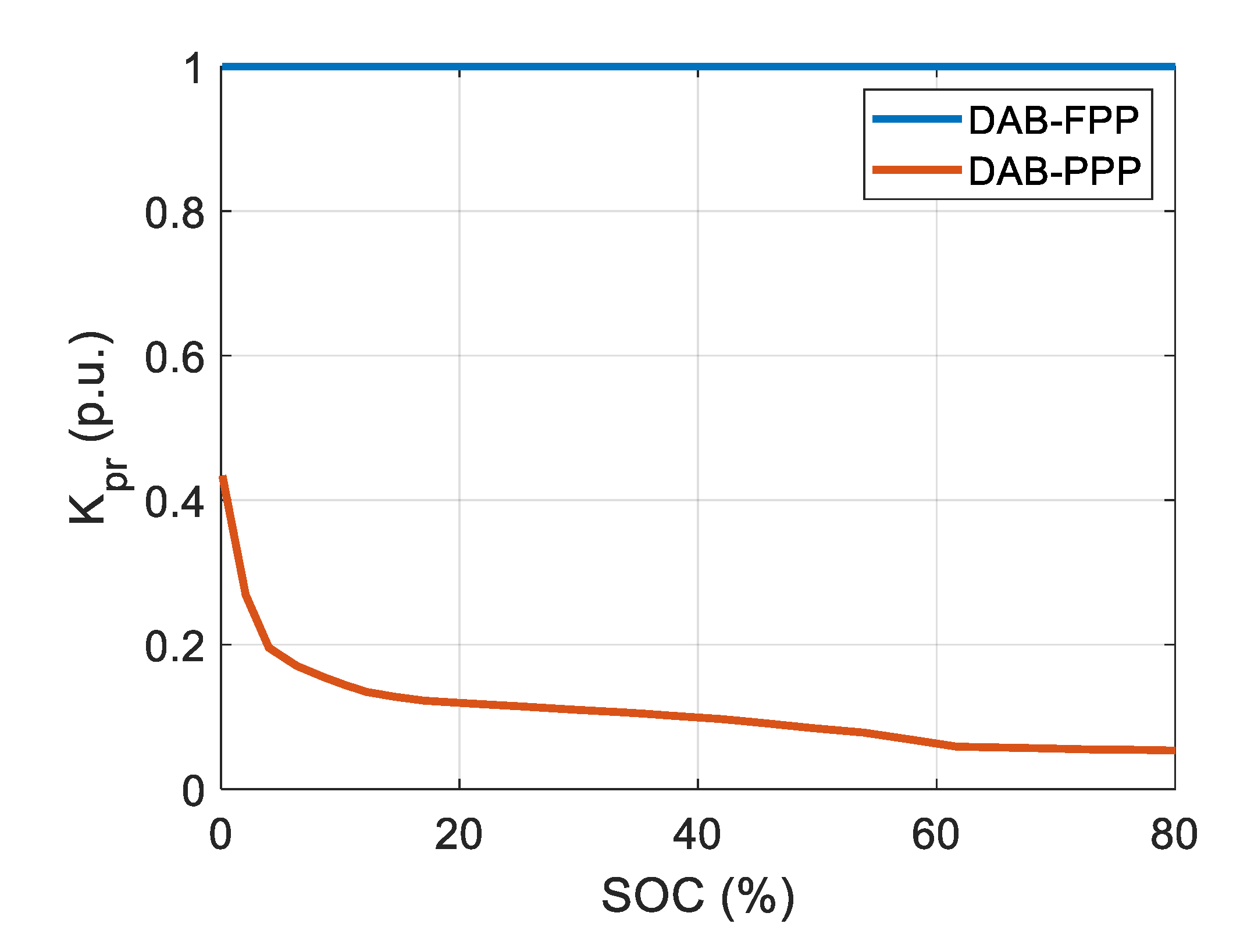
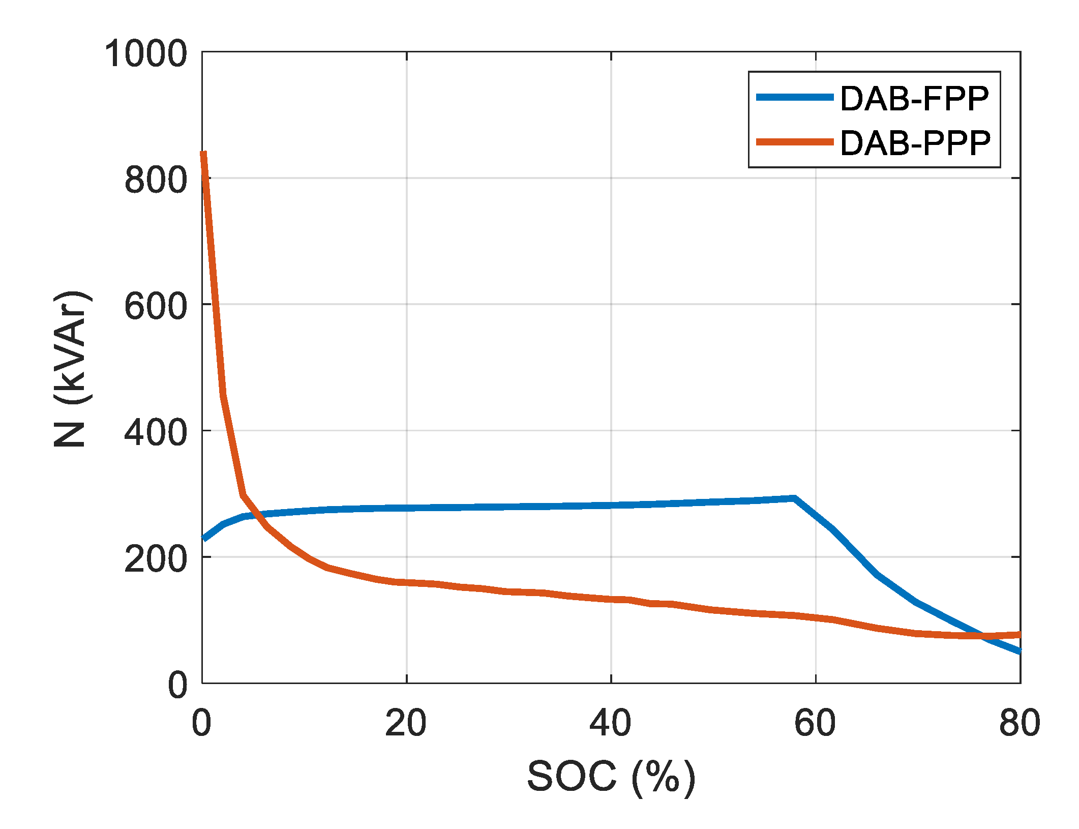
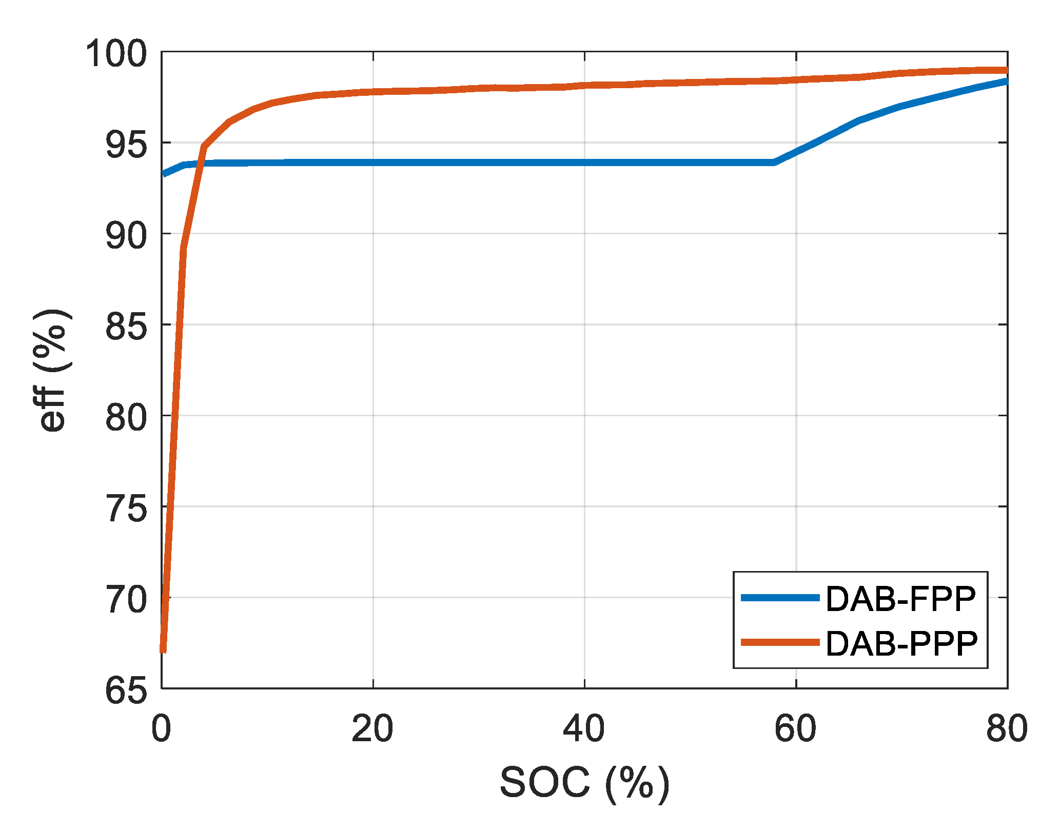
- As observed in Figure 9 and Figure 10, the DAB-PPP presents higher processed non-active power and lower efficiency at initial charging periods. This is due to the fact that power converters inside PPC architectures are required to work at a wider operation range than FPCs [20]. In consequence, lower performance is achieved at extreme working points. In order to improve this, extended analysis on advanced modulation methods is proposed.
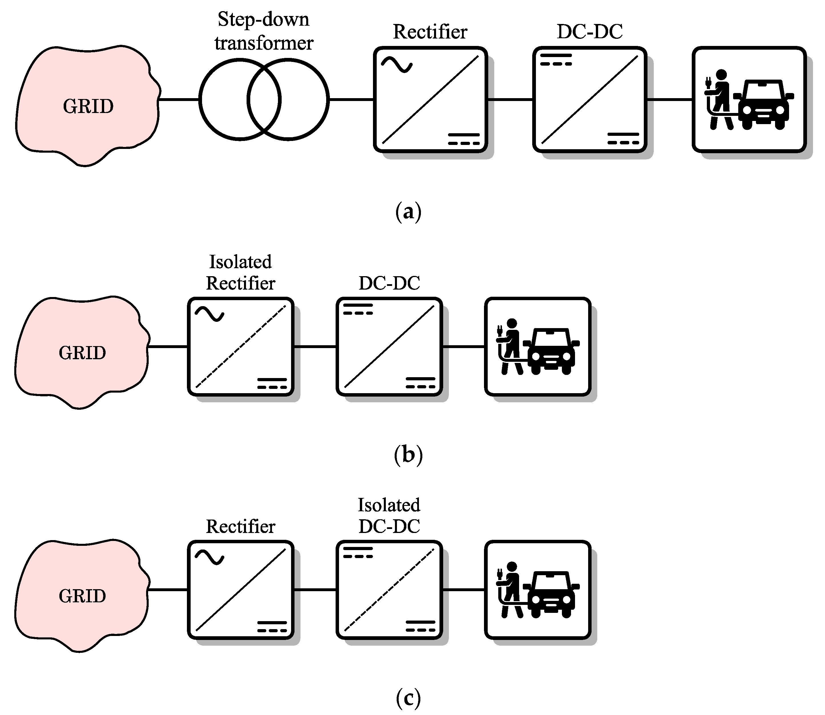
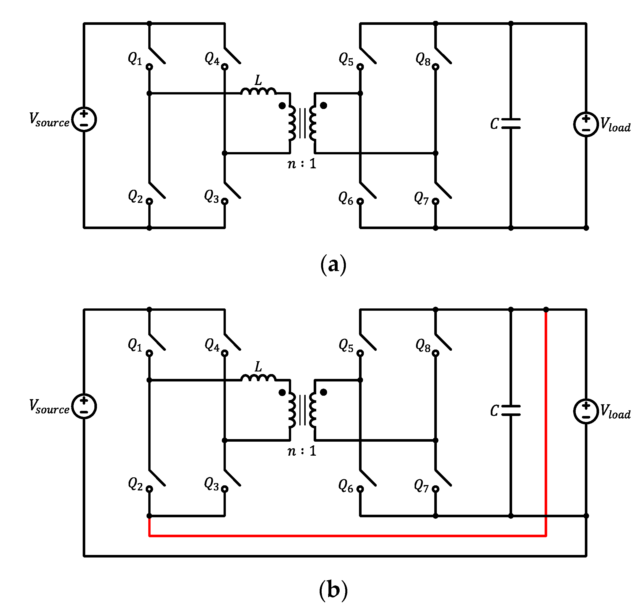
- Although the main objective of the paper is to compare the behavior of a given topology (in this case a DAB) when it is implemented on a FPP architecture and on a PPP architecture, this comparison may not be considered completely fair, since one of the solutions provides galvanic isolation and the other one does not. Therefore, it is proposed to extend the comparison by adding the AC-DC stage. Indeed, as shown in Figure 1, every EV fast charging station consists of an AC-DC and a DC-DC stage and, when it comes to the galvanic isolation, it can be located at one stage or the other. This way, the galvanic isolation can be provided by both solutions: non-isolated AC-DC stage with an isolated DC-DC stage (DAB-FPP) and an isolated AC-DC stage with a non-isolated DC-DC stage (DAB-PPP).
Author Contributions
Funding
Conflicts of Interest
Appendix A

| Description | Reference |
|---|---|
| Source | ITECH IT6012C-800-40 |
| Load | EA-ELR 9750-22 |
| Power meter | YOKOGAWA WT500 |
| Temperature measurement | Pico TC-08 |
References
- Irle, R. EV-Volumes—The Electric Vehicle World Sales Database. 2018. Available online: http://www.ev-volumes.com/ (accessed on 6 March 2019).
- Gorzelany, J. The Longest Range Electric Cars For. 2019. Available online: https://insideevs.com/features/342424/the-longest-range-electric-cars-for-2019/ (accessed on 6 March 2019).
- Dickerman, L.; Harrison, J. A new car, a new grid: The electric car is back (with Help from New Batteries, a Smarter Grid, and Uncle Sam). IEEE Power Energy Mag. 2010, 8, 55–61. [Google Scholar] [CrossRef]
- Christen, D. Analysis and Performance Evaluation of Converter Systems for EV-Ultra-Fast Charging Stations with Integrated Grid Storage. Doctoral Dissertation, ETH Zurich, Zürich, Switzerland, 2017; p. 195. [Google Scholar]
- Etter Place: What Went Wrong for the Electric car Startup? | Environment | The Guardian. Available online: https://www.theguardian.com/environment/2013/mar/05/better-place-wrong-electric-car-startup (accessed on 23 September 2020).
- Bosshard, R.; Badstubner, U.; Kolar, J.W.; Stevanovic, I. Comparative evaluation of control methods for Inductive Power Transfer. In Proceedings of the 2012 International Conference on Renewable Energy Research and Applications (ICRERA), Nagasaki, Japan, 11–14 November 2012. [Google Scholar]
- Chargemap—Electric Cars’ Charging Station Map. Available online: https://chargemap.com/map (accessed on 23 September 2020).
- Iyer, V.M.; Gulur, S.; Gohil, G.; Bhattacharya, S. Extreme fast charging station architecture for electric vehicles with partial power processing. In Proceedings of the 2018 IEEE Applied Power Electronics Conference and Exposition (APEC), San Antonio, TX, USA, 4–8 March 2018; pp. 659–665. [Google Scholar]
- Zapata, J.W.; Kouro, S.; Carrasco, G.; Meynard, T.A. Step-down partial power DC-DC converters for two-stage photovoltaic string inverters. Electronics 2019, 8, 87. [Google Scholar] [CrossRef] [Green Version]
- Zapata, J.W.; Kouro, S.; Carrasco, G.; Renaudineau, H. Step-up partial power DC-DC converters for two-stage PV systems with interleaved current performance. Energies 2018, 11, 357. [Google Scholar] [CrossRef] [Green Version]
- Zientarski, J.R.R.; Martins, M.L.d.; Pinheiro, J.R.; Hey, H.L. Series-Connected Partial-Power Converters Applied to PV Systems: A Design Approach Based on Step-Up/Down Voltage Regulation Range. IEEE Trans. Power Electron. 2017, 33, 7622–7633. [Google Scholar] [CrossRef]
- Mira, M.C.; Zhang, Z.; Jorgensen, K.L.; Andersen, M.A.E. Fractional Charging Converter with High Efficiency and Low Cost for Electrochemical Energy Storage Devices. IEEE Trans. Ind. Appl. 2019, 55, 7461–7470. [Google Scholar] [CrossRef]
- Mishra, S.; Tamballa, S.; Pallantala, M.; Raju, S.; Mohan, N. Cascaded Dual-Active Bridge Cell Based Partial Power Converter for Battery Emulation. In Proceedings of the 2019 20th Workshop on Control and Modeling for Power Electronics (COMPEL), Toronto, ON, Canada, 17–20 June 2019; pp. 1–7. [Google Scholar]
- Pape, M.; Kazerani, M. Turbine Startup and Shutdown in Wind Farms Featuring Partial Power Processing Converters. IEEE Open Access J. Power Energy 2020, 7, 254–264. [Google Scholar] [CrossRef]
- Pape, M.; Kazerani, M. An Offshore Wind Farm with DC Collection System Featuring Differential Power Processing. IEEE Trans. Energy Convers. 2019, 35, 222–236. [Google Scholar] [CrossRef]
- Qin, S.; Barth, C.B.; Pilawa-Podgurski, R.C.N. Enhancing Microinverter Energy Capture with Submodule Differential Power Processing. IEEE Trans. Power Electron. 2014, 31, 3575–3585. [Google Scholar] [CrossRef]
- Kasper, M.; Bortis, D.; Kolar, J.W. Unified power flow analysis of string current diverters. Electr. Eng. 2018, 100, 2085–2094. [Google Scholar] [CrossRef]
- Iyer, V.M.; Gulur, S.; Bhattacharya, S.; Ramabhadran, R. A Partial Power Converter Interface for Battery Energy Storage Integration with a DC Microgrid. In Proceedings of the 2019 IEEE Energy Conversion Congress and Exposition (ECCE), Baltimore, MD, USA, 29 September–3 October 2019; pp. 5783–5790. [Google Scholar]
- Candan, E.; Shenoy, P.S.; Pilawa-Podgurski, R.C.N. A Series-Stacked Power Delivery Architecture with Isolated Converters For Energy Efficient Data Centers. IEEE Trans. Power Electron. 2014, 31, 3690–3703. [Google Scholar] [CrossRef]
- Iyer, V.M.; Gulur, S.; Gohil, G.; Bhattacharya, S. An Approach towards Extreme Fast Charging Station Power Delivery for Electric Vehicles with Partial Power Processing. IEEE Trans. Ind. Electron. 2019, 67, 8076–8808. [Google Scholar] [CrossRef]
- Rojas, J.; Renaudineau, H.; Kouro, S.; Rivera, S. Partial power DC-DC converter for electric vehicle fast charging stations. In Proceedings of the IECON 2017-43rd Annual Conference of the IEEE Industrial Electronics Society, Beijing, China, 29 October–1 November 2017; Volume 2017, pp. 5274–5279. [Google Scholar]
- Buck, J. International electrotechnical commission. Handb. Transnatl. Econ. Gov. Regimes 2016, 573–584. [Google Scholar] [CrossRef]
- Anzola, J.; Aizpuru, I.; Romero, A.A.; Loiti, A.A.; Lopez-Erauskin, R.; Artal-Sevil, J.S.; Bernal, C. Review of Architectures Based on Partial Power Processing for DC-DC Applications. IEEE Access 2020, 8, 103405–103418. [Google Scholar] [CrossRef]
- Zhao, J.; Yeates, K.; Han, Y. Analysis of High Efficiency DC/DC Converter Processing Partial Input/Output Power. In Proceedings of the 2013 IEEE 14th Workshop on Control and Modeling for Power Electronics (COMPEL), Salt Lake City, UT, USA, 23–26 June 2013; pp. 1–8. [Google Scholar]
- Chen, L.; Wu, H.; Xu, P.; Hu, H.; Wan, C. A high step-down non-isolated bus converter with partial power conversion based on synchronous LLC resonant converter. In Proceedings of the 2015 IEEE Applied Power Electronics Conference and Exposition (APEC), Charlotte, NC, USA, 15–19 March 2015; Volume 2015, pp. 1950–1955. [Google Scholar]
- IEEE. IEEE Standard Definitions for the Measurements of Electric Power Quantities Under Sinusoidal, Nonsinusoidal, Balanced or Unbalanced Conditions. Available online: https://pdfs.semanticscholar.org/29a9/36f02016a71ca26ea5d4fa05a2a974984b14.pdf?_ga=2.41965094.2034374545.1611191539-1641229895.1606892986 (accessed on 8 April 2019).


| Parameter | Value | |
|---|---|---|
| DAB-FPP | DAB-PPP | |
| (V) | 400 | 173 ÷ 20 |
| (V) | 227 ÷ 380 | 227 ÷ 380 |
| (p.u.) | 1 | 0.413 ÷ 0.05 |
| (kHz) | 10 | 10 |
| (kW) | 90 | 23.25 |
| 1.0919 | 0.0919 | |
| (µH) | 23.05 | 1.94 |
| Parameter | Value |
|---|---|
| (kW) | 3 |
| (V) | 320 |
| (V) | 220 ÷ 300 |
| Parameter | Value | |
|---|---|---|
| DAB-FPP | DAB-PPP | |
| (V) | 320 | 100 ÷ 20 |
| (V) | 220 ÷ 300 | 220 ÷ 300 |
| (p.u.) | 1 | 0.31 ÷ 0.06 |
| (kHz) | 50 | 50 |
| (kW) | 3 | 0.69 |
| Component | Value | |
|---|---|---|
| DAB-FPP | DAB-PPP | |
| Q1–4 | IPT65R033G7 1 | IPT111N20NFD 2 |
| Q5–8 | IPT65R033G7 | IPT65R033G7 |
| C (µF) | MKP1848C 3 | MKP1848C |
| n | 1.31 | 0.261 |
| L (µH) | 101.5 | 305.34 4 |
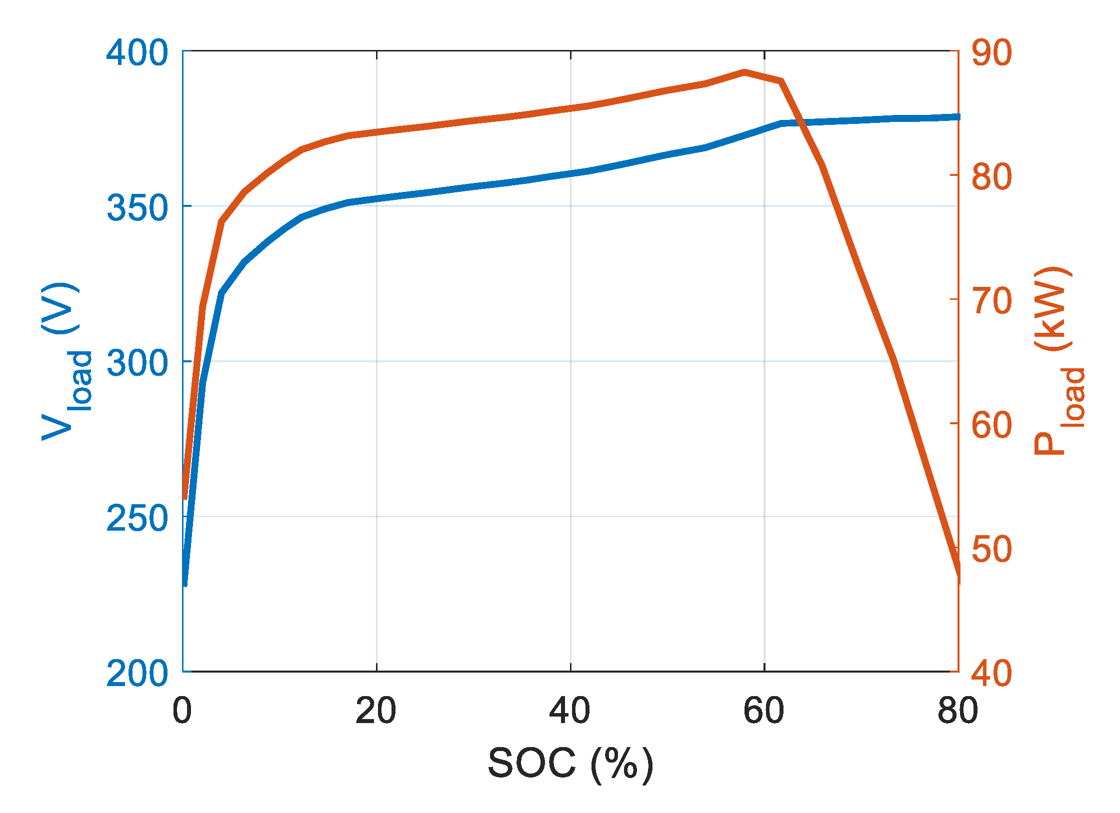
| SOC (%) | Vsourse (V) | Vload (V) | Pload (kW) |
|---|---|---|---|
| 1.5 | 320 | 220 | 2.2 |
| 5.7 | 320 | 260 | 2.6 |
| 60 | 320 | 300 | 3 |
| 80 | 320 | 300 | 1.5 |
| Test Condition | Parameter | Value | |
|---|---|---|---|
| DAB-FPP | DAB-PPP | ||
| Vload = 220 (V) | Psourse (kW) | 2.21 | 2.24 |
| Pin (kW) | 0.699 | ||
| Kpr (p.u.) | 1 | 0.312 | |
| Vload = 260 (V) | Psourse (kW) | 2.58 | 2.53 |
| Pin (kW) | 0.474 | ||
| Kpr (p.u.) | 1 | 0.187 | |
| Vload = 300 (V) SOC = 60% | Psourse (kW) | 3.02 | 2.85 |
| Pin (kW) | 0.176 | ||
| Kpr (p.u.) | 1 | 0.062 | |
| Vload = 300 (V) SOC = 60% | Psourse (kW) | 1.54 | 1.38 |
| Pin (kW) | 0.086 | ||
| Kpr (p.u.) | 1 | 0.062 | |
Publisher’s Note: MDPI stays neutral with regard to jurisdictional claims in published maps and institutional affiliations. |
© 2021 by the authors. Licensee MDPI, Basel, Switzerland. This article is an open access article distributed under the terms and conditions of the Creative Commons Attribution (CC BY) license (http://creativecommons.org/licenses/by/4.0/).
Share and Cite
Anzola, J.; Aizpuru, I.; Arruti, A. Partial Power Processing Based Converter for Electric Vehicle Fast Charging Stations. Electronics 2021, 10, 260. https://doi.org/10.3390/electronics10030260
Anzola J, Aizpuru I, Arruti A. Partial Power Processing Based Converter for Electric Vehicle Fast Charging Stations. Electronics. 2021; 10(3):260. https://doi.org/10.3390/electronics10030260
Chicago/Turabian StyleAnzola, Jon, Iosu Aizpuru, and Asier Arruti. 2021. "Partial Power Processing Based Converter for Electric Vehicle Fast Charging Stations" Electronics 10, no. 3: 260. https://doi.org/10.3390/electronics10030260
APA StyleAnzola, J., Aizpuru, I., & Arruti, A. (2021). Partial Power Processing Based Converter for Electric Vehicle Fast Charging Stations. Electronics, 10(3), 260. https://doi.org/10.3390/electronics10030260