Abstract
Due to commercial restrictions, aiming for greater product competitiveness, uninterruptible power supplies (UPS) must exhibit optimal design in order to reduce losses, volume, and noise, as well as increase power density. However, the optimal design of a power electronic converter is a complex and repetitive task, often requiring the use of a computational tool. The main objective of this work is to present a unified computational tool capable of helping the designer to find the optimal design for a given power electronic converter. This paper will show a comparison between two power converter design techniques: the traditional industrial design approach and a multi-objective optimization approach using Pareto analysis. For this purpose, the total performance of a 10 kVA UPS was compared in terms of losses and volumes. The use of the proposed computational tool to optimize the design resulted in a UPS with better power density and efficiency.
1. Introduction
Electronic power systems have gained increasing relevance in the various economic sectors, as they enable the efficient conversion of energy and add more intelligence and control to the electric generation, transport, and consumption chain. In this context, the use of strategies that allow the development of optimized systems for each application becomes a relevant topic.
The design of power electronic systems, and consequently of converters components that compose them, must meet a series of performance requirements and metrics, whether they are established by standards [1], or because of dynamic restrictions, such as electromagnetic interference (EMI) or total harmonic distortion (THD) or by market demands and application-specific characteristics, e.g., cost, efficiency, and reliability [2]. Obviously, the importance of each metric depends on the type of application [3].
The design of power electronic systems is intrinsically a multi-objective task, where a set of performance requirements are pursued, e.g., power and voltage ratings, dynamic response, standard compliance, and efficiency. However, some figures of merit, efficiency and power density, for instance, are rarely incorporated in the design procedure of converters. On the contrary, those figures are usually assessed a posteriori. The Pareto analysis introduces a more systemic approach to the converter’s design, allowing multiple goals to be addressed and an optimal solution to be found. However, the successful application of this technique by manufacturers requires a unified tool that allows for automatic dimensioning and evaluation of several possible converter designs, for a given performance space.
This article presents the development of a software application capable of helping designers in the multi-objective design of static converters, referred to herein as a multi-objective computational aided design (mCAD) tool. For this work, given the complexity of addressing all possible performance metrics and converter applications, it was decided to direct the application to a reduced set of metrics, namely: efficiency, volume, and weight.
The main purpose of this paper is to describe a unified computational tool that performs a multi-objective design procedure for power electronic converters based on Pareto analysis [4,5,6,7,8]. Unlike other proposals, where generic performance models for components are used to estimate the technological Pareto front for a given converter, the proposed tool relies on brute force computation of all feasible designs for a given database of real components, which delivers a more realistic outcome to be used by manufactures.
Moreover, the paper investigates the benefits of the Pareto analysis design approach in comparison with more traditional converter design methods. Therefore, the design of a 10 kVA UPS is compared, one performed by the proposed tool and the other described in [9].
The remainder of the paper is organized as follows: In Section 2, the procedure performed by the mCAD tool to optimize the UPS design is presented. Section 3 a case study is presented where a 10 kW UPS design is performed using the proposed mCAD tool and this obtained result is compared with a conventional design procedure described in the literature for the same topology and converter specifications. Section 4 concludes this paper by stating the applicability of the proposed tool.
2. Optimization Procedure
The considered optimization procedure for UPS converter designs is based on the Pareto analysis of the power density x efficiency () solution space of all feasible designs for a given set of input requirements. The proposed tool provides an interactive visual plot where the designer can select the design that best suits their objectives.
The mCAD tool takes as input a set of design requirements (voltage and power ratings, converter topology, etc); databases for real components, such as film and electrolytic capacitors, heatsinks, inductor cores, and power switches; and a set of arrays for variable design quantities, e.g., switching frequencies and inductor current ripples.
For each combination of a switching frequency and inductor current ripple, the mCAD tool simulates the converter behavior and calculates all possible design solutions, and then selects the one with the best compromise between power density and efficiency that lies in the solution Pareto front. This solution is then stored and a new combination is assessed. At the end of the input variable sweep, the tool plots the solution space so the designer can select the design that best suits their needs. Figure 1 depicts the flowchart of the proposed mCAD tool.
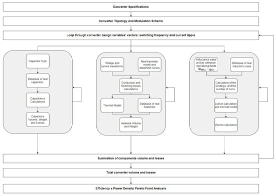
Figure 1.
Flowchart of the local (component level) and global (system level) optimization of a power electronics converter considering the selection and design of the main functional elements of the power circuit. As explained in [7], by neglecting parasitic effects (wiring inductances, electromagnetic and thermal coupling of components, etc.) component designs are largely decoupled and/or individual local optimizations can be carried out; only the component values, the switching frequency , and the ripple current are then determined by an outer global optimization loop.
Initially, the design parameters, the converter topology, and the control scheme are defined. Then, the designer determines the current ripple and switching frequency vectors.
Then, with the parameters and initial variables defined, the component loops (local loops) are entered. In these local loops, all possible design alternatives are simulated, given the database selected. In the following subsections, each local loop will be explained in detail.
2.1. DC Link Calculations
For the correct sizing of the DC link capacitors, a ripple criterion was chosen; that is, the capacitor will be selected in such a way that the maximum ripple voltage does not exceed the specified value.
As explained in [10], when operating with an unbalanced load, a second harmonic current will circulate on the DC link. The greater the imbalance, the greater the ripple. The instantaneous value of this current is presented by (1) [10].
where is the peak value of voltage in phase a; is the peak neutral current; is the angular frequency; is the neutral current phase angle. The voltage on the capacitor is then given by the integral of the current, as shown in (2).
where C is the total capacitance value and F is the grid frequency. Additionally, it can be observed that the voltage on the capacitor will have its maximum value when the sine function is equal to 1. Replacing the value of C with , each capacitor’s group is obtained for the positive and negative bus, as shown in (3).
where is the voltage variation across the capacitor. The neutral current is equal to the vectorial sum of the phase currents, so in the worst case, two phases have currents equals to zero, then the peak value of the neutral current is equal to the maximum peak value of the output current of the inverter [11].
The DC link total volume was calculated considering the volume of a single capacitor, multiplied by the number of capacitors used to form the complete bank (positive and negative bus). The volume of a capacitor is described by (4), where is the height of the capacitor and is its diameter.
For the local capacitor’s loop, first, we choose the capacitor’s type and it is given a database of real capacitors. Then, the required capacitance for the DC link is calculated. Next, the volume of each model in the database is calculated. With the values of and the rated voltage allowed for each capacitor, it is possible to determine the number of capacitors in series that will be necessary. Additionally, with the current circulating the capacitor, given by (1) when the cosine function is equal to 1, and with the rated current of each capacitor , it is possible to define the number of parallel capacitors. The total number of capacitors in the DC link will be the product of the number of capacitors in series and in parallel.
The total losses of the DC link are obtained by solving the equivalent circuit, considering the parasitic series resistance () of each capacitor and the total current. The total volume is then calculated by multiplying the total amount of capacitors found by the unit volume (4). Such calculations are made for all possible options—the different models in the database.
Choosing the best configuration for the DC link is based on a figure of merit (FOM) given by (5). Here, each possibility already calculated has its figure of merit value, and the one whose is the highest will be the chosen option.
2.2. Power Switch Calculations
The conduction power losses in one transistor () and in one diode () are defined as an average of the product between the instantaneous value of the current and voltage. By approximating the integral operator by the finite sum, we have, as described in [12], used (6) and (7) to calculate these losses.
where and denote, in this order, the current through a transistor and through a diode in the k-th sample, whereas and refer to the voltage across transistors and diodes, derived from lookup table outputs.
The switching losses of a transistor and a diode are calculated with (8) and (9), where is given by (10) and is given by (11). Additionally, is given by (12) and is given by (13).
the subscript “REF” indicates the values under which the curves available in datasheets are defined.
The semiconductor losses were calculated using the proposed tool presented in [12], which applies all these formulas to a given power switch and given waveforms that were previously simulated. This software outputs several files, one for each frequency and ripple, with all the information about the power switch losses.
2.3. Heatsink Calculations
It is extremely important in power electronics to understand the effects of temperature in a system and how it affects many aspects of a converter design such as, for example, the choice of components, reliability, performance, robustness, and the volume [13]. As presented in [14], in the literature there are different techniques for thermal modeling of the converter components: analytical, numerical, and analogical modeling with electrical circuits. For the performance analyses proposed in this work, the electro-thermal steady-state models are sufficient.
These models macroscopically describe the thermal behavior of the device and can be derived directly from the data reported in the manufacturer’s catalog [12,15]. In general, thermal circuits are based on the analogy with electrical circuits, where the dissipated power P corresponds to the electrical current, while the temperature difference is mapped as an electric voltage. Therefore, the thermal resistance is given by (14).
where d is the thickness of the material; is the thermal conductivity; A is the cross-sectional area.
The manufacturer’s datasheet generally informs the thermal resistances between the junction and the case () and between the case and the heatsink (), however, this last one may not always be present. If this is the case, as described in [15], is calculated using (14), considering a fiberglass-based “thermal adhesive” of polymeric material, from the manufacturer Bergquist, model GAP PAD 5000S35, of thermal conductivity of thickness d of 0.508 mm, and considering the area A as the available area of the device for heat exchange.
As summarized in [12], with the system elements modeled by conveniently arranged thermal resistances, the junction temperature for each device can be estimated from the equivalent thermal circuit solution. This thermal modeling technique is adopted in this work as an alternative to the analytical and numerical approaches, as it is based only on parameters given in the datasheets.
The mCAD tool uses a function developed in this work to calculate the heatsink design. It receives as input data information about the losses of semiconductor devices (described in the previous subsection), the configuration desired by the user, the maximum acceptable junction temperature, and the ambient temperature. Additionally, this function receives the heatsink database—with information about real models, their widths, heights, and their standard thermal resistances; as well as the temperature and length adjustment curves.
With this information, the heatsink temperature is calculated, following formula (15). According to the configuration, the heatsink temperature is calculated considering the losses and resistances of each component connected to it, and the lowest among them is selected. Such a choice is made because the component that needs a lower heatsink temperature, in order to keep the junction temperature within the limits, is considered the critical element.
Then, the thermal resistance required for the heatsink is calculated according to the number of heatsinks and switches on each one, as shown in (16).
where N is the number of switches per heatsink; is room temperature; and are the losses of a transistor and a diode, respectively. With this information, an adjustment of the necessary thermal resistance is made, according to the temperature calculated by (15). The dissipation by convection depends on the difference between the ambient temperature and the temperature of the air film that surrounds the heatsink. Heatsinks are more efficient when the ambient temperature is low and, as the ambient temperature increases, the efficiency of the heat exchange between the heatsink and the environment deteriorates.
To make this adjustment, interpolation is made between the curve presented in the heatsink datasheet and the value of calculated by (15). We have the temperature correction factor by (17). Then, we calculate the new thermal resistance required for the heatsink according to the formula (18).
Another interpolation is made between the curve , also presented in the datasheet, with the required heatsink resistance value. With this, the minimum length for each heatsink model is found. Here the length found is the minimum, as such length provides the calculated thermal resistance, but any resistance smaller than it keeps the junction temperature of the switch within the limits imposed by the user; also, the longer the length, the lower the resistance.
With the information on the length, height, and width of each heatsink, the volume of all available models is calculated according to (19), for each point
Then, for each point , we obtain the smallest calculated volume and the model of the heatsink.
2.4. Inductors Calculations
Inductors can make up most of the losses and volume of a static converter. Thus, an optimized design methodology for the inductors is of paramount importance.
The total losses in the inductors are the result of the sum of two parts: the losses in the conductors (Joule effect), and the losses in the core as a result of the hysteresis losses, by the Foucault effect and residuals. Two phenomena, known as the skin effect and proximity effect, determine the current distribution along the conductor cross-section for each frequency, and thus, the resistance of the winding [12,16].
As exemplified in [16], due to the skin effect, the current density at the center of the conductor decreases significantly with increasing frequency, which translates into an increase in resistance per conductor length. The proximity effect, as explained in [17], refers to the influence of alternating currents in a conductor on the current distribution in another nearby conductor.
Generally, as shown in [16], the power dissipated in the inductor windings (), with distorted currents, can be estimated by the algebraic sum of the ohmic losses associated with the harmonics of order n, as presented in (20).
where and are the winding resistances for the continuous and alternating components, given that includes the skin and proximity effects, according to [18]; and the peak values of direct and alternating currents. In this work, as well as in [16], skin and proximity effects will be considered since for high-performance static converters such effects are of certain importance.
Classically, to estimate the losses in the magnetic cores of the inductors, we the Steinmetz equation [16,19], shown in (21).
where k, , and are constants informed by the core manufacturer and that depend on the material properties; denotes the value of peak flux density, and is the volume of the core. However, this equation only applies to sinusoidal excitation and is not accurate for modeling static converters with PWM modulation (pulse-width modulation) [16,19].
Core losses will be estimated using the method iGSE (improved generalized Steinmetz equation) given by (22), with indicated by (23), as proposed in [20].
where refers to the peak-to-peak excursion of flux density B with period T (inverse of the fundamental frequency F of the current in the inductor); the constants k, , and are the same as in the Steinmetz equation (Equation (21)) and the angle refers to the instantaneous angle of B.
The volume of an inductor is calculated considering the toroidal core. The area of the circular ring is calculated (considering the outer radius minus the inner radius) and then multiplied by the height of the core. Then add to that the volume of the copper wires, and then multiply it by the number of inductors.
The inductor’s losses, volumes, and weight were calculated using the proposed tool presented in [16]. This tool considers the voltage, current, and frequency imposed on the inductor in order to define the core and winding necessary to obtain the required inductance value. Losses and temperature rise are also estimated during inductor operation while respecting the limits of saturation, temperature, and core filling. Furthermore, the effect of non-idealities, such as the skin effect and the proximity effect, as well as the effects caused by a non-sinusoidal excitation in the windings, were incorporated into the inductor design.
Among the possible designs of a single inductor, obtaining the one whose characteristics are closest to the desired is not a trivial task, since the number of variables is large, in addition to the different phenomena acting simultaneously. It is necessary to carry out the design of an inductor repeatedly and compare the results so that it is possible to identify the best design for each situation.
In the core losses calculations, the iGSE equation (Equation (22)) is used, which makes use of the vector B(t) obtained from the voltage vector. With this, the losses are calculated for any waveform, only with the parameters of the Steinmetz equation (Equation (21)).
To compose the final mCAD tool proposed here, the software developed in [16] was modified. It was inserted into a loop in order to define all the inductors for a given point and for all available materials. With this, being the size of the current ripple array, the size of the switching frequency array, and the amount of materials available in the database, one has inductor reports.
Based on the inductor reports, the optimization for each point is made—that is, the best material is chosen for each point. This local optimization was done based on the analysis developed in [7] and is briefly explained here: when the component design becomes decoupled, individual local optimizations can be performed.
2.5. Full Converter Calculations
Finally, all previous data is combined, adding to the total system’s losses the losses of the inductors, capacitors, and semiconductor devices, as shown in (24); the volume of the heatsink and the inductors is added to the total volume (shown in (25)).
However, as described in [7], when each component’s volume (individual volume—) is calculated separately, it is necessary to adjust the total volume of the converter () to consider the different geometries of the components. For this, the (26) is used.
According to [7], the coefficient varies between 0.5 and 0.7. While larger values can be achieved by adapting the geometries of the components, for this work, a coefficient of 0.6 was chosen. Therefore, to calculate the final total volume of the converter, the mCAD tool makes the adjustment by a factor of 0.6, as shown in (25).
Thus, the efficiency () can be calculated based on the output power () and the total system losses (), as in (27). Additionally, the power density () is calculated based on the output power and the total volume, as in (28).
Finally, each point is plotted in a curve, forming a Pareto Front with the best designs of each frequency and ripple data point. It is then up to the designer to analyze such curves and, finally, choose the point that best meets the project’s requirements.
3. Results
To show the applicability of the mCAD tool, a case study was selected to compare the traditional converter design method with the computational tool (using Pareto analysis) proposed by this article.
A hybrid AC-DC-AC UPS converter described in [9] and [21] shown in Figure 2 was chosen. It consists of a Vienna rectifier at the input and a two-level inverter at the output. A silicon carbide device, SCT3030AL, was used. Table 1 shows the design parameters used for analysis. This topology and the UPS specifications were selected based on the comparison presented in [9].
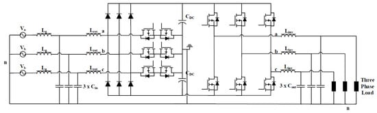
Figure 2.
Hybrid AC-DC-AC converter used as the subject of case studies for the software developed in this article.

Table 1.
Design parameters.
The frequency chosen by [9] for the rectifier was 102 kHz, and 101.34 kHz for the inverter. A current ripple of 40% and 30% was chosen for the inverter and rectifier, respectively. Additionally, an efficiency of 95% was reached for the complete UPS. The results of this UPS design are shown in Table 2. Table 3 presents the data of the UPS designed by the mCAD tool.
Table 2.
Requirements and design criteria for the UPS from [9].
Table 3.
Requirements and design criteria for the UPS using the proposed mCAD tool.
Figure 3 and Figure 4 illustrate the results obtained by the mCAD tool. Pareto curves () for the rectifier and inverter are presented. An optimal point was chosen by the user in order to obtain the optimized UPS. The optimal points chosen through the optimization software are presented, as well as the points of the converter in [9]. It is important to note that the mCAD tool simulates design possibilities given a database of real components. Therefore, it has a discrete number of possibilities. With the given database, the Pareto fronts presented in Figure 3 and Figure 4 were obtained. Analyzing these figures, it is possible to note that there is no trade-off for a better part of the design’s results—several options have worse power density and efficiency. This is explained because, with this database, the mCAD tool could not find better solutions for these points. When increasing the component database with new and better models, other design points will appear in the Pareto Front, and possibly, change the curve’s shape.
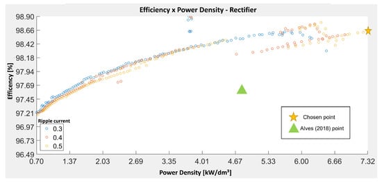
Figure 3.
Pareto front () for the rectifier.
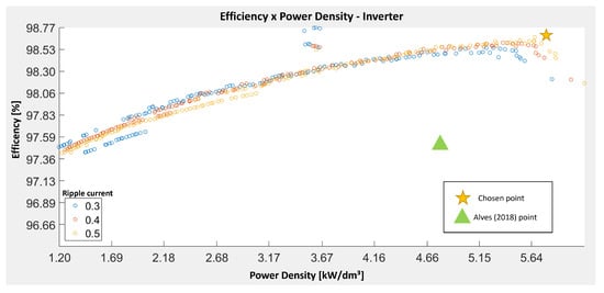
Figure 4.
Pareto front () for the inverter.
The UPS designed with the mCAD tool reached a power density of 3.22 kW/dm³ with an efficiency of 97.36%, both metrics are superior to those achieved in [9]. Therefore, it can be seen that with the aid of the optimization tool it was possible to design a UPS with greater efficiency and power density.
Table 4 presents a comparison between the converter proposed by [9] and the one proposed by the mCAD tool. As [9] does not present the individual information of the converters separately, it was considered, for the purpose of comparison, that the inverter and the rectifier had equal efficiency, weights, and volumes.
Table 4.
Comparison of components’ weight and volume and UPS’s power density and efficiency for the designs obtained with the mCAD tool and with the one developed in [9].
It is important to note that the frequency selected by the mCAD tool was well below the one defined by [9], −14.40 kHz against 101.34 kHz for the inverter and 20.16 kHz against 102 kHz for the rectifier, even though the same power electronic switch was considered. An explanation for this is the fact that with the increase in frequency, the losses in the switches increase considerably, and, consequently, a larger heatsink is required in order to dissipate all this generated heat. The decrease in passive elements—inductors and capacitors—does not compensate for the increase in the heatsink.
It can be seen that the mass and volume of the inductors are considerably smaller for cases whose switching frequency is higher. For example, for the inverter in [9], with a frequency of 101.34 kHz, the inductor’s mass was 255.00 g, and its volume was 35.30 cm. However, when the switching frequency is reduced to 14.40 kHz, the inductor mass increases to 1183.80 g (an increase of approximately 360%), and the volume becomes 156.80 cm (an increase of approximately 340%). As for the rectifier, the difference was smaller. For 20.16 kHz, the inductor mass was 612.40 g (an increase of approximately 140%) and the volume was 84.00 cm (an increase of approximately 140%).
However, this difference is inverted when analyzing the heatsinks. A frequency of 101.34 kHz used a heatsink whose mass was 2350.00 g, and a volume of 1612.50 cm. By reducing the frequency to 14.40 kHz, it was possible to use a considerably smaller heatsinks, with a mass of 422 g (a reduction of approximately 82%), and with a volume of 319.61 cm (reduction of approximately 80%). The same happened with the inverter.
Figure 5 and Figure 6 were plotted with the same component database. It shows that by increasing the switching frequency, the volume and weight of the inductor decrease, while the heatsink, on the other hand, increases both in volume and weight as the frequency increases. It can be seen that the increase in the heatsink volume is greater than the decrease in inductor volume. Therefore, as the frequency increases, the decrease in the inductor volume does not compensate for the increase in the heatsink volume.
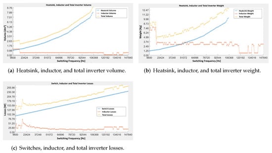
Figure 5.
Inverter volume, weight, and loss curves.
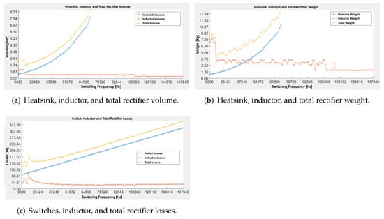
Figure 6.
Rectifier volume, weight, and loss curves.
These differences resulted in a power density of 2.35 kW/dm and an efficiency of 95.00% in the UPS designed in [9] against a power density of 3.22 kW/dm and an efficiency of 97.36% for the proposed optimized UPS.
4. Conclusions
The mCAD tool proved to be very useful for optimal power converters design. Instead of individually simulating each design option, as is done in traditional design methods, with the mCAD tool the designer has a visual outcome of the various design possibilities based on their component database and can then select the one that best suits their objectives. The mCAD tool allows the designer to test different cases easily. With it, it is possible to evaluate several distinct scenarios. Additionally, with the mCAD tool, the relationship between efficiency and power density for the given database can be analyzed easily.
The case study showed consistent results and the numbers in Table 4 showed that it was possible to design a UPS with greater power density and efficiency using the proposed approach in comparison with traditional design methods.
It is important to note that the proposed design used a database of real components as input, which means that the Pareto front plotted by the optimization tool is not theoretical, all designs are applicable and can be used by manufacturers. In addition, it is possible to increase the component database to expand the optimization possibilities.
Author Contributions
Conceptualization, P.A.d.C.eC., L.M.F.M. and T.R.d.O.; methodology, P.A.d.C.eC., L.M.F.M. and T.R.d.O.; software, P.A.d.C.eC.; validation, P.A.d.C.eC., L.M.F.M. and T.R.d.O.; formal analysis, P.A.d.C.eC., L.M.F.M. and T.R.d.O.; investigation, P.A.d.C.eC., L.M.F.M. and T.R.d.O.; resources, L.M.F.M. and T.R.d.O.; data curation, P.A.d.C.eC., L.M.F.M. and T.R.d.O.; writing—original draft preparation, P.A.d.C.eC.; writing—review and editing, P.A.d.C.eC., L.M.F.M. and T.R.d.O.; visualization, P.A.d.C.eC., L.M.F.M. and T.R.d.O.; supervision, L.M.F.M. and T.R.d.O.; project administration, L.M.F.M. and T.R.d.O.; funding acquisition, L.M.F.M. and T.R.d.O. All authors have read and agreed to the published version of the manuscript.
Funding
This study was financed in part by the Coordenação de Aperfeiçoamento de Pessoal de Nível Superior—Brasil (CAPES)—Finance Code 001.
Data Availability Statement
Not applicable.
Acknowledgments
The authors would like to thank the Programa de Pós Graduação em Engenharia Elétrica da Universidade Federal de Minas Gerais (PPGEE-UFMG) for the financial support given for the publication of this paper.
Conflicts of Interest
The authors declare no conflict of interest.
References
- International Electrotechnical Commission. IEC 62040: Uninterruptible Power Systems (UPS)-Part 3: Method of Specifying the Performance and Test Requirements. Int. Stand. IEC 2021. Available online: https://webstore.iec.ch/preview/info_iec62040-3%7Bed1.0%7Den_d.pdf (accessed on 1 September 2022).
- Kolar, J.W.; Drofenik, U.; Biela, J.; Heldwein, M.L.; Ertl, H.; Friedli, T.; Round, S.D. PWM converter power density barriers. In Proceedings of the 2007 Power Conversion Conference-Nagoya, Nagoya, Japan, 2–5 April 2007; p. 9. [Google Scholar]
- Burkart, R.M.; Kolar, J.W. Advanced Modeling and Multi-Objective Optimization/Evaluation of SiC Converter Systems. In Proceedings of the Tutorial at the 3rd IEEE Workshop on Wide Bandgap Power Devices and Applications (WiPDA 2015), Blacksburg, VA, USA, 2–4 November 2015; pp. 2–5. [Google Scholar]
- Biela, J.; Kolar, J.W. Pareto-optimal design and performance mapping of telecom rectifier concepts. In Proceedings of the Power Conversion and Intelligent Motion Conference, Shanghai, China, 1–3 June 2010; pp. 1–13. [Google Scholar]
- Kolar, J.W.; Biela, J.; Minibock, J. Exploring the pareto front of multi-objective single-phase PFC rectifier design optimization-99.2% efficiency vs. 7kW/din 3 power density. In Proceedings of the 2009 IEEE 6th International Power Electronics and Motion Control Conference, Wuhan, China, 17–20 May 2009; pp. 1–21. [Google Scholar]
- Uemura, H.; Krismer, F.; Okuma, Y.; Kolar, J.W. (ρ−η) Pareto optimization of 3-phase 3-level T-type AC-DC-AC converter comprising Si and SiC hybrid power stage. In Proceedings of the 2014 International Power Electronics Conference (IPEC-Hiroshima 2014-ECCE ASIA), Hiroshima, Japan, 18–21 May 2014; pp. 2834–2841. [Google Scholar]
- Kolar, J.W.; Biela, J.; Waffler, S.; Friedli, T.; Badstübner, U. Performance trends and limitations of power electronic systems. In Proceedings of the 2010 6th International Conference on Integrated Power Electronics Systems, Nuremberg, Germany, 16–18 March 2010; pp. 1–20. [Google Scholar]
- Barrera-Cardenas, R.; Molinas, M. A simple procedure to evaluate the efficiency and power density of power conversion topologies for offshore wind turbines. Energy Procedia 2012, 24, 202–211. [Google Scholar] [CrossRef][Green Version]
- Alves, W.C.; Morais, L.M.; Cortizo, P.C. Design of an highly efficient AC-DC-AC three-phase converter using SiC for UPS applications. Electronics 2018, 7, 425. [Google Scholar] [CrossRef]
- Fraser, M.E.; Manning, C.D.; Wells, B.M. Transformerless four-wire PWM rectifier and its application in AC-DC-AC converters. IEE Proc.-Electr. Power Appl. 1995, 142, 410–416. [Google Scholar] [CrossRef]
- da Alves, W.C. Desenvolvimento de uma UPS Trifásica de Alto Rendimento Utilizando Mosfets de Carbeto de Silício; Dissertação (Mestrado em Engenharia Elétrica), Universidade Federal de Minas Gerais: Belo Horizonte, Brazil, 2016; p. 152. [Google Scholar]
- Cota, A.P.; Abrantes, R.C.; Cortizo, P.C.; Santana, R.A.; Padrao, W.C. Comparison of three 3-phase converter topologies for ups applications. In Proceedings of the 2015 IEEE 13th Brazilian Power Electronics Conference and 1st Southern Power Electronics Conference (COBEP/SPEC), Fortaleza, Brazil, 29 November–2 December 2015; pp. 1–6. [Google Scholar]
- Wilson, P.R. Thermal modeling and analysis of power electronic components and systems. In Power Electronics Handbook; Butterworth-Heinemann: Oxford, UK, 2018; pp. 1441–1450. [Google Scholar]
- Shahjalal, M. Electric-Thermal Modelling of Power Electronics Components. Doctoral Dissertation, University of Greenwich, London, UK, 2018. [Google Scholar]
- Santana, R.Á.S. Projeto e análise de rendimento de uma UPS monofásica de três braços e construção de um calorímetro fechado de dupla caixa. Master Thesis, Programa de Pós-graduação em Engenharia Elétrica, UFMG, Belo Horizonte, Brazil, 2018. Available online: https://www.ppgee.ufmg.br/defesas/1513M.PDF (accessed on 1 September 2022).
- Vilkn, P.H.J.; Morais, L.M.F.; Santana, R.A.S.; Cortizo, P.C.; Seixas, P.F. Inductor Design Methodology for Power Electronics Applications. In Proceedings of the 2019 IEEE 15th Brazilian Power Electronics Conference and 5th IEEE Southern Power Electronics Conference (COBEP/SPEC), Santos, Brazil, 1–4 December 2019; pp. 1–6. [Google Scholar]
- Popovic, Z.; Popovic, B.D. Introdutory Eletromagnetics: Practice Problems and Labs. Ph.D. Thesis, Cambridge University Press, Cambridge, MA, USA, 2012; pp. 382–392. [Google Scholar]
- Kondrath, N.; Kazimierczuk, M.K. Inductor winding loss owing to skin and proximity effects including harmonics in non-isolated pulse-width modulated dc–dc converters operating in continuous conduction mode. IET Power Electron. 2010, 3, 989–1000. [Google Scholar] [CrossRef]
- Li, J.; Abdallah, T.; Sullivan, C.R. September. Improved calculation of core loss with nonsinusoidal waveforms. In Proceedings of the Conference Record of the 2001 IEEE Industry Applications Conference. 36th IAS Annual Meeting (Cat. No. 01CH37248), Chicago, IL, USA, 30 September–4 October 2001; Volume 4, pp. 2203–2210. [Google Scholar]
- Venkatachalam, K.; Sullivan, C.R.; Abdallah, T.; Tacca, H. Accurate prediction of ferrite core loss with nonsinusoidal waveforms using only Steinmetz parameters. In Proceedings of the 2002 IEEE Workshop on Computers in Power Electronics, Proceedings, Mayaguez, PR, USA, 3–4 June 2002; pp. 36–41. [Google Scholar]
- Alves, W.C.; Morais, L.M.; Cortizo, P.C. Design of an efficient hybrid AC-DC-AC converter using silicon carbide for ups applications: A comparison. In Proceedings of the 2017 Brazilian Power Electronics Conference (COBEP), Juiz de Fora, Brazil, 19–22 November 2017; pp. 1–6. [Google Scholar]


Publisher’s Note: MDPI stays neutral with regard to jurisdictional claims in published maps and institutional affiliations. |
© 2022 by the authors. Licensee MDPI, Basel, Switzerland. This article is an open access article distributed under the terms and conditions of the Creative Commons Attribution (CC BY) license (https://creativecommons.org/licenses/by/4.0/).