
Developing PCM-Based Microwave and Millimetre-Wave Switching Networks by Optimised Building Blocks

Abstract
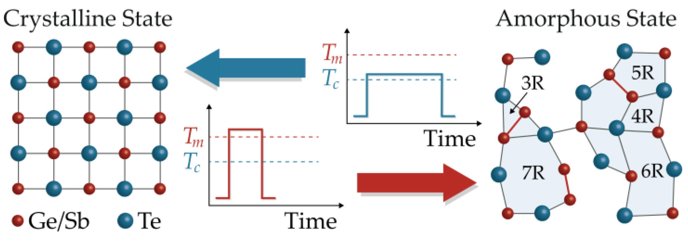
:1. Introduction
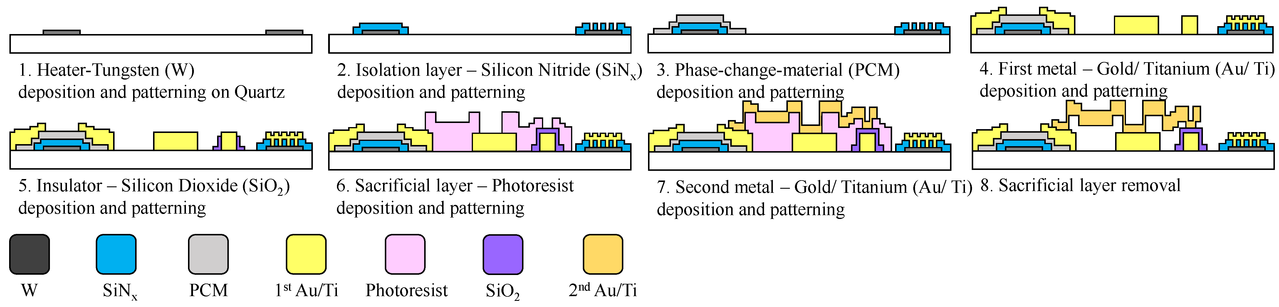
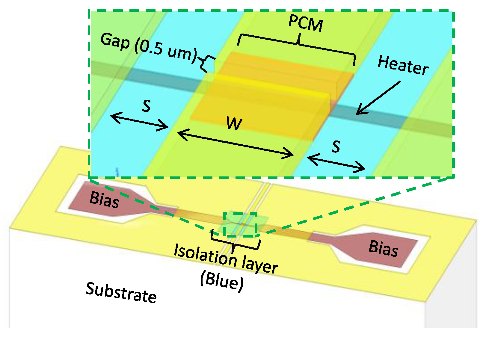
2. Fabrication Process
- A resistive layer used for PCM’s microwave resistors or heaters is deposited and patterned. A 70 nm layer of tungsten (W) is sputtered at 850 °C and patterned using reactive ion etching (RIE);
- A thin isolation/barrier layer of 50 nm silicon nitride (SiNx) is deposited by plasma-enhanced chemical vapour deposition (PECVD);
- A thin PCM layer is deposited. A 150 nm thick PCM is DC sputtered and patterned using the lift-off technique, followed by an annealing process;
- The first RF metal layer, 1 μm of gold (Au) layer, is DC sputtered together will 50 nm of titanium (Ti) for better adhesion. A lift-off process is used to pattern these;
- A second isolation layer, silicon dioxide (SiO2), primarily for MIM capacitors, is PECVD deposited, followed by patterning with diluted hydrofluoric acid (HF). HF is selected to remove the SiO2 as it etches SiO2 at a much higher rate than the previously deposited SiNx and all other materials exposed at the surface;
- A sacrificial layer, polyimide, of 2.5 μm is spun on, patterned, and baked;
- A second RF metal layer (Au/Ti) is DC sputtered and patterned by the lift-off technique. This RF signal layer is primarily for airbridges and MIM capacitors.
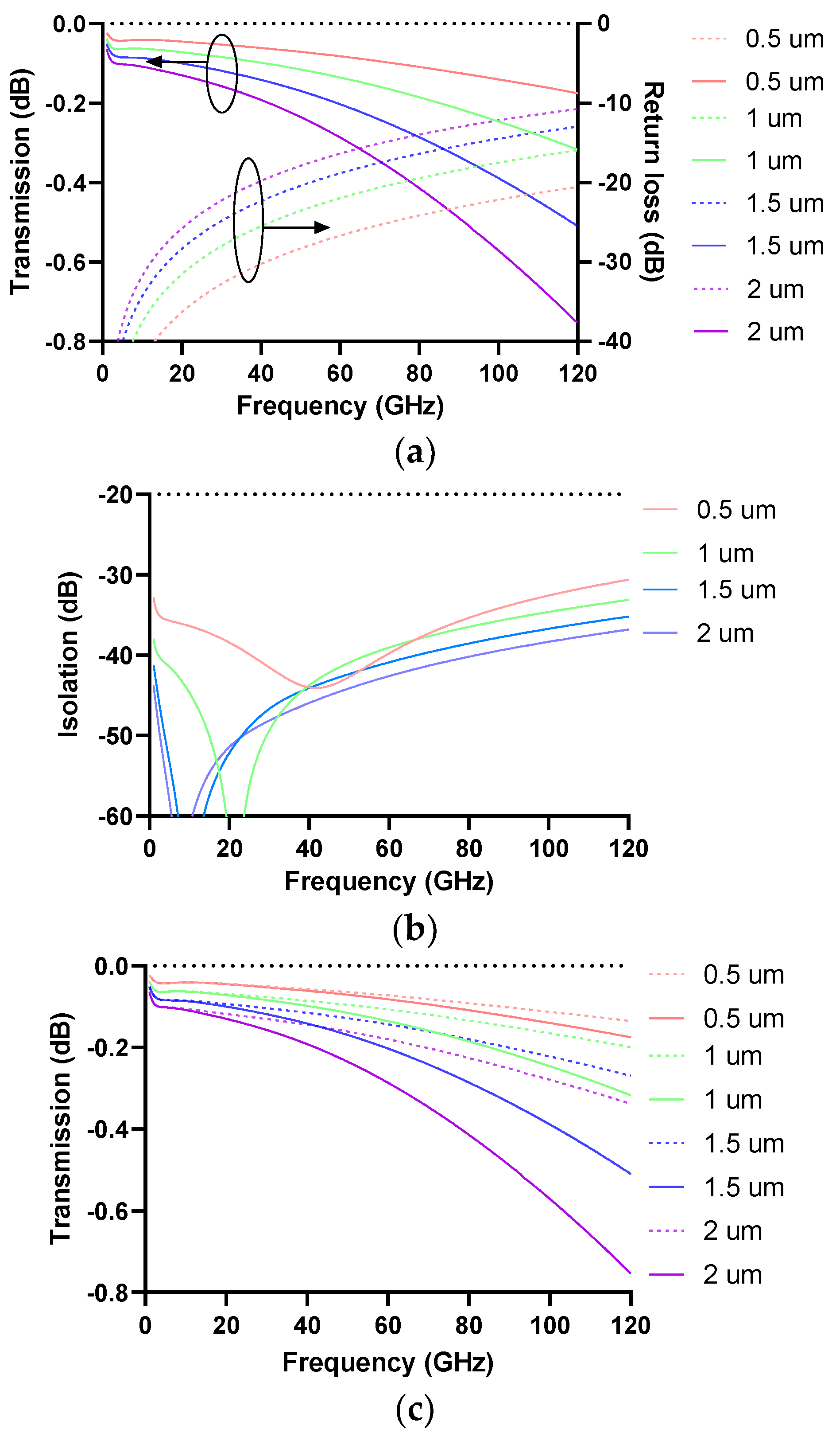
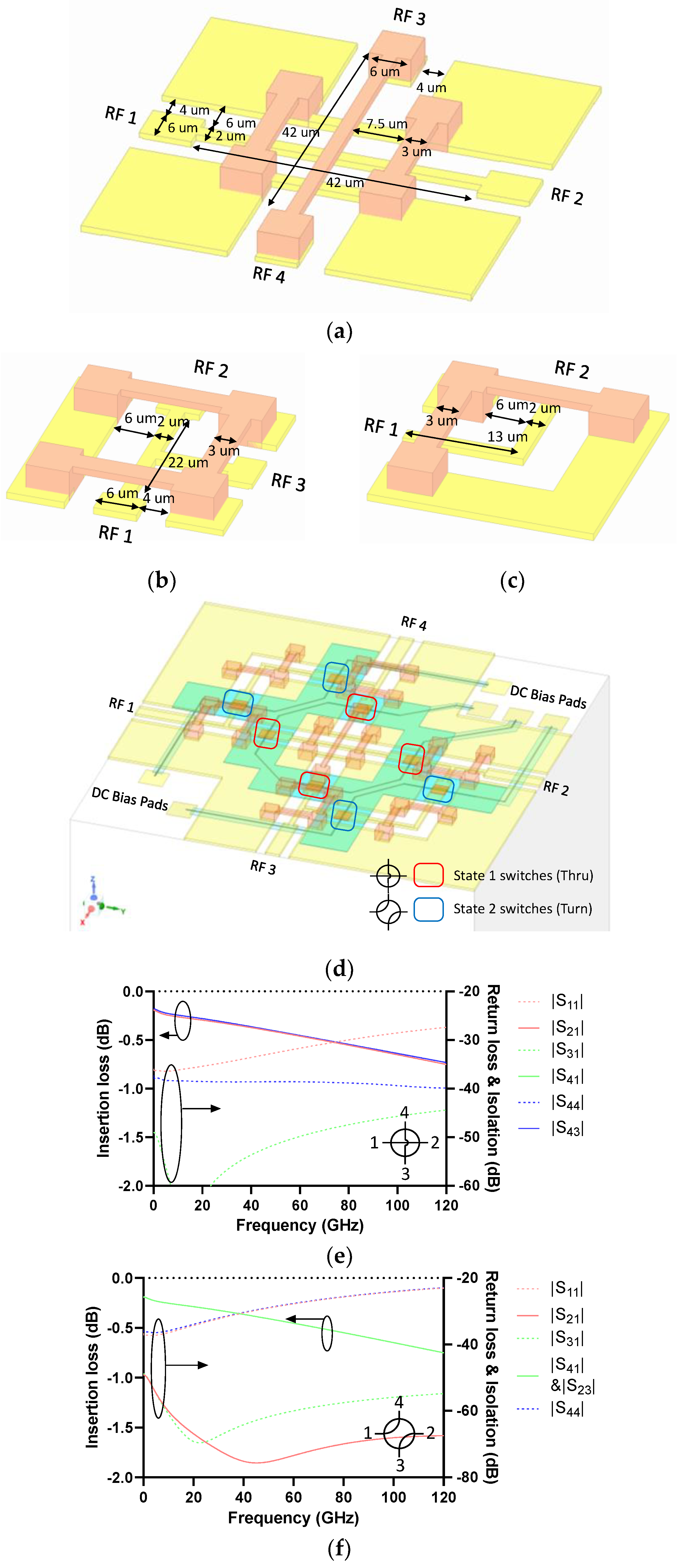
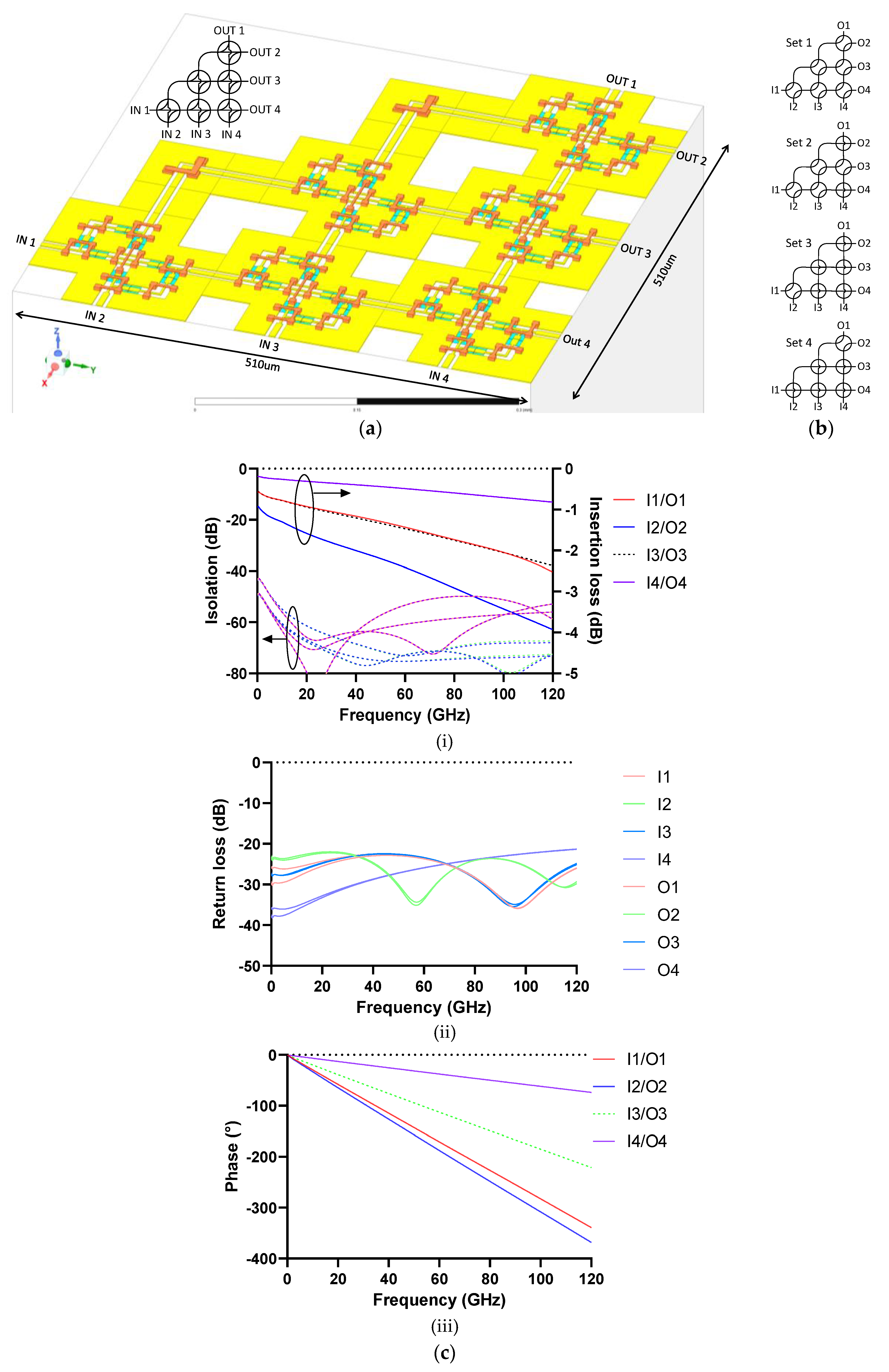
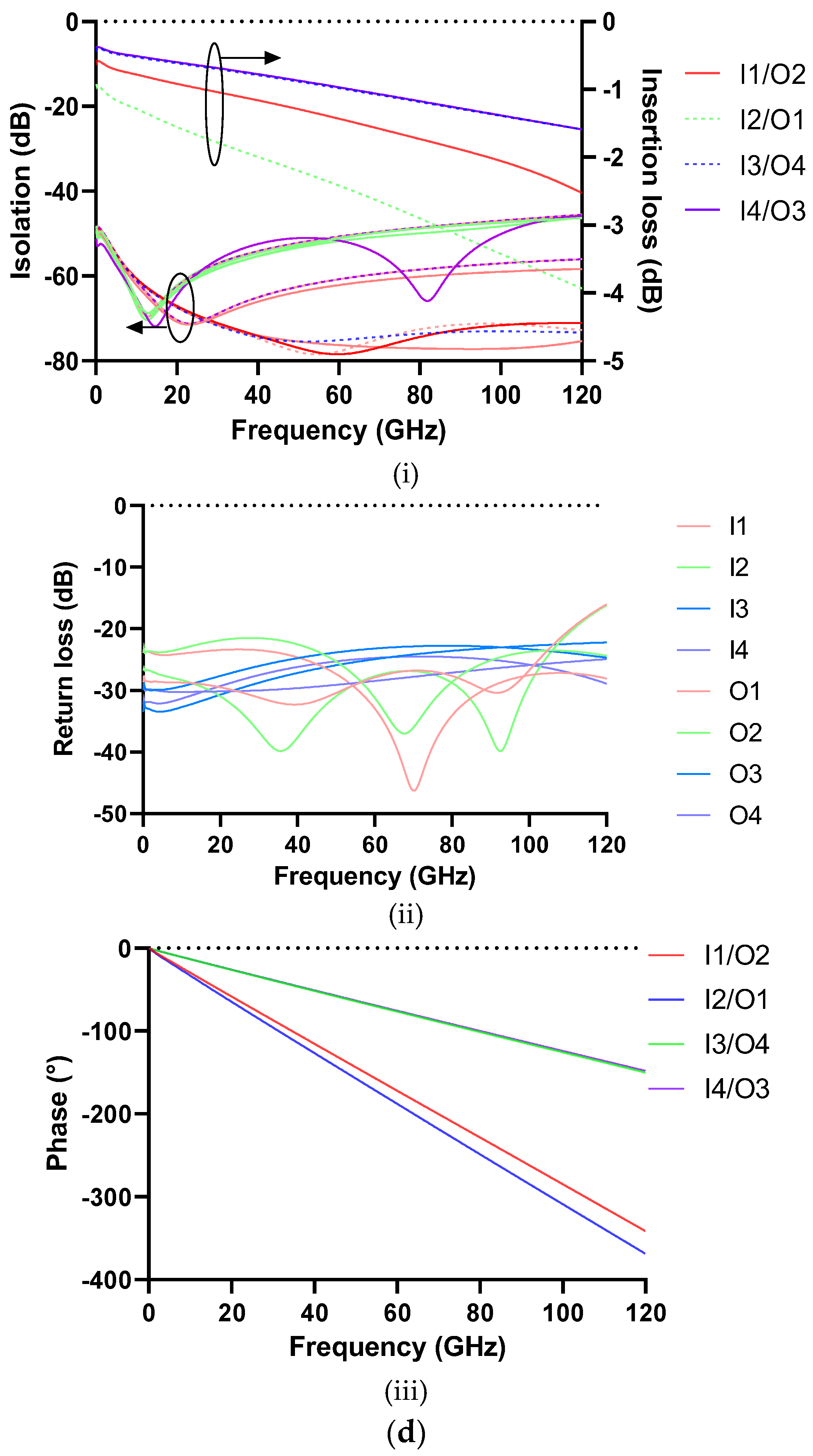
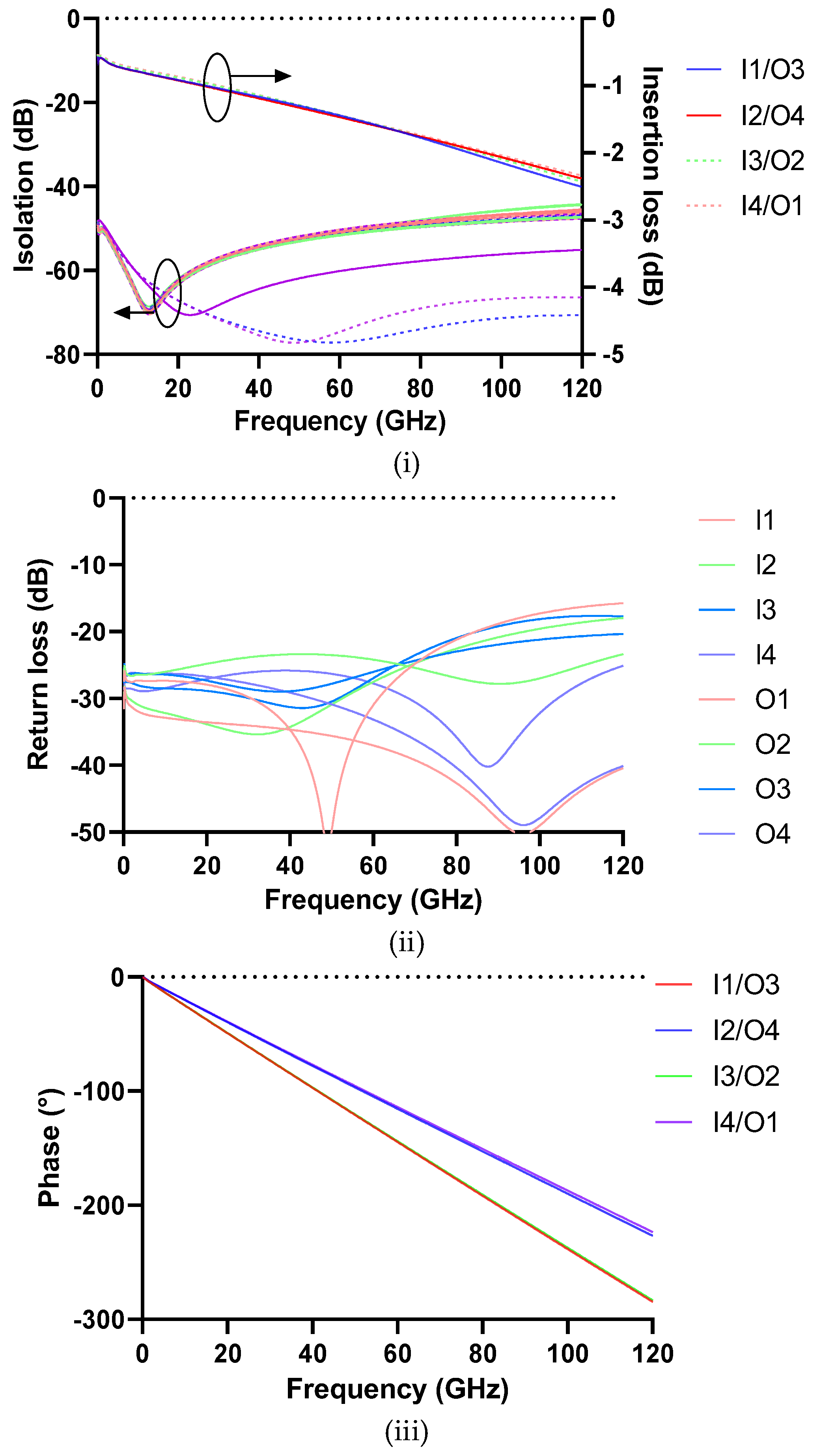
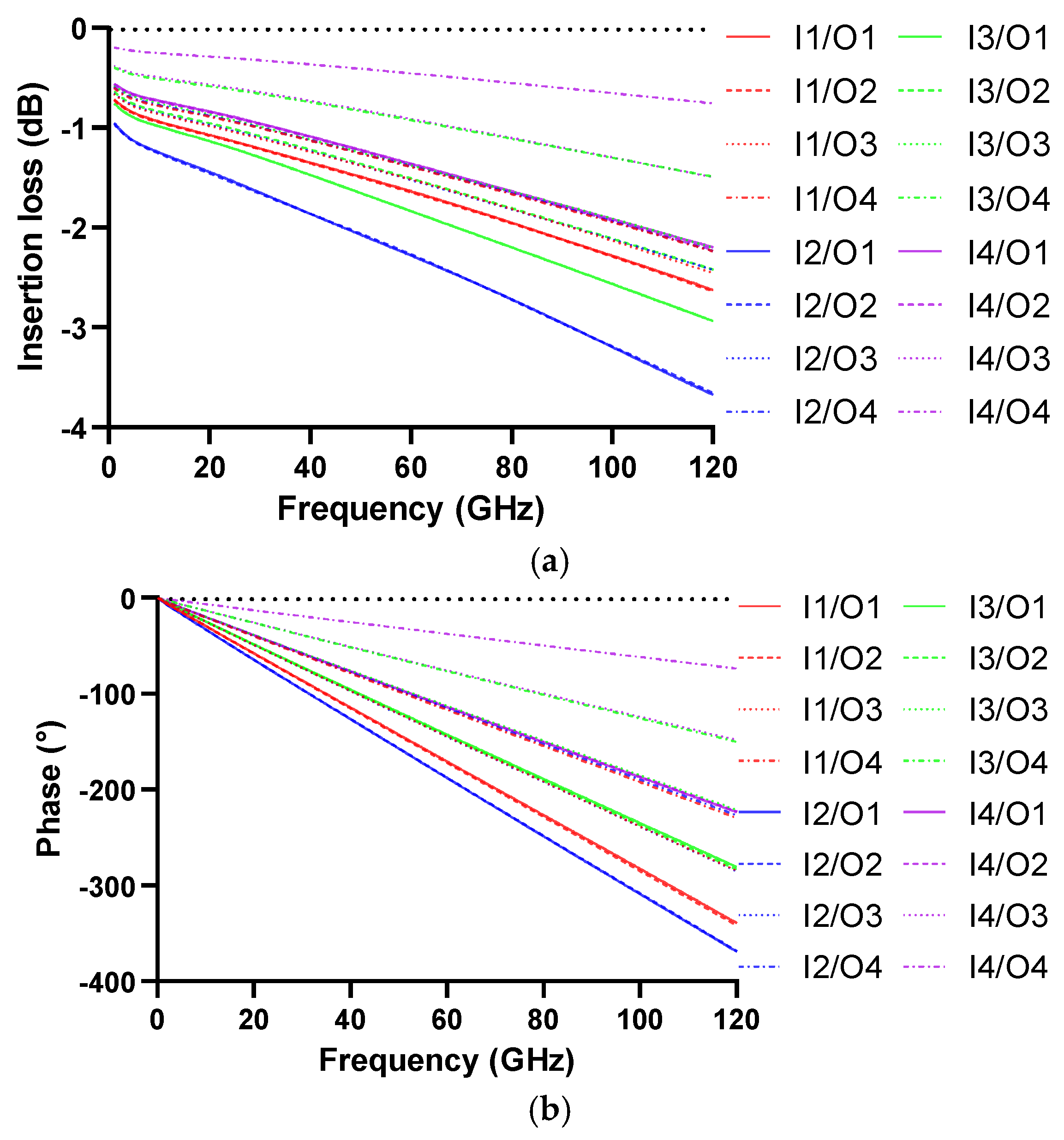
3. Design and Methodology
4. Conclusions
Author Contributions
Funding
Conflicts of Interest
References
- You, X.; Wang, C.-X.; Huang, J.; Gao, X.; Zhang, Z.; Wang, M.; Huang, Y.; Zhang, C.; Jiang, Y.; Wang, J.; et al. Towards 6G wireless communication networks: Vision, enabling technologies, and new paradigm shifts. Sci. China Inf. Sci. 2020, 64, 110301. [Google Scholar] [CrossRef]
- Campbell, C.F.; Dumka, D.C. Wideband High Power GaN on SiC SPDT Switch MMICs. In Proceedings of the 2010 IEEE/MTT-S International Microwave Symposium—IMS, Anaheim, CA, USA, 23–28 May 2010; pp. 145–148. [Google Scholar]
- Moon, J.S.; Seo, H.C.; Son, K.A.; Lee, K.; Zehnder, D.; Tai, H. 5 THz Figure-of- Merit Reliable Phase-change RF Switches for Millimeter-wave Applications. In Proceedings of the 2018 IEEE/MTT-S International Microwave Symposium—IMS, Philadelphia, PA, USA, 10–15 June 2018; pp. 836–838. [Google Scholar]
- Seki, T.; Yamamoto, J.; Murakami, A.; Yoshitake, N.; Hinuma, K.-I.; Fujiwara, T.; Sano, K.; Matsushita; Sato, F.; Oba, M. An RF MEMS switch for 4G Front-Ends. In Proceedings of the 2013 IEEE MTT-S International Microwave Symposium Digest (MTT), Seattle, WA, USA, 2–7 June 2013; pp. 1–3. [Google Scholar]
- Grant, P.D.; Denhoff, M.W.; Mansour, R.R. A Comparison between RF MEMS Switches and Semiconductor Switches. In Proceedings of the 2004 International Conference on MEMS, NANO and Smart Systems (ICMENS’04), Banff, AB, Canada, 25–27 August 2004; pp. 515–521. [Google Scholar]
- Rebeiz, G.M.; Patel, C.D.; Han, S.K.; Ko, C.H.; Ho, K.M.J. The Search for a Reliable MEMS Switch. IEEE Microw. Mag. 2013, 14, 57–67. [Google Scholar] [CrossRef]
- Wainstein, N.; Adam, G.; Yalon, E.; Kvatinsky, S. Radiofrequency Switches Based on Emerging Resistive Memory Technologies—A Survey. Proc. IEEE 2021, 109, 77–95. [Google Scholar] [CrossRef]
- Singh, T.; Mansour, R.R. Characterisation, Optimisation, and Fabrication of Phase Change Material Germanium Telluride Based Miniaturized DC–67 GHz RF Switches. IEEE Trans. Microw. Theory Tech. 2019, 67, 3237–3250. [Google Scholar] [CrossRef]
- Crunteanu, A.; Orlianges, J.C.; Bessaudou, A. Fast optical activation of insulator-to-metal transition in vanadium dioxide phase changed materials. Oxide-Based Mater. Devices 2020, 11281, 95–101. [Google Scholar]
- Leon-Valdes, J.; Huitema, L.; Arnaud, E.; Passerieux, D.; Crunteanu, A. Polarization Reconfiguration of a Millimeter-Waves Antenna using the Optical Control of Phase Change Materials. In Proceedings of the 2020 14th European Conference on Antennas and Propagation (EuCAP), Copenhagen, Denmark, 15–20 March 2020; pp. 1–4. [Google Scholar]
- El-Hinnawy, N.; Borodulin, P.; Wagner, B.P.; King, M.R.; Jones, E.B.; Howell, R.S.; Lee, M.J.; Young, R.M. Low-loss latching microwave switch using thermally pulsed non-volatile chalcogenide phase change materials. Appl. Phys. Lett. 2014, 105, 13501. [Google Scholar] [CrossRef] [Green Version]
- Chua, E.K.; Shi, L.P.; Zhao, R.; Lim, K.G.; Chong, T.C.; Schlesinger, T.E.; Bain, J.A. Low resistance, high dynamic range reconfigurable phase change switch for radio frequency applications. Appl. Phys. Lett. 2010, 97, 183506. [Google Scholar] [CrossRef]
- Wang, M.; Lin, F.; Rais-Zadeh, M. Need a Change? Try GeTe: A Reconfigurable Filter Using Germanium Telluride Phase Change RF Switches. IEEE Microw. Mag. 2016, 17, 70–79. [Google Scholar] [CrossRef]
- El-Hinnawy, N.; Borodulin, P.; Jones, E.B.; Wagner, B.P.; King, M.R.; Mason, J.S.; Bain, J.; Paramesh, J.; Schlesinger, T.E.; Howell, R.S.; et al. 12.5 THz Fco GeTe Inline Phase-Change Switch Technology for Reconfigurable RF and Switching Applications. In Proceedings of the 2014 IEEE Compound Semiconductor Integrated Circuit Symposium (CSICS), La Jolla, CA, USA, 19–22 October 2014; pp. 1–3. [Google Scholar]
- Moon, J.S.; Seo, H.C.; Le, D.; Fung, H.; Schmitz, A.; Oh, T.; Kim, S.; Son, K.A.; Yang, B. 10.6 THz figure-of-merit phase-change RF switches with embedded micro-heater. In Proceedings of the 2015 IEEE 15th Topical Meeting on Silicon Monolithic Integrated Circuits in RF Systems, San Diego, CA, USA, 26–28 January 2015; pp. 73–75. [Google Scholar]
- Slovin, G.; Xu, M.; Singh, R.; Schlesinger, T.E.; Paramesh, J.; Bain, J.A. Design Criteria in Sizing Phase-Change RF Switches. IEEE Trans. Microw. Theory Tech. 2017, 65, 4531–4540. [Google Scholar] [CrossRef]
- Singh, T.; Mansour, R.R. Investigation into Self Actuation Limitation and Current Carrying Capacity of Chalcogenide Phase Change GeTe-Based RF Switches. IEEE Trans. Electron Devices 2020, 67, 5717–5722. [Google Scholar] [CrossRef]
- Singh, T.; Mansour, R.R. Experimental Investigation of Performance, Reliability, and Cycle Endurance of Nonvolatile DC–67 GHz Phase-Change RF Switches. IEEE Trans. Microw. Theory Tech. 2021, 69, 4697–4710. [Google Scholar] [CrossRef]
- Singh, T.; Mansour, R.R. Ultra-Compact Phase-Change GeTe-Based Scalable mmWave Latching Crossbar Switch Matrices. IEEE Trans. Microw. Theory Tech. 2022, 70, 938–949. [Google Scholar] [CrossRef]
- Singh, T.; Mansour, R.R. Miniaturized DC–60 GHz RF PCM GeTe-Based Monolithically Integrated Redundancy Switch Matrix Using T-Type Switching Unit Cells. IEEE Trans. Microw. Theory Tech. 2019, 67, 5181–5190. [Google Scholar] [CrossRef]
- Singh, T.; Mansour, R.R. Scalable Non-Volatile Chalcogenide Phase Change GeTe-Based Monolithically Integrated mmWave Crossbar Switch Matrix. In Proceedings of the 2021 IEEE MTT-S International Microwave Symposium (IMS), Los Angeles, CA, USA, 7–25 June 2021; pp. 420–423. [Google Scholar]
- Singh, T.; Mansour, R.R. Monolithic PCM Based Miniaturized T-type RF Switch for Millimeter Wave Redundancy Switch Matrix Applications. In Proceedings of the 2019 IEEE MTT-S International Microwave Symposium (IMS), Boston, MA, USA, 2–7 June 2019; pp. 658–660. [Google Scholar]
- Singh, T.; Mansour, R.R. A Miniaturized Monolithic PCM Based Scalable Four-Port RF Switch Unit-Cell. In Proceedings of the 2019 49th European Microwave Conference (EuMC), Paris, France, 1–3 October 2019; pp. 180–183. [Google Scholar]
- Singh, T.; Mansour, R.R. Chalcogenide Phase Change Material GeTe Based Inline RF SPST Series and Shunt Switches. In Proceedings of the 2018 IEEE MTT-S International Microwave Workshop Series on Advanced Materials and Processes for RF and THz Applications (IMWS-AMP), Ann Arbor, MI, USA, 16–18 July 2018; pp. 1–3. [Google Scholar]
- Singh, T.; Mansour, R.R. Characterization of Phase Change Material Germanium Telluride for RF Switches. In Proceedings of the 2018 48th European Microwave Conference (EuMC), Madrid, Spain, 23–27 September 2018; pp. 475–478. [Google Scholar]
- Selimefendigil, F.; Öztop, H.F. Mixed convection in a PCM filled cavity under the influence of a rotating cylinder. Solar Energy 2020, 200, 61–75. [Google Scholar] [CrossRef]
- Hawasli, S.H.; Cruz, L.D.L.; El-Hinnawy, N.; Borodulin, P.; King, M.; Young, R.M.; Zaghloul, M.; Ivanov, T.G. Investigation of on-state power handling dependence on number of cycles for germanium telluride RF switches. In Proceedings of the 2017 IEEE MTT-S International Microwave Symposium (IMS), Honolulu, HI, USA, 4–9 June 2017; pp. 292–295. [Google Scholar]
- Cruz, L.D.L.; Birdwell, A.G.; Zaghloul, M.; Ivanov, T.G. GeTe Phase Change Research at the US Army Research Laboratory. In Proceedings of the 2018 IEEE/MTT-S International Microwave Symposium—IMS, Philadelphia, PA, USA, 10–15 June 2018; pp. 843–845. [Google Scholar]
- Moon, J.-s.; Seo, H.-c.; Son, K.-a.; Lee, K.; Zehnder, D.; Tai, H.; Le, D. Phase-change RF switches with robust switching cycle endurance. In Proceedings of the 2018 IEEE Radio and Wireless Symposium (RWS), Anaheim, CA, USA, 15–18 January 2018; pp. 231–233. [Google Scholar]
- Mennai, A.; Bessaudou, A.; Cosset, F.; Guines, C.; Passerieux, D.; Blondy, P.; Crunteanu, A. High Cut-off Frequency RF Switches integrating a Metal-Insulator Transition Material. In Proceedings of the IEEE MTT-S International Microwave Symposium, Phoenix, AZ, USA, 17 May 2015. [Google Scholar]
- Qiao, B.; Feng, J.; Lai, Y.; Cai, Y.; Lin, Y.; Tang, T.-a.; Cai, B.; Chen, B. Si–Sb–Te films for phase-change random access memory. Semicond. Sci. Technol. 2006, 21, 1073–1076. [Google Scholar] [CrossRef]
- Jeevan Fernandes, B.; Munga, P.; Ramesh, K.; Udayashankar, N.K. Electrical switching and thermal behavior of ternary Si15Te85-xBix (0 ≤ x ≤ 2) chalcogenide glasses. Mater. Today Proc. 2018, 5, 21292–21298. [Google Scholar] [CrossRef]
- Fernandes, B.J.; Ramesh, K.; Udayashankar, N.K. Electrical switching in Si20Te80−xBix (0 ≤ x ≤ 3) chalcogenide glassy alloys. J. Non-Cryst. Solids 2018, 483, 86–93. [Google Scholar] [CrossRef]
- Jagannatha, K.B.; Roy, D.; Das, C. Electrical switching and crystalline peak studies on Si20Te80−xSnx (1 ≤ x ≤ 7) chalcogenide bulk glasses. J. Non-Cryst. Solids 2020, 544, 120196. [Google Scholar] [CrossRef]
- Sharma, V.; Sharda, S.; Sharma, N.; Katyal, S.C.; Sharma, P. Chemical ordering and electronic properties of lone pair chalcogenide semiconductors. Prog. Solid State Chem. 2019, 54, 31–44. [Google Scholar] [CrossRef]
- Shaw, R.F.; Liang, W.Y.; Yoffe, A.D. Optical properties, photoconductivity, and energy levels in crystalline and amorphous arsenic triselenide. J. Non-Cryst. Solids 1970, 4, 29–42. [Google Scholar] [CrossRef]
- Kotkata, M.F.; Afifi, M.A.; Labib, H.H.; Hegab, N.A.; Abdel-Aziz, M.M. Memory switching in amorphous Ge∙Se∙Tl chalcogenide semiconductor films. Thin Solid Film 1994, 240, 143–146. [Google Scholar] [CrossRef]
- Li, X.; Chan, K.Y.; Ramer, R. E-Band RF MEMS Differential Reflection-Type Phase Shifter. IEEE Trans. Microw. Theory Tech. 2019, 67, 4700–4713. [Google Scholar] [CrossRef]
- Chan, K.Y.; Ramer, R.; Mansour, R.R. Novel Miniaturized RF MEMS Staircase Switch Matrix. IEEE Microw. Wirel. Compon. Lett. 2012, 22, 117–119. [Google Scholar] [CrossRef]
- Chan, K.Y.; Mansour, R.R.; Ramer, R. Miniaturized RF MEMS switch cells for crossbar switch matrices. In Proceedings of the 2010 Asia-Pacific Microwave Conference, Yokohama, Japan, 7–10 December 2010; pp. 1829–1832. [Google Scholar]
- Chan, K.Y.; Daneshmand, M.; Mansour, R.R.; Ramer, R. Scalable RF MEMS Switch Matrices: Methodology and Design. IEEE Trans. Microw. Theory Tech. 2009, 57, 1612–1621. [Google Scholar] [CrossRef]


| Material | On (Ωcm) | Off (Ωcm) | Off/On | Mechanism | ||
|---|---|---|---|---|---|---|
| GeTe | >170 | 735 | Heat | |||
| Ge2Sb2Te5 (GST) | 162–616 | 641 | Heat | |||
| Si10.7Sb39.5Te49.8 [31] | 2.5 | >200 | <600 | Heat | ||
| Si15Te85-xBix [32] | Heat | |||||
| Si20Te80-xBix [33] | Heat | |||||
| Si20Te80Snx [34] | 250 | Heat | ||||
| SeTe [35] | ~400 | Heat | ||||
| Se3Te [35] | ~400 | Heat | ||||
| As2Se3 [36] | Heat | |||||
| GeSeTl [37] | Heat |
Publisher’s Note: MDPI stays neutral with regard to jurisdictional claims in published maps and institutional affiliations. |
© 2022 by the authors. Licensee MDPI, Basel, Switzerland. This article is an open access article distributed under the terms and conditions of the Creative Commons Attribution (CC BY) license (https://creativecommons.org/licenses/by/4.0/).
Share and Cite
Ramer, R.; Chan, K.Y. Developing PCM-Based Microwave and Millimetre-Wave Switching Networks by Optimised Building Blocks. Electronics 2022, 11, 3683. https://doi.org/10.3390/electronics11223683
Ramer R, Chan KY. Developing PCM-Based Microwave and Millimetre-Wave Switching Networks by Optimised Building Blocks. Electronics. 2022; 11(22):3683. https://doi.org/10.3390/electronics11223683
Chicago/Turabian StyleRamer, Rodica, and King Yuk Chan. 2022. "Developing PCM-Based Microwave and Millimetre-Wave Switching Networks by Optimised Building Blocks" Electronics 11, no. 22: 3683. https://doi.org/10.3390/electronics11223683