Article

Design and Implementation of Scalable and Parametrizable Analog-to-Digital Converter on FPGA

by
Juan David Espitia Castillo
,
Enrique Cantó Navarro
and
Enric Vidal-Idiarte
*,†
Grup d’Automàtica i Electrònica Industrial (GAEI), Departament d’Enginyeria Electrònica Elèctrica i Automàtica, Campus Sescelades, Universitat Rovira I Virgili, Avinguda dels Països Catalans, 26, 43007 Tarragona, Spain
*
Author to whom correspondence should be addressed.
These authors contributed equally to this work.
Electronics 2022, 11(3), 447; https://doi.org/10.3390/electronics11030447
Submission received: 28 December 2021 / Revised: 29 January 2022 / Accepted: 30 January 2022 / Published: 2 February 2022

Abstract

:
The flexibility provided by FPGAs permits the implementation of several ADCs, each one configured with the required bit resolution and sampling frequency. The paper presents the design and implementation of scalable and parametrizable analog-to-digital converters (ADC), based on a successive approximation register (SAR), on FPGAs (field programmable gate arrays). Firstly, the work develops a systematic methodology for the implementation of a parametrizable SAR-based ADC from a set of building modules, such as the pulse-width modulator (PWM), external low-pass filter (LPF) and the analog comparator. The presented method allows choosing the LPF parameters for the required performance (resolution bits and sampling frequency) of a SAR-based ADC. Secondly, the paper also presents several optimizations on the PWM module to enhance the sampling frequency of implemented ADCs, and the method to choose the LPF parameters is adapted. The PWM and SAR logic are synthesizable and parametrizable, using a low number of resources, in order to be portable for low-cost FPGA families. The methodology and PWM optimizations are tested on a Zynq-7000 device from Xilinx; however, they can be adapted to any other FPGA.

1. Introduction

In the field of control systems, a set of signals are collected from sensors in order to perform the necessary actions to obtain the desired output from a reference indicated by the user [1,2]. A digital controller is usually implemented on a programmable device, such as a microcontroller, DSP, FPGA, etc. [3,4], which relies on ADCs to perform the required conversion of data acquired [5]. Important features of ADCs are the bit resolution (N), sampling frequency ( f S a m p l i n g ) and range of the input voltage ( V i n ).
There is a growing interest in MD (mostly digital) systems where most of the ADCs are implemented in the digital domain, simplifying its integration with digital cores (microprocessor, DSPs, Hw-accelerators, etc.) to build a SoC (system on a chip). The design flow provided by FPGA vendors allows the integration on embedded systems of digital circuits, such as FIR filters that might need external ADC [6]. Using discrete ADCs, such as LTC1406 (8-bit ADC 200 MSPS), in applications that require a high number of ADCs can inhibit its connection due the limited quantity of I/O pins in low-cost devices. In this case, a possible solution is to avoid the need for ADCs as shown in [7], where a digital signal is connected to a FPGA pin and its temporal width is measured by internal counters. Otherwise, FPGAs allow the implementation of ADCs, which, in the simplest case, requires a pin connected to a passive resistance-capacity (RC) filter and another pin to an internal logic gate acting as a analog comparator when the threshold voltage is exceed. However, the implementation of ADCs on FPGAs presents limitations, such as external analog circuits (integrators or filters), performance that cannot achieve discrete ADCs, and higher power consumption due to programmable technology.
Traditionally, digital controllers are implemented on microcontrollers or DSPs due to the development ease provided by programming languages and compiler [8,9]. However, the computing performance is limited by the sequential execution of instructions. FPGAs are programmable logic devices, which can implement a digital circuit using its hardware resources. The circuit is described in a hardware description language, typically Verilog or VHDL [10], and it is synthesized and implemented on the target device through automated design tools. Typically, the FPGA fabric is composed from a large set of logic resources, such as lookup tables (LUT) [11], flip-flops (FF), input–output blocks (IOBs) and others, that are interconnected through configurable routing resources. The available hardware resources allow the implementation of highly parallel circuits for multiple controllers that can greatly accelerate computations on FPGAs compared to a microcontroller or DSP.
An application such as SDR (software-defined radio) needs ADCs with high f S a m p l i n g on the IF (intermediate frequency) stages to enable the digital sample processing. Most advanced SDRs are able to remove conversion stages to IF, reducing operational amplifiers, filters and other analog elements, using high-performance ADCs (GSPS). The high-performance ADCs are usually implemented on full-custom integrated circuits and use time-interleaving techniques that require several ADCs in parallel to convert the same input [12,13,14,15].
ADCs are not usually integrated on low-cost FPGAs. Some high-performance FPGAs may integrate an ADC, which can be insufficient for multiple controllers converting simultaneously several signals at different sampling frequencies, resolutions and voltage ranges. For example, in on-board battery charges for electrical vehicle, working in one or three phases, a large amount of signals need to be read for control and protection purposes [16,17,18]. In [19,20], reading several signals is needed to control simultaneously multiple independent power converters by a single DSP, where the processor is implemented on a FPGA. In biomedical applications, multi-channel acquisition are simultaneously needed [21], while in battery management systems, several signals are used at the same time for monitoring and protection purposes [22]. In such cases, external ADCs can be attached to the FPGA at the expense of additional cost.
The paper proposes a methodology to implement scalable and parametrizable ADCs on FPGAs. The scalability permits the implementation of several ADCs on a single FPGA device, each one configured according to a set of parameters to individually adjust the required sampling features (N, f S a m p l i n g ). The ADC architecture is based on a SAR controlling a DAC (digital-to-analog converter), which is built using a PWM and external LPFs. The SAR and PWM circuits can be implemented in the LUTs and FFs available in almost any FPGA family. The circuits do not rely on special hardware resources for a particular device (delays on carry chain), external input, such as space vector PWM [23], sinusoidal PWM [24], or carrier phase shifted PWM [25] used in other applications or specific tools from a device vendor that would limit the porting to different FPGA families. Moreover, the presented work also describes several optimizations of the PWM devoted to increase the maximum selectable f S a m p l i n g .
Section 2 presents the state of the art where recent works related to fully synthesizable ADCs, ADC fully implemented on FPGAs, and SAR-based ADCs, among others, are shown. Section 3 introduces the SAR-based ADC, focusing on the analysis of the PWM module and the attached low-pass filter (LPF) that built the DAC. It finally presents a methodology to design a parametrizable ADC. Section 4, Section 5 and Section 6 present and analyze three optimizations devoted on improving the f S a m p l i n g : double data rate PWM, paralleled PWM, and distributed duty-cycle PWM. The next section analyzes the combination of the three optimizations. The experimental results are reported in Section 8. Section 9 and Section 10 present the discussion and conclusions, respectively.

2. State of the Art

Flash-type ADCs are based on a large set of analog comparators and a priority encoder. Each comparator generates a digital channel from comparing V i n against a scaled voltage from V R E F . Although they provide high conversion rates, the power consumption, implementation area and linearity errors are important issues. Stochastic flash ADCs improve the linearization of the conversion by further increasing the number of comparators and adding an interpolation circuit at each digital channel. They are mixed-signal circuits that are usually implemented on custom CMOS integrated circuits [26] (8190 comparators, 6.2 ENOB, 100 MSPS) or synthesized on standard cells [27] (2040 comparators, 5.2 ENOB, 320 MSPS), [28] (2047 comparators, 5.7 ENOB, 210 MSPS). Nevertheless, flash ADCs are not suitable on FPGAs due to the large number of required external comparators and I/O connections. VCO-based ADCs can achieve a high sampling frequency. They are composed of an oscillator, a quantizer and a differential module. The works [29,30] showed a VCO-based ADC, which is fully synthesizable and described using a digital HDL, implemented in standard cell 65 nm CMOS. An architecture to eliminate the non-idealities of the coarse and fine VCO-based quantizers by replacing them with a PWM and filters is presented in [31]. The described VCO-based ADCs are implemented in CMOS technology and require a significant amount of I/O connections and methods to improve linearization. A sigma-delta ADC presented in [32] is implemented with simple analog circuit on a FPGA Virtex-4, using differential input, and requiring more complex digital circuitry. A high precision and low sampling frequency sigma-delta-based ADC on a A3PE3000 flash FPGA is used in [33] to balance a dynamically tuned gyroscope. Using the low voltage differential signal (LVDS) receiver inside the FPGA and an integrator, ref. [34] implemented a sigma-delta ADC for a current sensing application.
Most of the high-performance ADCs in FPGAs are based on a time-to-digital converter (TDC) architecture [35,36,37]. They are based on the temporal measurement of charging a RC circuit until V i n is reached. A comparator generates a digital pulse proportional to V i n , and the TDC circuit measures the width of this pulse. Although the TDC circuit can be easily implemented by a digital counter, these implementations greatly improve the f S a m p l i n g by a delay network. The delay network is composed of a large number of sections of a specific FPGA resource devoted to transmitting the input to the output with a known delay by estimation or measurement. The conversion code is generated from the large number of signals retrieved from the delay network. The precision stability of TDC-based ADCs is greatly affected by the tolerances of R and C values, and by temperature or voltage fluctuations. Therefore, they usually require periodic calibration.
The 600 MSPS 7-bit ENOB (effective number of bits) ADC presented in [38] is a high-speed converter implemented in an UltraScale+ FPGA from Xilinx, with a periodic calibration circuit. The ADC implements a tapped-delay line, an edge detection circuit attached to an encoder to generate the conversion result, and a periodic calibration circuit. In this particular case, the delay is measured through a tapped-delay line, which is composed of 426 multiplexor-XOR sets from the UltraScale+ carry logic. The ADC does not require external components, since an output buffer (OBUF) and a differential input buffer (DIFFINBUF) from UltraScale+ replace the capacitor, resistance and the analog comparator. Xilinx allows configuring the slew rate and the desired impedance of the OBUF, which is externally connected to a DIFFINBUF that provides a parasitic capacitance. The DIFFINBUF is used as an analog comparator, connecting one input to the OBUF and the other to V i n , generating a digital output when the input difference crosses the threshold voltage. Nevertheless, the tolerance on the CMOS manufacturing process of integrated circuits can significantly affect the electrical values, such as the parasitic capacitance and the threshold voltage of the DIFFINBUF and the transistor impedance of the OBUF. Moreover, the non-linear relationship between V i n and time requires a higher number of signals retrieved from the delay line and its encoder, which requires periodic calibration to maintain the precision stability due to variations.
The 200 MSPS, 6-bit ENOB ADC presented in [35] is a bit simpler. It implements a tapped-delay line but is based only on the multiplexors of the carry chain from Spartan-6 FPGA. Moreover, this ADC requires an external resistance to charge the parasitic capacitance from a DIFFINBUF. Another example is the 100 MSPS 6-bit (3.8 ENOB) ADC presented in [36], which must be maintained in cryogenic temperatures by a liquid helium environment at 4 °K. It also uses a DIFFINBUF attached to an external resistance, although it uses ISERDES (input serializer/deserializer) from Artix-7 to implement the tapped-delay line.
Using very specific hardware resources from a FPGA device to implement ADCs makes portability to other families very difficult. The hardware resources that implement the tapped-delay line cannot be placed and routed by automated tools, as they must be manually located and interconnected in the FPGA to achieve the desired delays. Moreover, the differences in the electric parameters between FPGA families may require redesigning the encoder and delay line. Finally, these ADC are designed and tested for specific ADC requirements, meaning they are not parametrizable to other resolution bits and sampling rates. Changing these requirements makes it necessary to change the delay line, calculate or measure the new propagation times and the encoder tuning.
The ADC proposed in this work is a SAR-based ADCs. Although SAR-based ADCs cannot reach the f S a m p l i n g of TDC-based ADCs, they can provide several advantages, such as portability to other FPGAs and adaptability to different ADC requirements. The ADC is composed of a SAR, a DAC (digital PWM and an external filter) and analog comparator. The PWM and filter is the most economic option to implement the DAC, as described in [39], and the external components, such as resistance and capacitors are chosen with 1% tolerance to avoid periodical calibration. The SAR and PWM circuits are described in portable VHDL descriptions since the synthesized result only requires the flip-flops and look-up tables available on any FPGA. The circuits are also parametrizable to the ADC requirements ( f S a m p l i n g and resolution bits), and scalable allowing to implement several ADCs on a device due to the low number of devoted resources. Moreover, depending on the ADC requirements, several PWM optimizations can be applied to improve f S a m p l i n g .
The SAR-based ADC presented in [40] is a more similar solution to the proposed one. The converter is built from an internal DAC [39,41,42], composed of a Dyadic PWM and a passive RC filter, which is fully-synthesizable on standard cell 40 nm CMOS technology. However, this solution uses instances to the library of the CMOS technology in order to permit the filter implementation by using the automatic translation tools. This way, the R of the filter is implemented on the high-resistivity polysilicon layer, and the C by using the metal–insulation–metal capacitance provided in the 6th metal layer of the target technology. Obviously, these type of instances are not available in FPGA libraries, and the filter must be externally implemented, as in our case. The ADC performance is very limited, providing f S a m p l i n g = 2.8 kSPS and 7-bit resolution (6.4 ENOB). Compared to other ADCs—completely or partially synthesizable on a standard cell, with flash architecture, sigma-delta or based on a VCO—its main advantage is the important reduction of the implementation area and power consumption and being fully synthesizable for an easy integration.
A very recent SAR-based ADC is presented in [43], which improves the previous ADC, achieving 10 MSPS and 7.5 ENOB. The ADC is synthesizable in standard cell 65-nm CMOS technology, and it is based on an inverter-based RDAC (Resistive DAC), a compensating LUT and a OAI-based (or-and-inverter) comparator. The OAI-based comparator replaces the single logic gate used as an analog comparator, allowing the OR to reset the transistor nodes of the AND preamplifier in order, eliminating residue charges at nodes that undermine ADC linearity. The inverter-based RDAC permits to eliminate the LPF, reducing the t S e t t l i n g to enhance the f S a m p l i n g , but increases the I/O connectivity and requires compensation circuitry due to the non-linear resistance offered by the transistors from inverters. The compensating LUT is tuned according to the simulation results to independently switch on/off inverters of the RDAC, improving conversion linearity. Implementing an internal RDAC in FPGAs is not possible, as they do not provide internal resistors, except for pull-up/pull-down transistor-based impedance available only at I/O blocks. The inverter-based RDAC would be theoretically possible, but the resistance values are very dependent on the FPGA family, as in the tapped-delay line, and consequently, this approach would not be easily portable or parametrizable.

3. SAR-Based ADC

A SAR-based ADC compares the voltage at its input ( V i n ) with a continuous voltage generated by a DAC ( V D A C ) from the binary number (B) driven by the SAR. The ADC evaluates a set of voltage levels converging to input voltage after several iterations [44,45]. Starting from the MSB (most significant bit) of the result, it computes a new bit by comparing the V D A C with the V i n at each iteration, increasing or decreasing the V D A C to converge to the input voltage V i n [46].
At the start of the conversion, the SAR initializes the MSB of the conversion result (B) to ‘1’ and the rest of the bits to ‘0’. The SAR output attaches to the DAC to generate the V D A C , which is compared with V i n . During each iteration, the SAR writes the currently evaluated bit of B by reading the comparator output V C o m p a r a t o r , generating a new V D A C for the next iteration. If V C o m p a r a t o r equals to ‘1’, this means the V D A C voltage is lower than V i n , and, consequently, the current bit is written to ‘1’. Otherwise, the SAR stores ‘0’ in the evaluated bit since the V D A C is higher than V i n . Then, the following bit of B is initialized to ‘1’ in order to generate the V D A C for the next iteration, as depicted in Figure 1. In an N-bit ADC, the process finishes when the LSB (least significant bit) is evaluated, after N iterations, obtaining the value of B that represents V i n .
Each bit requires a settling time ( t S e t t l i n g ) due to the analog components involved in the DAC and the comparator. Therefore, in a N-bit ADC, the frequency sampling is computed as
f S a m p l i n g = 1 N · t S e t t l i n g

3.1. DAC Implementation with PWM and LPF

The ADC replaces a resistor ladder DAC architecture with a PWM [47], which is implemented in the FPGA, and an external LPF, as shown in Figure 2. The output voltage of the LPF ( V L P F ) is proportional to the duty cycle (D) of the PWM. The range of D is 0 D < 1 according to Equation (2), where d denotes the value at the PWM input. Finally, the V L P F voltage is shifted 1 2 L S B to generate the V D A C required by the analog comparator, according to Equation (3). An analog adder performs the voltage shifting in order to reduce the ADC offset error from ±LSB to ± 1 2 LSB.
D = d 2 N 0 d 2 N 1
V D A C = V L P F L S B 2
The allowed range of voltages at the input V i n of the ADC is related to the output voltages at the FPGA ports. V O H and V O L denote the output voltages at a FPGA port driving the logic levels ‘1’ and ‘0’, respectively. The V L P F is obtained according the Equation (4), where the average voltage ( V L P F ¯ ) is related to D and Δ V O = V O H V O L . However, the V L P F also carries a sinusoidal wave Δ V L P F ( t ) due to the limited attenuation of the LPF. The peak-to-peak voltage of Δ V L P F ( t ) , denoted as Δ V L P F , depends on the the cutoff frequency ( f C ) and order ( O L P F ) of the filter and must be lower than the ADC analog resolution ( L S B ), as expressed in Equation (5).
V L P F ( t ) = V L P F ¯ + Δ V L P F ( t ) V L P F ¯ = D · Δ V O
Δ V L P F < L S B L S B = Δ V O 2 N

3.1.1. PWM Module

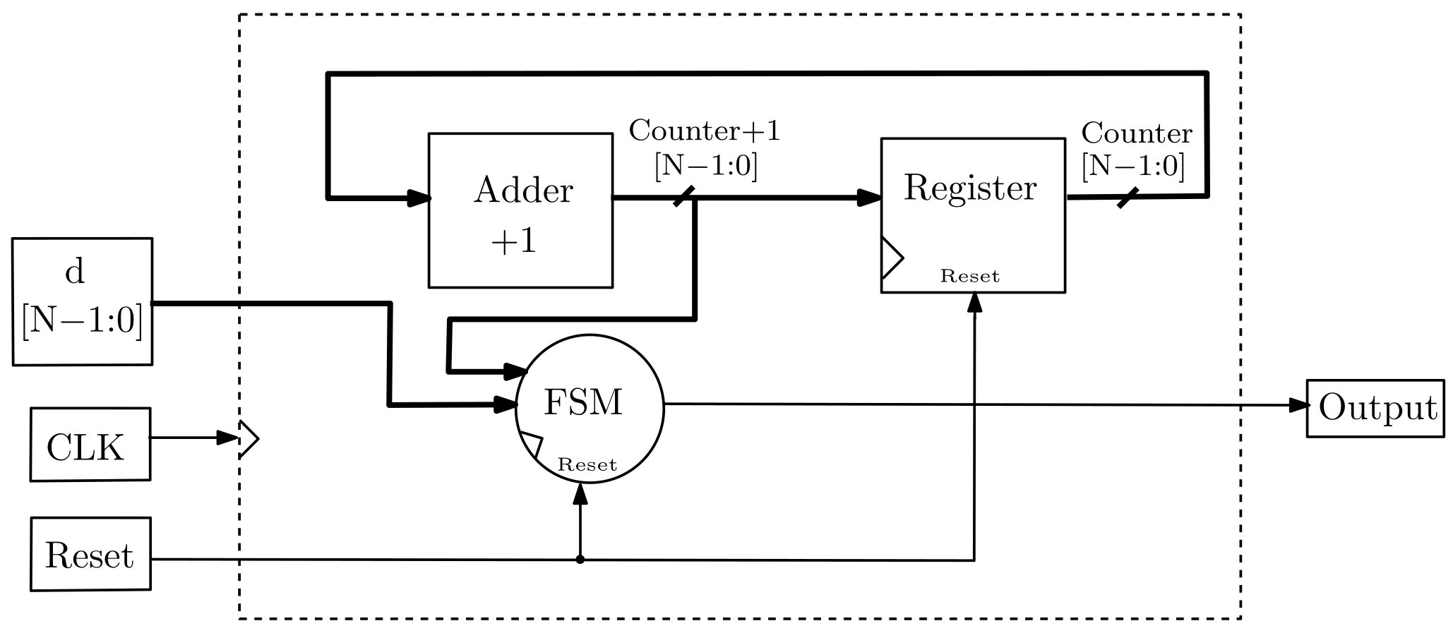
The PWM schematic is presented in Figure 3. The PWM module is implemented on the FPGA by an ascending N-bit counter and a FSM (finite state machine). Each PWM period is composed of 2 N counts, from 0 to 2 N 1 , by incrementing the counter register at each rising edge of the input clock. Therefore, the PWM frequency f P W M is obtained according to Equation (6), where f c l k denotes the clock frequency of the FPGA.
f P W M = f c l k 2 N
The FSM state changes when the counter is restarted to 0 or when it is going to achieve the input d, asserting or deasserting the PWM output, respectively. The duty cycle at the PWM output is D = d 2 N , where the range of the digital input d is from 0 to 2 N 1 .
Fourier transform is applied in order to analyze the Δ V L P F from the filtered PWM output. The PWM output is a square waveform characterized by the duty cycle D, and its transform is composed of the continuous coefficient A 0 and the set of harmonic coefficients A n and B n [48,49], as shown in Equation (7).
A 0 = D · Δ V O = d 2 N · Δ V O B n = 0 A n = 2 · Δ V O n π sin n π D
The A n harmonics depends on D. The first harmonic A 1 is the most significant coefficient affecting Δ V L P F [50], which is maximal when D = 1 2 [51], as expressed in Equation (8).
A 1 ( m a x ) = 2 · Δ V O π sin π 2 = 2 · Δ V O π
The maximum peak-to-peak voltage ripple at the LPF output is mainly obtained from filtering the first harmonic of the PWM, as shown in Equation (9).
Δ V L P F = A L P F ( f P W M ) · 4 ( Δ V O π )
A L P F ( f P W M ) represents the filter magnitude gain at the PWM frequency. Therefore, from Equations (5) and (9), it can be obtained an upper limit for the LPF magnitude gain at f P W M , as in Equation (10).
A L P F ( f P W M ) < π 4 · 1 2 N

3.1.2. Low-Pass Filter (LPF)

In order to avoid an ADC conversion error due to the LPF, Equation (10) must be satisfied to ensure the Δ V L P F at the LPF output is lower than the ADC analog resolution. Since the f P W M is constant, the f C and O L P F of the filter are calculated to properly reduce the Δ V L P F . Reducing f C can achieve the goal, because Δ V L P F is proportional to the f C / f P W M ratio. Furthermore, increasing the filter order O L P F also reduces Δ V L P F since the asymptotic attenuation slope of the LPF is O L P F · 20 d B d e c at filtered frequencies. However, both solutions also increase t S e t t l i n g .
The LPF implemented is a Bessel filter, as it has the shortest settling time ( t S e t t l i n g ) compared to other types of filters [52]. A lower t S e t t l i n g reduces the conversion time, enhancing the ADC sampling frequency ( f S a m p l i n g ). The Bessel LPF is implemented on a Sallen–Key topology. A Sallen–Key stage implements an O L P F = 2 filter by a pair of resistors and capacitors attached to an operational amplifier (OA). Several stages are cascaded to increment the O L P F .
It is required to find a trade-off solution for the LPF. The t S e t t l i n g is noticeably much more affected by decreasing f C than by increasing the O L P F . A solution based exclusively on incrementing O L P F requires more stages and circuit complexity, but a solution solely based on reducing the f C significantly affects the t S e t t l i n g .

3.1.3. LPF Parameters for a N-Bit SAR-Based ADC

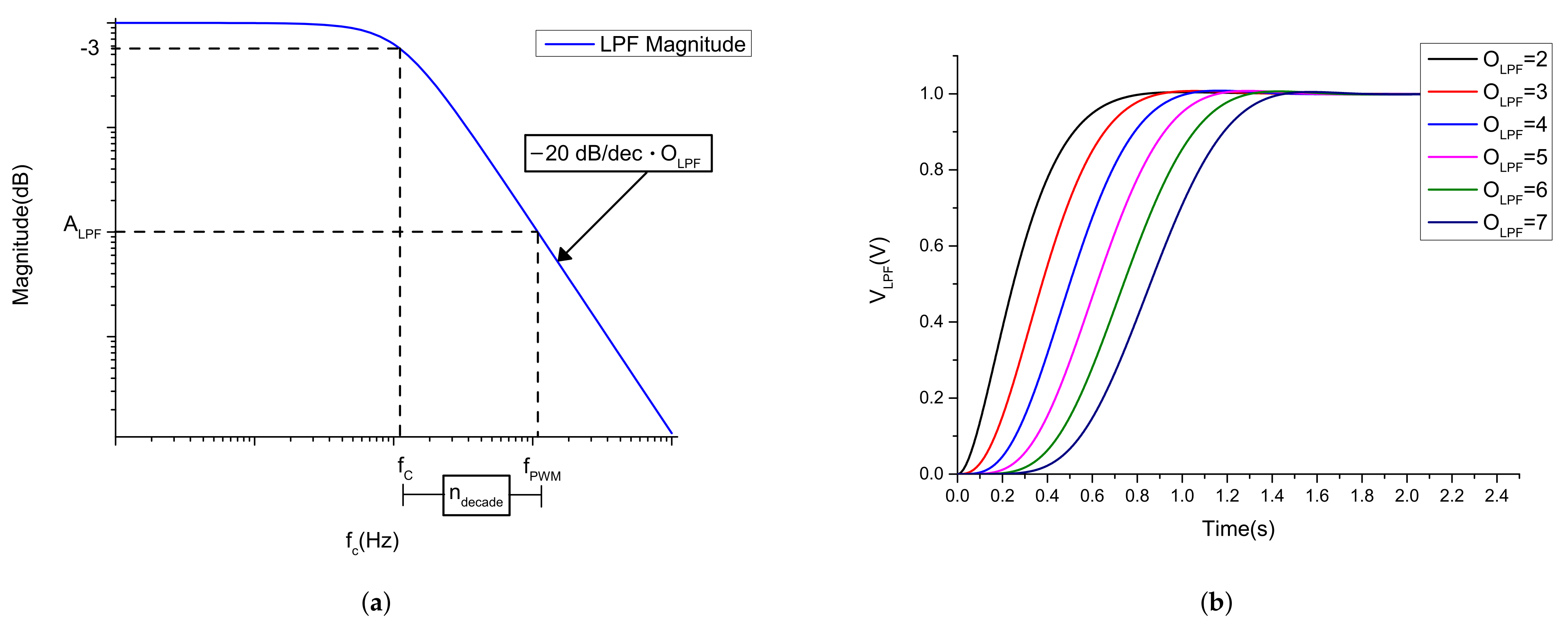
It is presented a methodology to obtain the optimal LPF parameters ( f C and O L P F ) from the ADC resolution (N) and the required f S a m p l i n g . The magnitude plot of the frequency response of a Bessel LPF, according to f C and O L P F , is depicted in Figure 4a, and Figure 4b shows the normalized step response of the Bessel LPF for different O L P F .
Firstly, Equation (11) computes the maximum filtered PWM output from Equation (10) in logarithmic scale. The filtered PWM output at f P W M is shown in Equation (12).
A L P F ( m a x ) = 20 · log 10 π 4 · 1 2 N
A L P F ( f P W M ) = 20 · O L P F · log 10 f P W M f C = 20 · O L P F · log 10 f c l k 2 N · f C
Since the condition A L P F ( f P W M ) < A L P F ( m a x ) must be accomplished, Equation (13) is obtained from the previous two equations, which is applied to calculate a set of maximum cutoff frequency f C and filter order O L P F pairs that satisfy the required attenuation. The selected solution is the pair with the minimal O L P F that accomplishes the required f S a m p l i n g , as expressed in Equation (14)
O L P F · log 10 f c l k 2 N · f C < log 10 π 4 · 1 2 N f C f c l k < π O L P F 2 2 + N + N · O L P F O L P F
1 N · t S e t t l i n g f S a m p l i n g

3.1.4. FPGA Implementation of an 8-Bit SAR-Based ADC

The FPGA used to test the implementation of a 8-bit SAR-based ADC is from the Zynq-7000 Xilinx family. The clock frequency is f c l k = 100 MHz and the input/output blocks are configured to Δ V O = 3.3 V. However, the settings can be changed for others FPGAs following the same methodology. The design parameters are shown in Table 1.
Following the steps described in Section 3.1.3, it is calculated the set of solutions ( f C , O L P F pairs) shown in Table 2. The adopted solution should be based on the required f S a m p l i n g for the specific application. The t S e t t l i n g is obtained from normalized LPF step response presented on Figure 4b for the different O L P F .
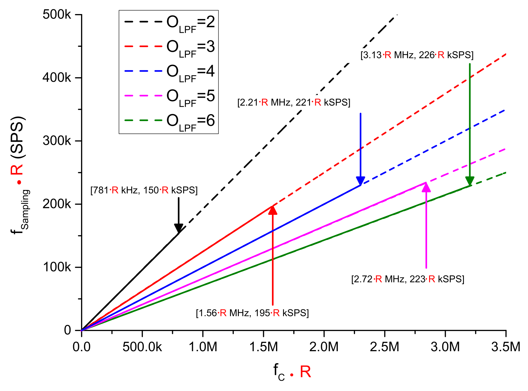
Figure 5 shows graphically the allowed solutions of f C vs. f S a m p l i n g for different O L P F in the 8-bit ADC. Valid solutions are below the maximum cutoff frequency, and solutions that do not accomplish the required attenuation are represented by dashed lines. The values of f S a m p l i n g and f C are normalized at f c l k = 100 MHz, and, consequently, they can be easily calculated for other clock frequencies by simple multiplication with a ratio R, represented in Equation (15).
R = f c l k 100 MHz
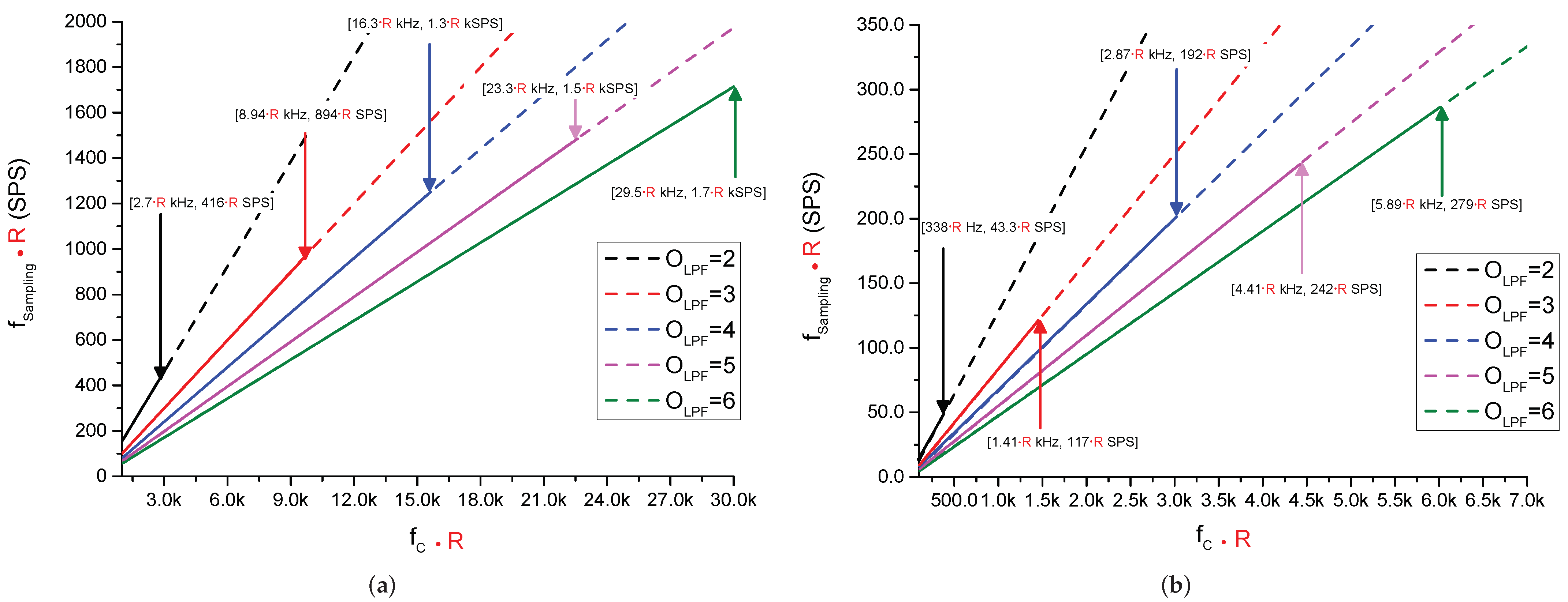
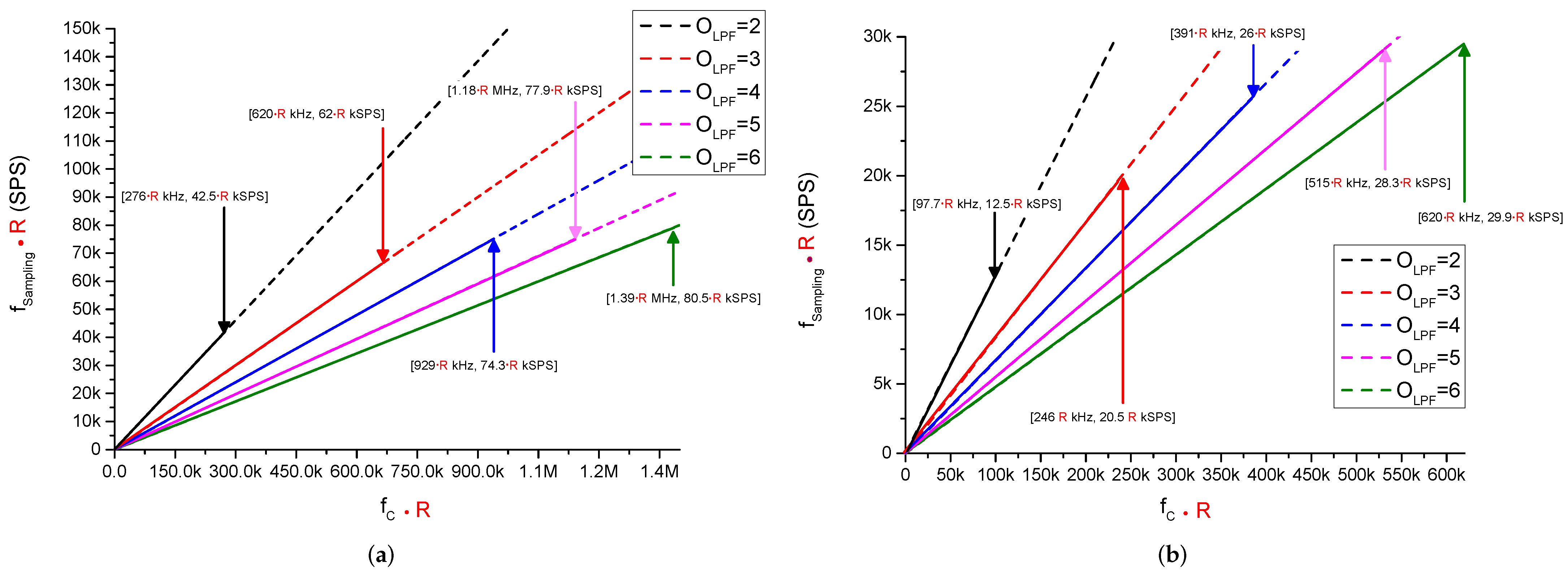
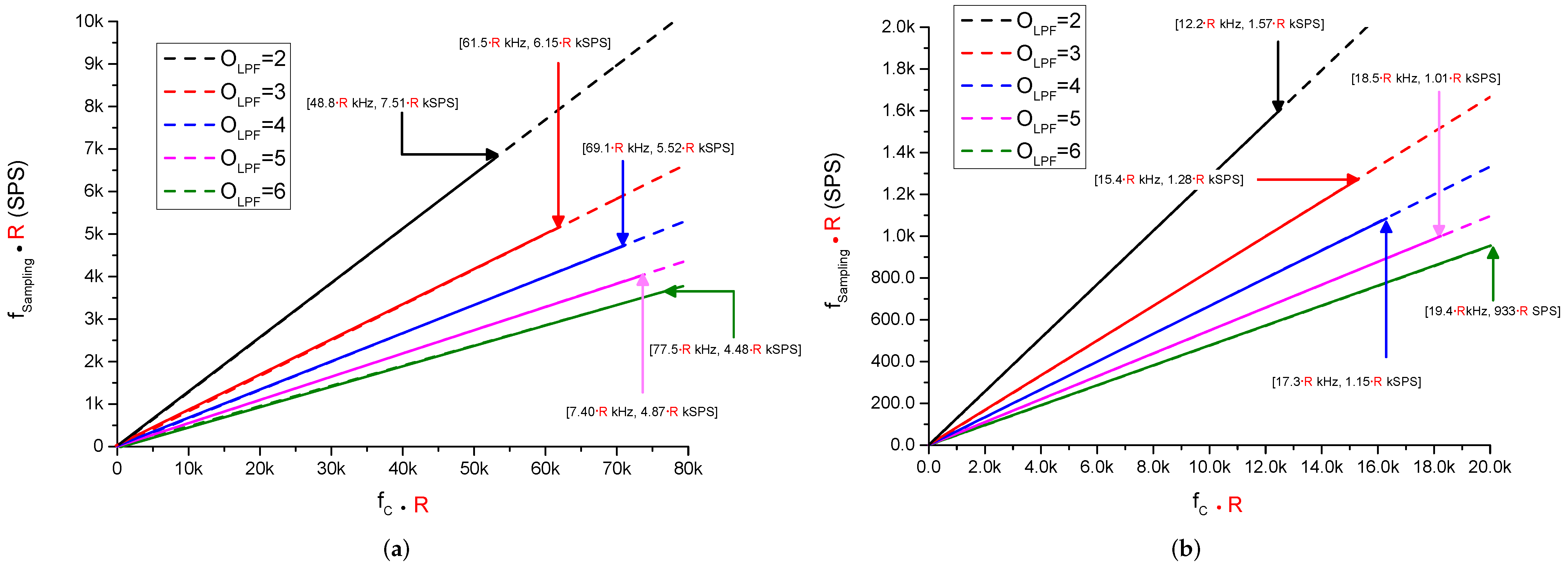
The same procedure is used for an N-bit ADC. Figure 6a,b shows f C vs. f S a m p l i n g for 10-bit and 12-bit ADCs, respectively.
Figure 7 shows the simulation model of the ADC in Simulink-Matlab and the System Generator tool from Xilinx. The Xilinx tool permits simulation of VHDL hardware descriptions attached to circuit models, such as the Bessel LPF, the analog adder and comparator. Firstly, we provide to the VHDL modules the number of bits (N) and t S e t t l i n g of the LPF, in order to configure the ADC controller which drives the SAR. N also configures the SAR and PWM modules. The controller periodically starts ADC conversions, initializing the SAR register. It also asserts the bit-acquisition signal when the t S e t t l i n g is achieved, in order to store the comparator result into the current converted bit of the SAR and storing a ‘1’ to the next conversion bit. The SAR stores the d value, which drives the PWM input in order to generate the corresponding modulated output. The filter gets V L P F from the modulated signal, in order to obtain its averaged value, which is shifted 1 2 L S B by the analog adder to V D A C and compared with the V i n . After N iterations, the SAR stores the last d value into a register to provide the conversion result (B).
Figure 8 shows the simulation result for the 8-bit ADC with O L P F = 6 and f C = 148.9 kHz solution. We can observe that V D A C starts at the voltage Δ V o 2 and converges to V i n after eight iterations, each one requiring t S e t t l i n g = 1.75 μ s. The signals driven by the ADC controller start the conversion and the bit change in the SAR.
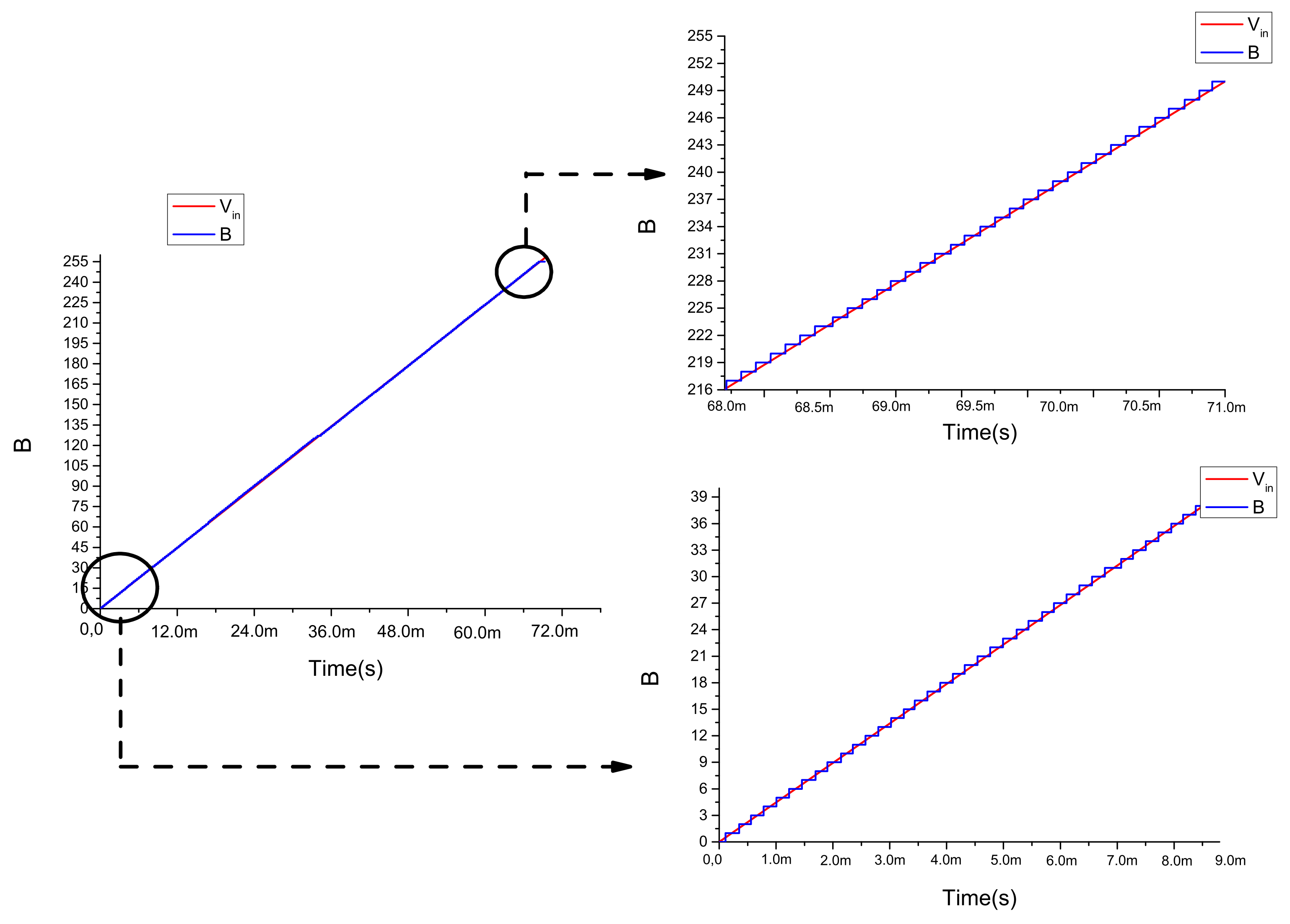
Finally, Figure 9 depicts the conversion results, where we can see B is correctly obtained for a voltage ramp V i n from V O L to V O H .

4. Double Data Rate PWM

Double date rate (DDR) registers in FPGAs are usually devoted as interface logic attached to external synchronous dynamic RAM memories, although other applications can use them to double the acquisition rate [53]. Therefore, DDR registers are not available in the internal FPGA fabric, but they are located in the input/output blocks [54,55]. An output DDR (ODDR) flip-flop can drive its output with two different logic levels during a single clock cycle, one logic level synchronized at the rising edge of the clock and the other level at the falling edge.
An easy way to increment f S a m p l i n g is by using the input clock as the least significant bit of the the internal PWM counter and driving the FSM output through an ODDR flip-flop, doubling the f P W M from Equation (6), as expressed in Equation (16).
f P W M D D R = 2 · f c l k 2 N = 2 · f P W M
Therefore, Equation (13) is modified since f P W M in Equation (10) is increased due to the DDR register, obtaining the solutions f C and O L P F of the filter in the Equation (17)
f C f c l k < 2 · π O L P F 2 2 + N + N · O L P F O L P F
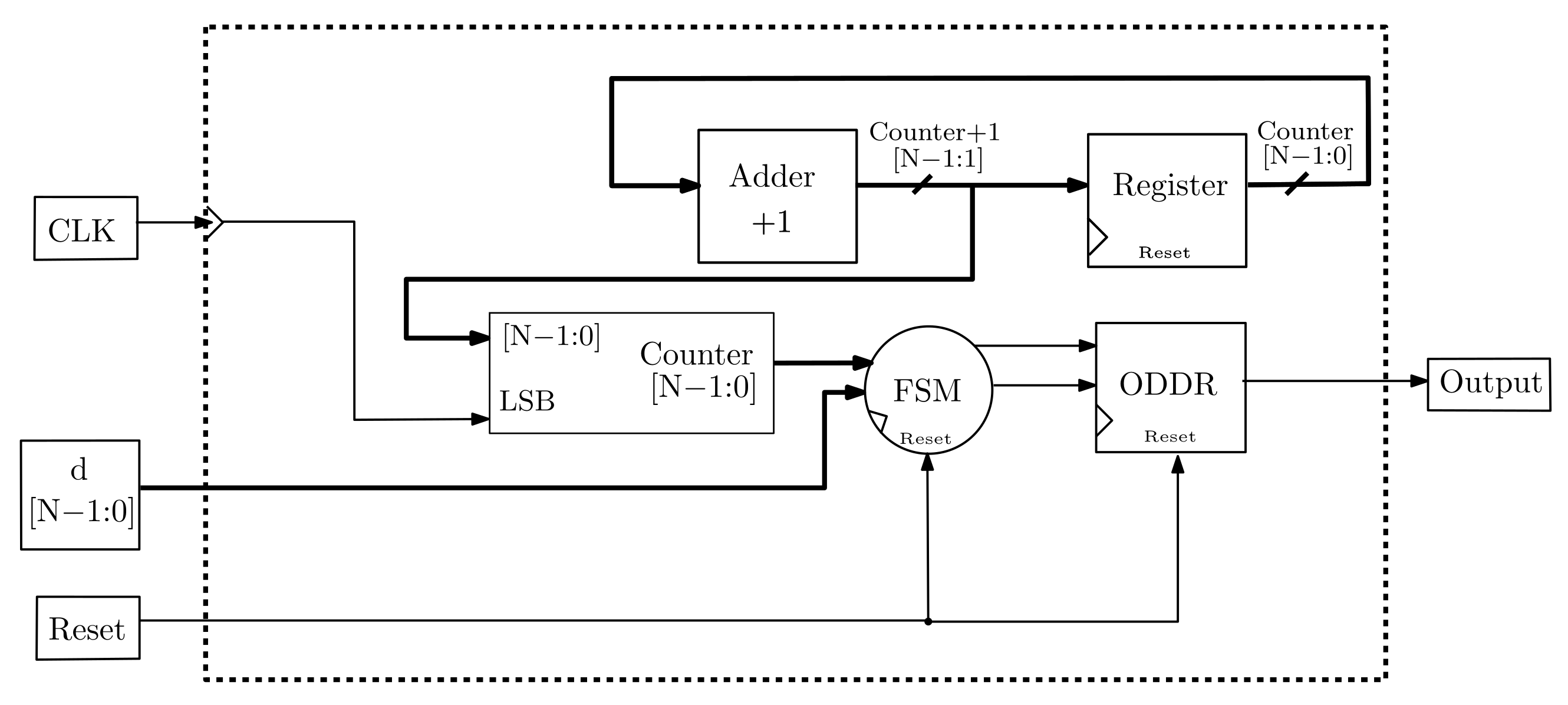
Figure 10 depicts the architecture of the N-bit DDR PWM. The least significant bit of the counter is the clock signal, and the rest of the counter bits are stored in a register. The FSM generates the two logic levels for the ODDR flip-flop, which synchronously drives the output levels at the rising and falling edges of the clock.
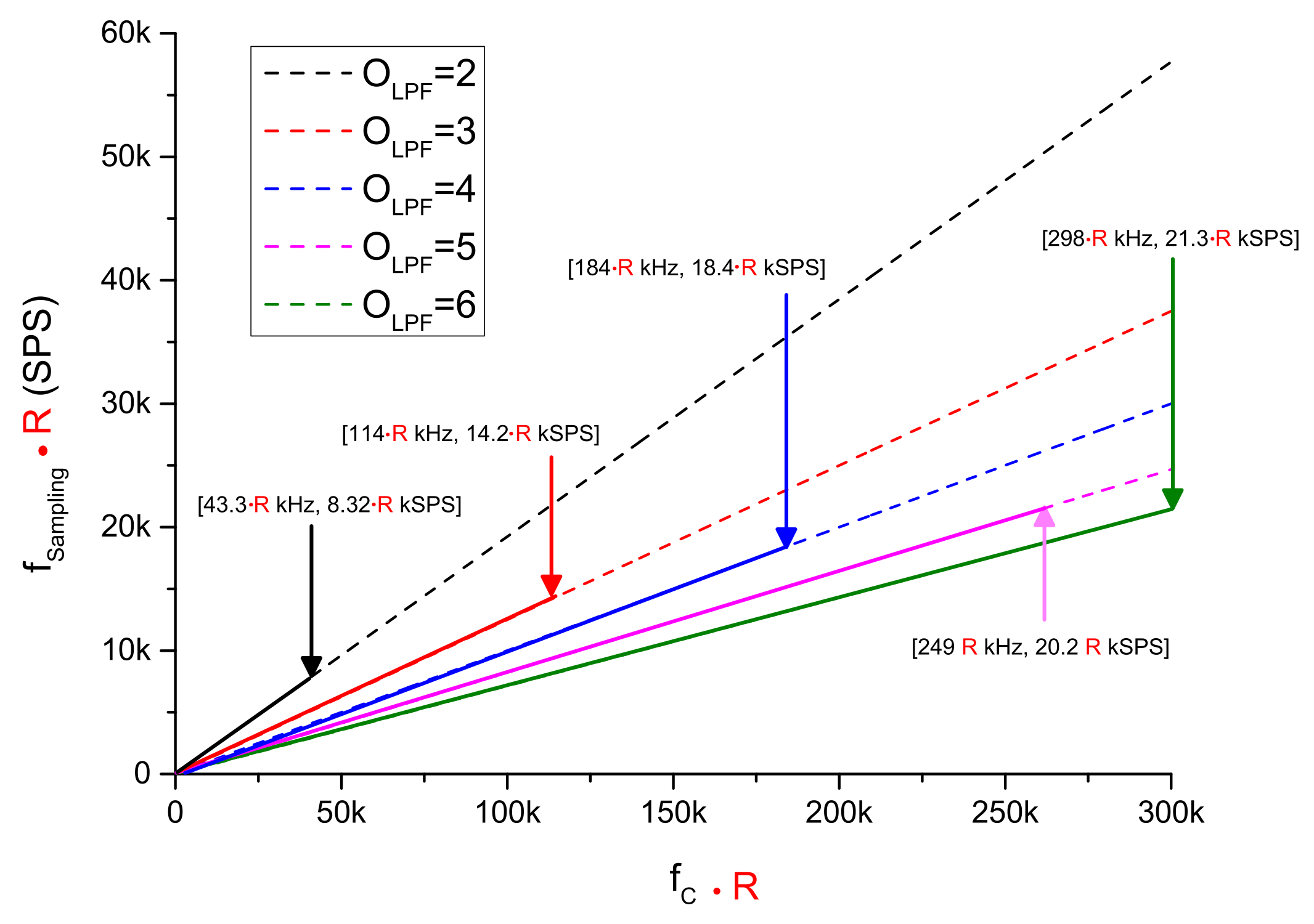
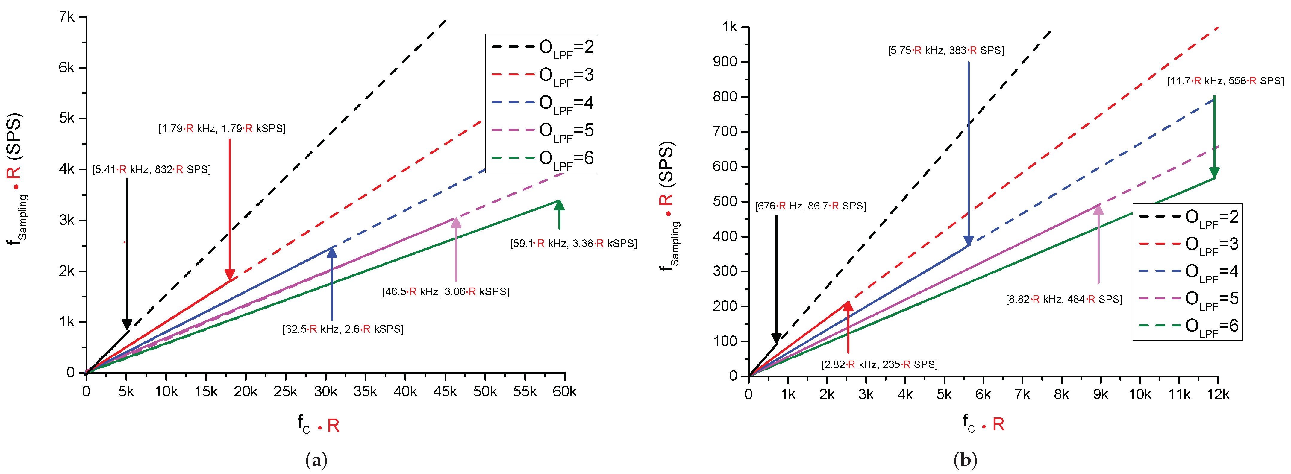
Figure 11 shows allowed solutions of f S a m p l i n g and f C for different O L P F in the 8-bit ADC with a f C L K = 100 MHz and DDR-PWM, using Equation (17). Figure 12a,b presents the f S a m p l i n g and f C solutions for 10-bit and 12-bit ADCs, respectively, with a f C L K = 100 MHz and DDR-PWM.

5. Paralleled PWM

Another way to enhance the ADC f S a m p l i n g is by a parallel design of the PWM to increase the f P W M . The N-bit PWM is divided into a set of K PWM blocks, each one built around an N K -bit counter. Therefore, the divided PWM reduces greatly the number of required counts, increasing the f P W M from Equation (6) by a factor 2 N K ( K 1 ) , as expressed in Equation (18).
f P W M K = f c l k 2 N K = f c l k 2 N · 2 N K N = 2 N K ( K 1 ) · f P W M
Due to the change on the PWM frequency, the Equation (13) has to be modified, as shown on Equation (19).
O L P F · log 10 f c l k 2 ( N K ) · f C < log 10 π 4 · 1 2 N f C f c l k < π O L P F 2 N K + N + 2 O L P F
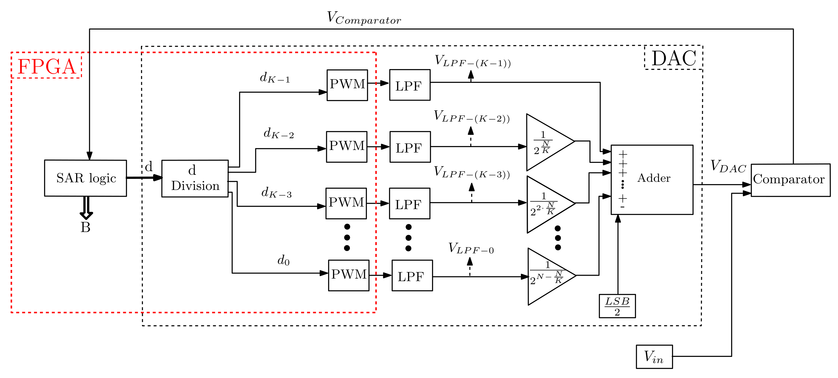
Figure 13 shows the paralleled N-bit PWM architecture. The input d of the PWM is divided as shown in Figure 14, where each subset d j ( 0 j K 1 ) is composed of a N K -bit slice of the input. Each d j drives a N K -bit PWM, generating the V D A C from the weighted addition of the filtered PWM outputs.
In order to calculate the V D A C expression, firstly, Equation (20) is obtained by replacing d to the set of d j from Equations (2)–(4). Then, Equation (7) is applied to compute the continuous coefficient of the filtered voltage for each N K -bit PWM, as expressed in Equation (21). Finally, Equation (22) is obtained from the previous two equations, which provides the weights of the addition of the V D A C .
V D A C = Δ V O d K 1 · 2 N K · ( K 1 ) 2 N + · · · + d 1 · 2 N K 2 N + d 0 2 N L S B 2 V D A C = Δ V O · j = 0 K 1 2 N K · j 2 N · d j L S B 2
V L P F j = A 0 j = Δ V O · d j 2 N K
V D A C = j = 0 K 1 2 N K · ( j + 1 ) 2 N · V L P F j L S B 2 = j = 0 K 1 2 N K · j 2 N N K · V L P F j L S B 2 V D A C = V L P F ( K 1 ) + j = 0 K 2 2 N K · j 2 N N K · V L P F j L S B 2
Although the previous description applies when the division N K is an integer value, it can be extended if it is not the case. If we denote P 1 and P 2 as integers that accomplish N = P 2 + P 1 · ( K 1 ) , the distributed PWM is composed of one P 2 -bit PWM and a set of K 1 P 1 -bit PWMs. Assuming the P 2 -bit PWM is associated to the ( K 1 ) LPF, the weighted addition is expressed in Equation (23).
V D A C = 2 P 2 + P 1 · ( K 1 ) 2 N · V L P F ( K 1 ) + j = 0 K 2 2 P 1 · ( j + 1 ) 2 N · V L P F j L S B 2 V D A C = V L P F ( K 1 ) + j = 0 K 2 2 P 1 · ( j + 1 ) 2 N · V L P F j L S B 2
As K is increased, the f C can be increased to improve f S a m p l i n g , and the O L P F can be decreased to reduce the filter complexity, at the expense of augmenting the numbers of devoted FPGA pins and filters. The extreme case is when K = N , which provides a set of K 1-bit PWMs as the solution. Nevertheless, PWMs and LPFs are unnecessary in such a case since the weighted addition of the d j is equivalent to a R-2R ladder DAC [56,57].
Figure 15 shows the allowed solutions of f S a m p l i n g and f C for different O L P F in the 8-bit ADC with f C L K = 100 MHz and the paralleled PWM with K = 2. Figure 16a,b shows f S a m p l i n g solutions for a 10-bit and 12-bit ADCs, respectively, with the same parameters.

6. Distributed Duty-Cycle PWM

This section presents an optimization focused on enhancing the f C , instead of incrementing the f P W M directly as in the previous optimizations.
The filtered PWM signal must ensure Δ V L P F < L S B at f P W M to properly perform the comparison against V i n . The Δ V L P F is dominated by the first harmonic of the PWM output, which is maximal when D = 1 2 . Reducing Δ V L P F can be used to increase the f C , which reduces the t S e t t l i n g for higher performance. Additionally, the filter order can also be reduced to provide a simpler implementation. Distributed duty cycle PWMs were implemented in applications as NPC inverters or adjustable losses distribution [58,59,60], but not in ADCs to reduce Δ V L P F .
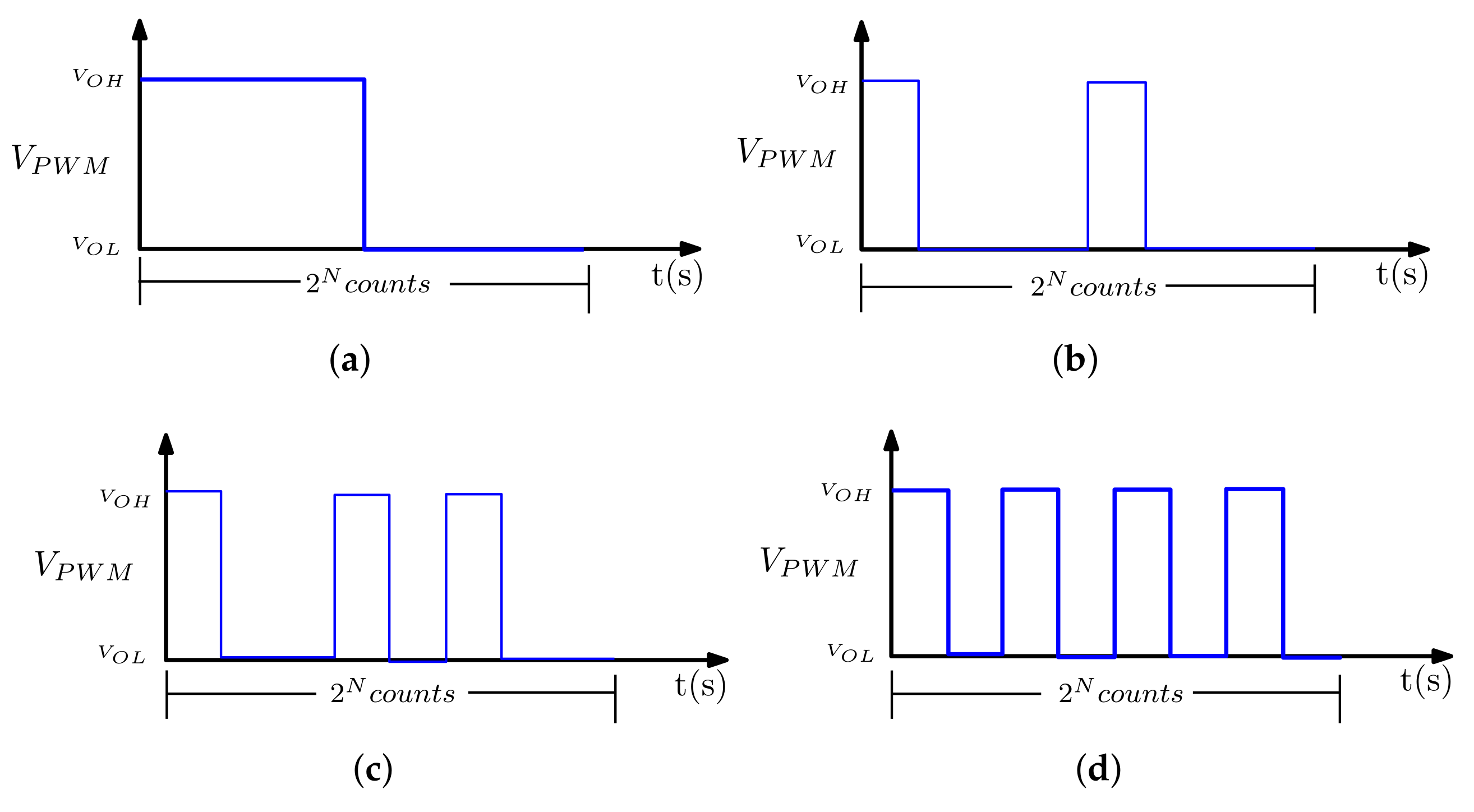
For the sake of clarity, Figure 17a shows a 3-bit PWM at D = 1 2 ; consequently, during one half of the period count, the signal is asserted. In order to significantly reduce Δ V L P F , the distributed duty cycle PWM (DDC-PWM) minimizes the elapsed time between assertions, distributing the assertions during the 2 N counts that compose a PWM period, as shown in Figure 17b–d. for D = 2 8 , 3 8 and 4 8 , respectively.
Figure 18 shows the filtered output V L P F comparison for a 3-bit PWM and DDC-PWM at D = 3 8 using the same LPF parameters, showing that the Δ V L P F is significantly reduced.
The distribution of the duty cycle increments the modulation frequency of the PWM ( f P W M D D C ) [61,62,63,64]. The maximum f P W M D D C is achieved at the condition D = 1 2 , which minimizes the first harmonic A 1 of the PWM output. Contrary to the PWM, which achieves the maximum A 1 at D = 1 2 , the maximum A 1 in the DDC-PWM is achieved at the condition D = 1 2 N or D = 2 N 1 2 N , which equals the f P W M D D C to f P W M [65,66,67]. Applying Equation (7) at the condition D = 1 2 N , the maximum first harmonic for DDC-PWM is obtained in Equation (24).
A 1 D D C ( m a x ) = 2 · Δ V O π · sin π 2 N
The upper limit for the LPF gain is obtained at f P W M D D C = f P W M in Equation (25).
A L P F ( f P W M D D C ) < π 4 · 1 2 N · 1 sin ( π 2 N )
Following the same steps that were applied in Equation (13), filter solutions for the DDC-PWM are calculated in Equation (26)
O L P F · log 10 f c l k 2 N · f C < log 10 π 4 · 1 2 N · 1 sin ( π 2 N ) f C f c l k < π O L P F [ 2 2 + N + N · O L P F O L P F ] · [ sin π 2 N 1 O L P F ]
The previous equation can be simplified by applying the small-angle approximation for sine, sin Θ Θ , leading to Equation (27)
f C f c l k < 1 2 2 + N · O L P F O L P F
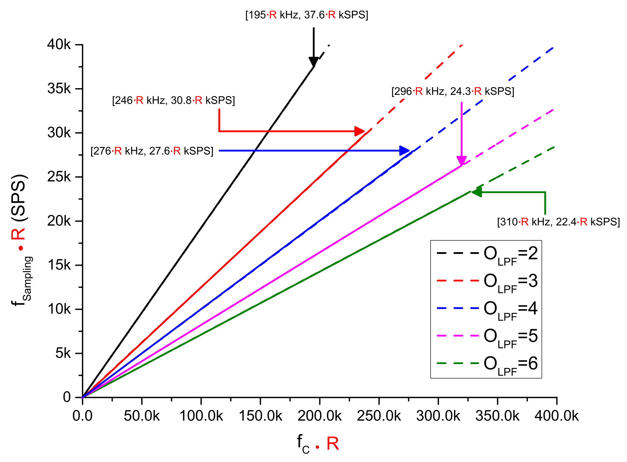
Figure 19 and Figure 20a,b show allowed solutions of f S a m p l i n g and f C for different O L P F in the 8-bit, 10-bit and 12-bit ADCs, respectively, with a f C L K = 100 MHZ and using DDC-PWM.

7. Paralleled DDR and DDC PWM

The distributed duty cycle PWM can be combined with the paralleled PWM and the DDR optimizations to enhance the f S a m p l i n g of the ADC. Combining the DDC-PWM and the DDR-PWM, Equation (27) is modified to Equation (28), which can be used to increment the f S a m p l i n g by augmenting the f C of the filter.
f C f c l k < 2 2 2 + N · O L P F O L P F
The DDC-PWM can also be combined with the paralleled PWM. The DDC-PWM can be implemented from a set of K N K -bit DDC-PWMs to improve the f S a m p l i n g . The maximum magnitude of the first harmonic is reduced from Equation (24), to Equation (29). This will lead to the improvement of the LPF solutions, according to Equation (30).
A 1 D D C ( m a x ) = 2 · Δ V O π sin π 2 N K
f C f c l k < 2 N O L P F · K 2 N + 2 O L P F + N K
Finally, Equation (31) shows the LPF solutions when there are applied the three optimizations together.
f C f c l k < 2 1 + N O L P F · K 2 N + 2 O L P F + N K
The resolution and sampling frequency of a set of ADCs on a target FPGA can be individually adjusted to the requirements of the application. This work introduces different optimization on the PWM module to improve the ADC f S a m p l i n g performance. The adoption of DDR and DDC-PWM enhances the ADC f S a m p l i n g performance without requiring additional external components for the filters and the analog comparator; however, they devote more internal FPGA resources. On the contrary, the paralleled PWM increases the number of external components and devoted FPGA pins, but the f S a m p l i n g performance can be greatly enhanced.
Figure 21a,b shows the LPF solutions for a fixed filter order O L P F = 3 and O L P F = 5, respectively, in order to implement an 8-bit ADC. The best f S a m p l i n g is obtained by combining DDR-PWM and DDC-PWM on a non-paralleled (K = 1) or paralleled PWM (K = 2, K = 4).
The paralleled PWM greatly enhances the ADC f S a m p l i n g since it leads to obtain the LPF solution with lower f C . However, the set of K N K -bit PWMs requires K + 1 FPGA input/output and additional external components for the filters. Table 3 shows the maximum f S a m p l i n g achieved and the external components required to implement the 8-bit ADC for different K, using fixed order ( O L P F = 3 and O L P F = 5 ) filters. Implementing the O L P F = 3 filter requires an operational amplifier (OA), three resistors (R) and capacitors (C) attached to a FPGA output, while for implementing the O L P F = 5 filter, two operational amplifiers, five resistors and capacitors are required. The additional OA and K + 3 resistors are devoted to implement the analog adder for the filtered outputs shift voltage 1 2 L S B , and the comparator attached to a FPGA input.

8. Experimental Results

The experimental results shown were obtained implementing 8-bit ADCs on a FPGA from Xilinx Zynq-7000 driven by f c l k = 100 MHz, with the output ports configured to obtain Δ V O = 3.3 V ( L S B = 12.89 mV). The FPGA development board is a ZedBoard Zynq 7000, which is connected with an external prototyping board containing the filters and the analog adder and comparator. The LPFs and adder are implemented using LT1364 operation amplifiers from Analog Devices [68] due to their bandwidth and slew-rate features. To implement the comparator, we used the MAX9691EPA from Analog Devices due to the fast response.

8.1. Implementation of an 8-Bit ADC with 8-Bit DDR-PWM and LPF

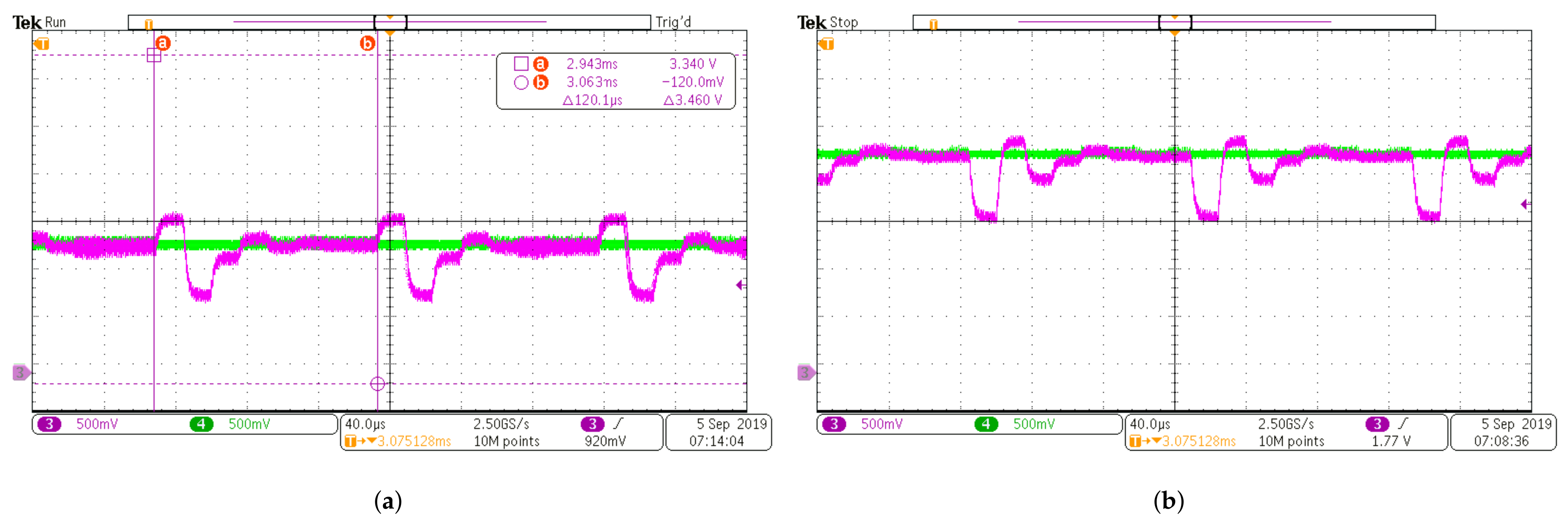
The desired f S a m p l i n g is 8 kSPS; f C is obtained from Equation (17) with minimum O L P F . The parameter values of Figure 22 show solutions of f S a m p l i n g and f C with different O L P F . Figure 22 is the same as Figure 11, but with the addition of the 8 kSPS restriction. The ADC obtained is shown in Table 4. Figure 23a,b V D A C represents the experimental results for V i n = 1.2 V and V i n = 2.2 V, respectively.
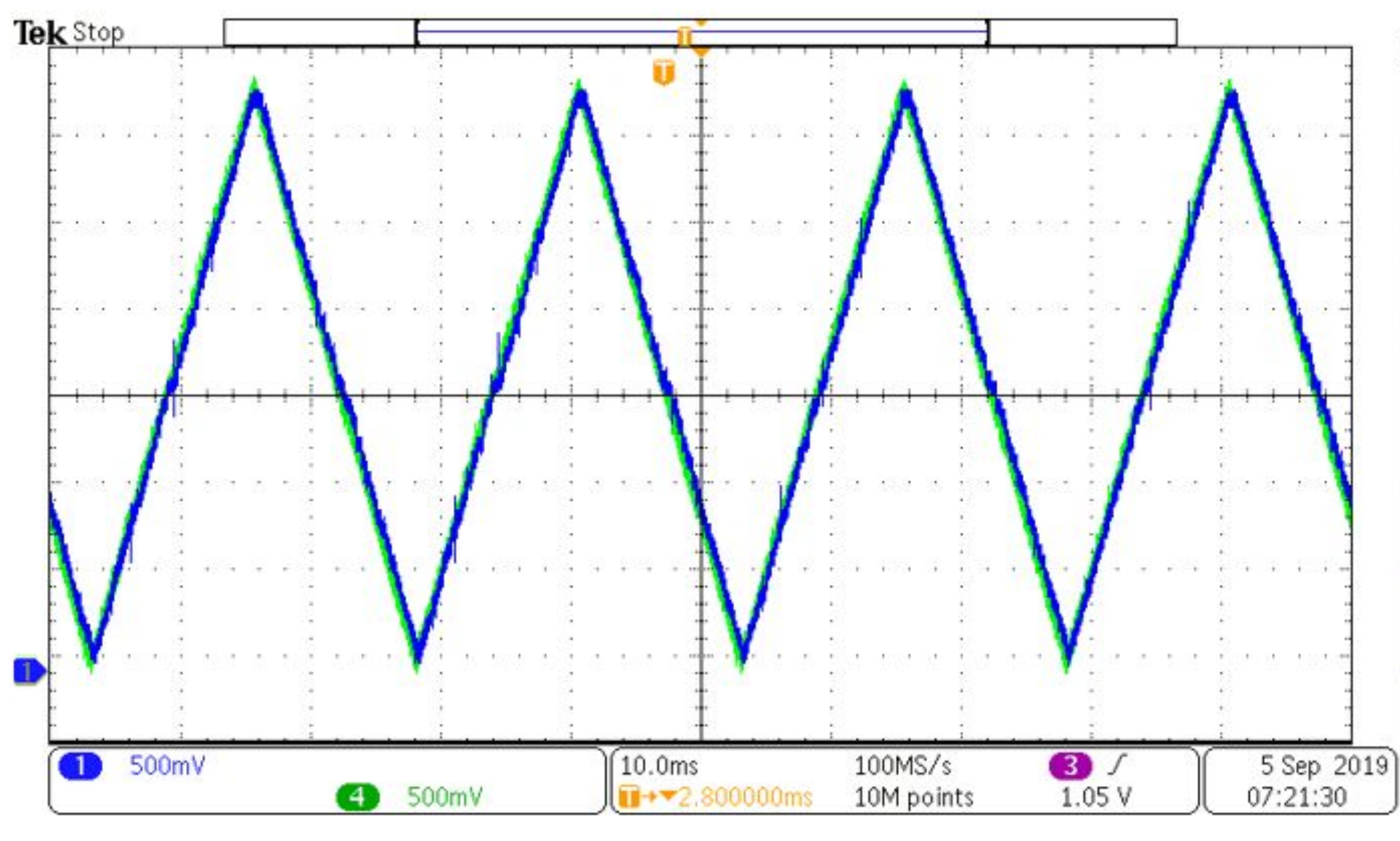
To observe B for every possible V i n value, a triangular signal of V i n is generated from 0 V to 3.3 V, with a slope that increments L S B during the conversion time ( N · t S e t t l i n g ). Figure 24 shows how B (green signal) follows the triangular signal V i n (blue signal). To show B, an extra DAC is implemented, and once the conversion is done, B is sent to the DAC.

8.2. Implementation of an 8-Bit ADC with 2 4-Bit DDC-PWM and DDR-PWM

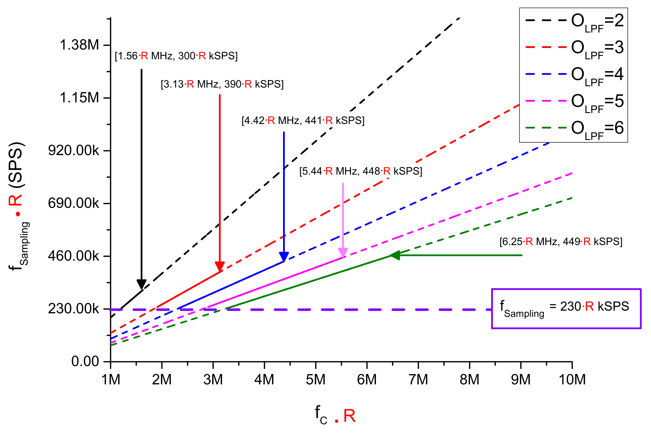
An 8-bit ADC with f S a m p l i n g = 230 kSPS is design using DDC-PWM and DDR-PWM. The implementation schematic is presented in Figure 25 where an extra DAC is added to show the obtained B. To implement the filters and the adder, the LT1364 from Analog Devices is used. Figure 26 shows the solutions of f S a m p l i n g and f C with different O L P F . For designing the LPF, the minimum O L P F that accomplishes the desired f S a m p l i n g is chosen. O L P F = 2 is chosen to implement the LPF, and the parameters values are shown in Table 5.
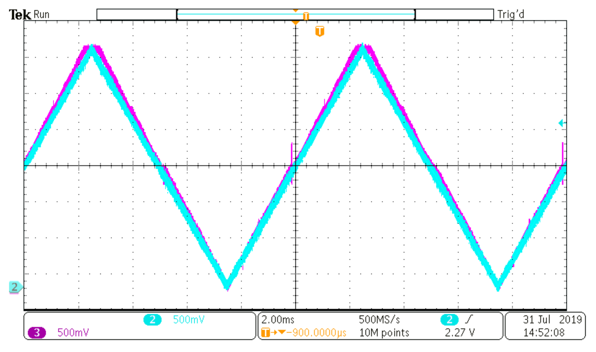
Figure 27 shows V D A C behavior for a fixed V i n of 2.2 V. Figure 28 shows B (pink signal) for every possible V i n (blue signal).

8.3. Implementation of an 8-Bit ADC with 4 2-Bit DDC-PWM and DDR-PWM

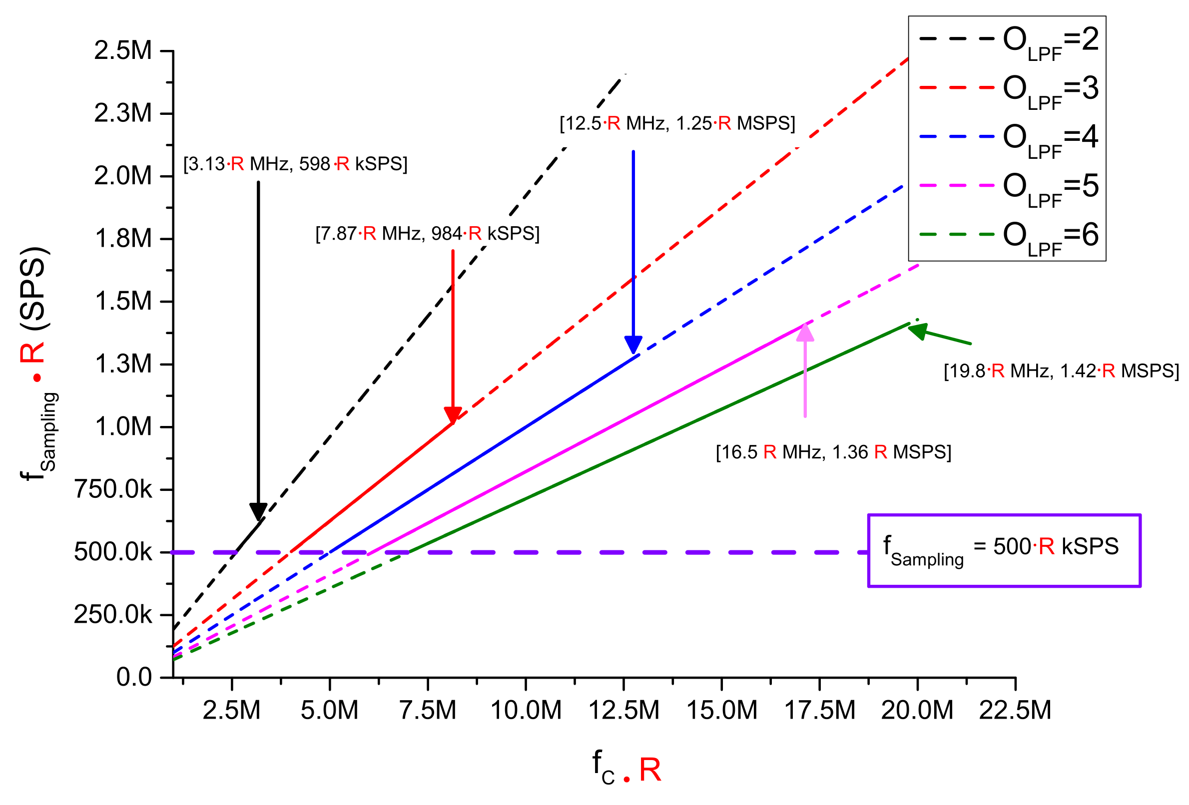
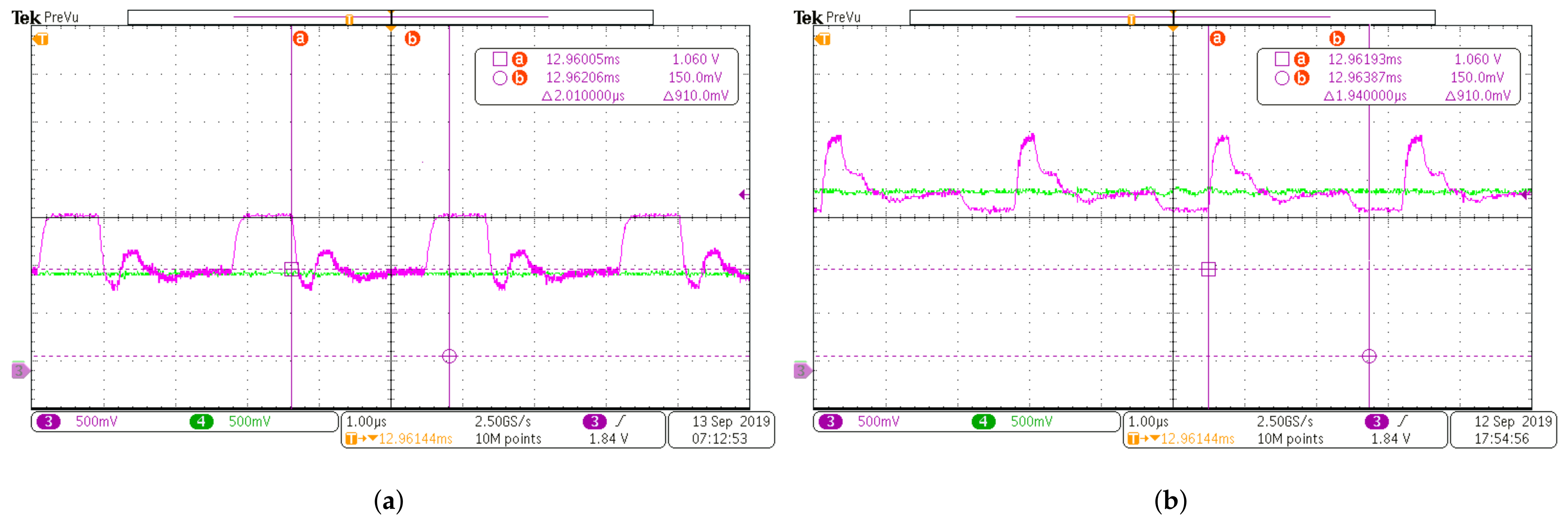
An 8-bit ADC with f S a m p l i n g = 500 kSPS is designed, using 4 2-bit DDC-PWM and DDR-PWM. The schematic is presented in Figure 29 with the extra DAC for visualization. The LPF and adder will be implemented with the OA LT1364. Figure 30 shows the LPF parameters found out, where it can be seen that with an O L P F = 2 the desired f S a m p l i n g can be accomplished. Figure 31a,b shows V D A C for a fixed V i n of 1 V and 1.8 V, respectively. Figure 32 shows B (pink signal) for every possible value of V i n (blue signal).

9. Discussion

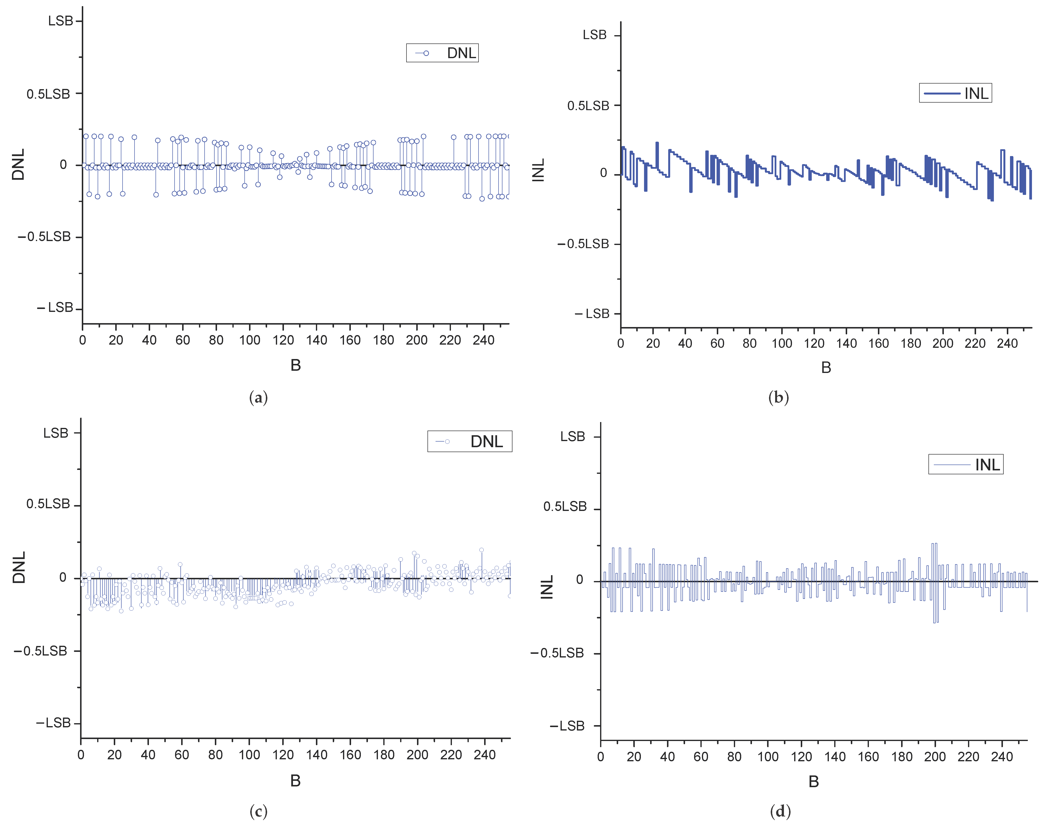
One of the main characteristic from the ADCs are DNL (differential non-linearity) and INL (integral non-linearity). The DNL is defined as the difference in the step width between the ADC response and the ideal response, while the INL is defined as the deviation of the ADC response curve from the ideal response curve, both are expressed in LSB. To calculate and simulate the DNL from the proposed ADC, the 8-bit ADC with K = 4 DDC-PWM and DDR-PWM presented in the last section is selected. The DNL is showed on Figure 33a, while Figure 33b shows the INL. Figure 33c,d show DNL and INL, respectively, for an 8-bit ADC with K = 2 DDC-PWM and DDR-PWM.
Another characteristic from the ADCs is the ENOB. The ENOB is an indicator of the ADC resolution at a specific input frequency and f S a m p l i n g . To calculate ENOB, Equation (32) is used, where SNDR is the signal-to-noise-and-distortion ratio as showed in [38].
ENOB = SNDR 1.76 6.02
Table 6 compares related ADC from the state of the art with the proposed ADC, using K = 4 and K = 2. The proposed ADCs, even though they do not provide high sampling rates, are parametrizable and portable to any FPGA family. Table 7 compares the proposed ADC with different resolution (10-bit and 12-bit) with different implementation method (K = N 2 and K = 2).

10. Conclusions

This work presents an scalable and parametrizable implementation architecture for analog-to-digital converters (ADC) on field programmable gate array (FPGA) devices. The ADC is based on successive approximation register (SAR) and the digital-to-analog converter (DAC) is implemented by a pulse-width modulator (PWM) and a low-pass filter (LPF). The paper presents a systematic method to implement the ADC based on the FPGA parameters as clock frequency ( f c l k ) and FPGA output voltage ( Δ V O ) and allowing the designer to find different solutions to implement the LPF that meet the ADC resolution bits (N) and sampling frequency ( f S a m p l i n g ) required for the application.
Three improvements of the PWM are also presented in order to enhance the sampling frequency ( f S a m p l i n g ) of ADCs. The double data rate (DDR) PWM focuses on increasing the PWM frequency ( f P W M ) to enhance the f S a m p l i n g . The paralleled PWM also focuses on increasing the f P W M by using a set of K N K -bit PWMs. The f S a m p l i n g is significantly increased in the paralleled PWM, but it requires a set of K filters and the weighted addition of their filtered outputs, which increases the number of external components. The last presented improvement is the distributed duty cycle (DDC) PWM, which focus on decreasing the required cutoff frequency ( f C ) of the filter by the distribution of the PWM assertions of the duty cycle to reduce the peak-to-peak filtered output.
The paralleled PWM greatly improves f S a m p l i n g at the expense of increasing the complexity of the external circuits. On the contrary, the DDR and DDC PWM improvements do not require additional external circuits, but the f S a m p l i n g gain is more limited. Depending on the number of ADCs and the application requirements, the three PWM improvements can be combined to increase the ADC performance. The methodology and PWM improvements were tested on a Zynq-7000 device, but they can be directly applied to different FPGA families.

Author Contributions

Conceptualization, E.C.N. and E.V.-I.; methodology, J.D.E.C.; software, E.C.N. and J.D.E.C.; validation, J.D.E.C., E.C.N. and E.V.-I.; formal analysis, E.V.-I.; investigation, E.V.-I. and E.C.N.; resources, J.D.E.C.; data curation, E.C.N. and E.V.-I.; writing—original draft preparation, J.D.E.C.; writing—review and editing, E.V.-I. and E.C.N.; visualization, J.D.E.C. and E.V.-I.; supervision, E.C.N. and E.V.-I.; project administration, E.V.-I.; funding acquisition, E.V.-I. All authors have read and agreed to the published version of the manuscript.

Funding

This work was supported by the Spanish MINISTERIO DE CIENCIA E INNOVACIÓN under research projects PID2020-120151RB-I00, funded by MCIN/ AEI /10.13039/501100011033.

Conflicts of Interest

The authors declare no conflict of interest.

Abbreviations

The following abbreviations are used in this manuscript:
NBit resolution
ADCAnalog-to-digital converter
DACDigital-to-analog converter
LPFLow pass filter
PWMPulse width modulation
f C Cutoff frequency
O L P F LPF order
SARsuccessive approximation register
f S a m p l i n g ADC sampling frequency.
f C L K Clock frequency
LSBLess significant bit
DDRDouble data rate
DDCDistributed duty cycle

References

  1. Sakanushi, T.; Yamada, K.; Matsuura, S.; Hagiwara, T.; Aando, Y.; Murakami, I. A design method for two-degree-of-freedom simple repetitive control systems for multiple-input/multiple-output plants. In Proceedings of the 2010 World Automation Congress, Kobe, Japan, 19–23 September 2010; pp. 1–6. [Google Scholar]
  2. Ang, G.J.; Lim, W.Z.; Lim, C.M. A proposed two-input two-output self-tuning control scheme. In Proceedings of the 2018 IEEE Symposium on Computer Applications Industrial Electronics (ISCAIE), Penang, Malaysia, 28–29 April 2018; pp. 102–107. [Google Scholar]
  3. Zhang, J.; Kuai, Y.; Zhou, S.; Hou, G.; Ren, M. Improved minimum entropy control for two-input and two-output networked control systems. In Proceedings of the 2016 UKACC 11th International Conference on Control, Belfast, UK, 31 August–2 September 2016; pp. 1–5. [Google Scholar]
  4. Ren, M.; Zhang, J.; Jiang, M.; Yu, M.; Xu, J. Minimum (h,ϕ)—Entropy Control for Non-Gaussian Stochastic Networked Control Systems and Its Application to a Networked DC Motor Control System. IEEE Trans. Control Syst. Technol. 2014, 23, 406–411. [Google Scholar] [CrossRef]
  5. Cruz-Miguel, E.E.; García-Martínez, J.R.; Rodríguez-Reséndiz, J.; Carrillo-Serrano, R.V. A New Methodology for a Retrofitted Self-tuned Controller with Open-Source FPGA. Sensors 2020, 20, 6155. [Google Scholar] [CrossRef] [PubMed]
  6. Sudharsan, R.R. Synthesis of FIR Filter using ADC-DAC: A FPGA Implementation. In Proceedings of the 2019 IEEE International Conference on Clean Energy and Energy Efficient Electronics Circuit for Sustainable Development (INCCES), Krishnankoil, India, 18–20 December 2019; pp. 1–3. [Google Scholar] [CrossRef]
  7. Yau, Y.-T.; Hwu, K.-I.; Shieh, J.-J. Applying FPGA Control with ADC-Free Sampling to Multi-Output Forward Converter. Electronics 2021, 10, 1010. [Google Scholar] [CrossRef]
  8. Rodríguez-Reséndiz, J.; Mendoza-Mondragón, F.; Gómez-Loenzo, R.A.; Martínez-Hernández, M.A.; Mucino, V.H. An approach to motion control applications based on advanced programmable devices. Int. J. Electr. Eng. Educ. 2012, 49, 243–259. [Google Scholar] [CrossRef]
  9. Cruz-Miguel, E.E.; Rodríguez-Reséndiz, J.; García-Martínez, J.R.; Camarillo-Gómez, K.A.; Pérez-Soto, G.I. Field-programmable gate array-based laboratory oriented to control theory courses. Comput. Appl. Eng. Educ. 2019, 27, 1253–1266. [Google Scholar] [CrossRef] [Green Version]
  10. Sahu, N.; Londhe, N.D.; Kshirsagar, G.B. FPGA applications in inverter and converter circuits: A review on technology, benefits and challenges. In Proceedings of the 2017 International Conference on Innovations in Information, Embedded and Communication Systems (ICIIECS), Coimbatore, India, 17–18 March 2017. [Google Scholar]
  11. Dhede, O.S.; Shah, S.K. A review: Hardware Implementation of AES using minimal resources on FPGA. In Proceedings of the 2015 International Conference on Pervasive Computing (ICPC), Pune, India, 8–10 January 2015; pp. 1–3. [Google Scholar]
  12. Ni, M.; Wang, X.; Li, F.; Rhee, W.; Wang, Z. A 13-Bit 2-GS/s Time-Interleaved ADC with Improved Correlation-Based Timing Skew Calibration Strategy. IEEE Trans. Circuits Syst. I Regul. Pap. 2021, 69, 481–494. [Google Scholar] [CrossRef]
  13. Nam, J.; Hassanpourghadi, M.; Zhang, A.; Chen, M.S. A 12-Bit 1.6, 3.2, and 6.4 GS/s 4-b/Cycle Time-Interleaved SAR ADC with Dual Reference Shifting and Interpolation. IEEE J. -Solid-State Circuits 2018, 53, 1765–1779. [Google Scholar] [CrossRef]
  14. Devarajan, S.; Singer, L.; Kelly, D.; Pan, T.; Silva, J.; Brunsilius, J.; Rey-Losada, D.; Murden, F.; Speir, C.; Bray, J.; et al. A 12-b 10-GS/s Interleaved Pipeline ADC in 28-nm CMOS Technology. J. -Solid-State Circuits 2017, 52, 3204–3218. [Google Scholar] [CrossRef]
  15. Zhou, Y.; Xu, B.; Chiu, Y. A 12-b 1-GS/s 31.5-mW Time-Interleaved SAR ADC with Analog HPF-Assisted Skew Calibration and Randomly Sampling Reference ADC. IEEE J. -Solid-State Circ. 2019, 54, 2207–2218. [Google Scholar] [CrossRef]
  16. Monteiro, V.; Ferreira, J.C.; Melendez, A.A.N.; Afonso, J.A.; Couto, C.; Afonso, J.L. Experimental Validation of a Bidirectional Three-Level dc-dc Converter for On-Board or off-Board EV Battery Chargers. In Proceedings of the IECON 2019—45th Annual Conference of the IEEE Industrial Electronics Society, Lisbon, Portugal, 14–17 October 2019. [Google Scholar]
  17. Kim, B.; Kim, H.; Choi, S. Three-phase on-board charger with three modules of single-stage interleaved soft-switching AC-DC converter. In Proceedings of the 2018 IEEE Applied Power Electronics Conference and Exposition (APEC), San Antonio, TX, USA, 4–8 March 2018; pp. 3405–3410. [Google Scholar]
  18. Kamble, A.S.; Swami, P.S. On-Board Integreted Charger for Electric Vehicle Based on Split Three Phase Insuction Motor. In Proceedings of the 2018 International Conference on Emerging Trends and Innovations In Engineering and Technological Research (ICETIETR), Ernakulam, India, 1–13 July 2018; pp. 1–5. [Google Scholar]
  19. Mooney, J.; Halton, M.; Mahdi, A.E. Specialized Digital Signal Processor for control of multi-rail/multi-phase high switching frequency power converters. In Proceedings of the 2010 Twenty-Fifth Annual IEEE Applied Power Electronics Conference and Exposition (APEC), Palm Springs, CA, USA, 21–25 February 2010; pp. 2207–2211. [Google Scholar]
  20. Mooney, J.; Effler, S.; Halton, M.; Mahdi, A.E. DSP-based control of multi-rail DC-DC converter systems with non-integer switching frequency ratios. In Proceedings of the 2010 1st International Conference on Energy, Power and Control (EPC-IQ), Basrah, Iraq, 30 November–2 December 2010; pp. 203–207. [Google Scholar]
  21. Rahimi, A.A.; Carreira, L.B.; Gupta, S. Synchronous multi-signal acquisition for WBSNs using gold-code based joint-compressive sensing. In Proceedings of the 2016 IEEE Biomedical Circuits and Systems Conference (BioCAS), Shanghai, China, 17–19 October 2016; pp. 236–239. [Google Scholar]
  22. Man, X.; Wu, L.; Zhang, X.; Ma, T.; Jia, W. A High Precision Multi-Cell Battery Voltage Detecting Circuit for Battery Management Systems. In Proceedings of the 2016 IEEE 83rd Vehicular Technology Conference (VTC Spring), Nanjing, China, 15–18 May 2016; pp. 1–5. [Google Scholar]
  23. Amitkumar, K.S.; Narayanan, G. Simplified implementation of space vector PWM strategies for a three level inverter. In Proceedings of the 2012 IEEE 7th International Conference on Industrial and Information Systems (ICIIS), Chennai, India, 6–9 August 2012; pp. 1–6. [Google Scholar]
  24. Lopatkin, N.N. Voltage source multilevel inverter voltage quality comparison under multicarrier sinusoidal PWM and space vector PWM of two delta voltages. In Proceedings of the 2017 International Multi-Conference on Engineering, Computer and Information Sciences (SIBIRCON), Novosibirsk, Russia, 18–22 September 2017; pp. 439–444. [Google Scholar]
  25. Devi, V.S.K.; Srivani, S.G. Modified phase shifted PWM for cascaded H bridge multilevel inverter. In Proceedings of the 2017 Third International Conference on Advances in Electrical, Electronics, Information, Communication and Bio-Informatics (AEEICB), Chennai, India, 27–28 February 2017; pp. 89–94. [Google Scholar]
  26. Jeon, M.-K.; Yoo, W.-J.; Kim, C.-G.; Yoo, C. A Stochastic Flash Analog-to-Digital Converter Linearized by Reference Swapping. IEEE Access 2017, 5, 23046–23051. [Google Scholar] [CrossRef]
  27. Fahmy, A.; Liu, J.; Kim, T.; Maghari, N. An All-Digital Scalable and Reconfigurable Wide-Input Range Stochastic ADC Using Only Standard Cells. IEEE Trans. Circuits Syst. II Express Briefs 2015, 62, 731–735. [Google Scholar] [CrossRef]
  28. Weaver, S.; Hershberg, B.; Moon, U. Digitally Synthesized Stochastic Flash ADC Using Only Standard Digital Cells. IEEE Trans. Circuits Syst. I Regul. Pap. 2014, 61, 84–91. [Google Scholar] [CrossRef]
  29. Unnikrishnan, V.; Pathapati, S.R.; Vesterbacka, M. A fully synthesized all-digital VCO-based analog-to-digital converter. In Proceedings of the 2015 Nordic Circuits and Systems Conference (NORCAS): NORCHIP & International Symposium on System-on-Chip (SoC), Oslo, Norway, 26–28 October 2015; pp. 1–4. [Google Scholar] [CrossRef]
  30. Unnikrishnan, V.; Vesterbacka, M. A NAND gate based standard cell VCO for use in synthesizable ADCs. In Proceedings of the 2015 Nordic Circuits and Systems Conference (NORCAS): NORCHIP & International Symposium on System-on-Chip (SoC), Oslo, Norway, 26–28 October 2015; pp. 1–4. [Google Scholar] [CrossRef]
  31. Ghozzy, S.; Ragai, H.F.; El-Nozahi, M. A Two-Step VCO-Based ADC with PWM Pre-coded Coarse Quantizer. In Proceedings of the 2020 IEEE 3rd International Conference on Electronics Technology (ICET), Chengdu, China, 8–12 May 2020; pp. 262–265. [Google Scholar] [CrossRef]
  32. Vardhini, P.A.H. Analysis of integrator for continuous time Digital sigma Delta ADC on Xilinx FPGA. In Proceedings of the 2016 International Conference on Electrical, Electronics, and Optimization Techniques (ICEEOT), Chennai, India, 3–5 March 2016; pp. 2689–2693. [Google Scholar] [CrossRef]
  33. Rajesh, G.P.; Deepthy, C.K.; Jermila, M.M.; Raghunath, K.P.; Aparna, V.N. Force Rebalance with Multi-bit Sigma-Delta implemented with FPGA for Precision Rate Sensor. In Proceedings of the TENCON 2019—2019 IEEE Region 10 Conference (TENCON), Kochi, India, 17–20 October 2019; pp. 654–657. [Google Scholar] [CrossRef]
  34. Kumar, P.S.; Narayana, D.L.; Tejesvi, V.R.; Chandrasen, M.K. FPGA based Sigma-Delta analog to digital converter for power sensing. In Proceedings of the 2016 International Conference on Electrical, Electronics, and Optimization Techniques (ICEEOT), Chennai, India, 3–5 March 2016; pp. 4912–4914. [Google Scholar] [CrossRef]
  35. Homulle, H.; Regazzoni, F.; Charbon, E. 200 MS/s ADC implemented in a FPGA employing TDCs. In Proceedings of the 2015 ACM/SIGDA International Symposium on Field-Programmable Gate Arrays, New York, NY, USA, 22–24 February 2015; pp. 228–235. [Google Scholar] [CrossRef]
  36. Homulle, H.; Visser, S.; Charbon, E. A Cryogenic 1 GSa/s, Soft-Core FPGA ADC for Quantum Computing Applications. IEEE Trans. Circuits Syst. I Regul. Pap. 2016, 63, 1854–1865. [Google Scholar] [CrossRef] [Green Version]
  37. Xiang, Z.; Wang, T.; Geng, T.; Xiang, T.; Jin, X.; Herbordt, M. Soft-Core. Multiple-Lane, FPGA-based ADCs for a Liquid Helium Environment. In Proceedings of the 2018 IEEE High Performance Extreme Computing Conference (HPEC), Waltham, MA, USA, 25–27 September 2018; pp. 1–6. [Google Scholar] [CrossRef]
  38. Leuenberger, L.; Amiet, D.; Wei, T.; Zbinden, P. An FPGA-based 7-ENOB 600 MSample/s ADC without any External Components. In Proceedings of the The 2021 ACM/SIGDA International Symposium on Field-Programmable Gate Arrays, New York, NY, USA, 28 February–2 March 2021; pp. 240–250. [Google Scholar] [CrossRef]
  39. Crovetti, P.S. All-Digital High Resolution D/A Conversion by Dyadic Digital Pulse Modulation. IEEE Trans. Circuits Syst. I Regul. Pap. 2017, 64, 573–584. [Google Scholar] [CrossRef] [Green Version]
  40. Aiello, O.; Crovetti, P.; Alioto, M. Fully Synthesizable Low-Area Analogue-to-Digital Converters with Minimal Design Effort Based on the Dyadic Digital Pulse Modulation. IEEE Access 2020, 8, 70890–70899. [Google Scholar] [CrossRef]
  41. Aiello, O.; Crovetti, P.S.; Alioto, M. Fully Synthesizable Low-Area Digital-to-Analog Converter with Graceful Degradation and Dynamic Power-Resolution Scaling. IEEE Trans. Circuits Syst. I Regul. Pap. 2019, 66, 2865–2875. [Google Scholar] [CrossRef]
  42. Aiello, O.; Crovetti, P.S.; Alioto, M. Standard Cell-Based Ultra-Compact DACs in 40-nm CMOS. IEEE Access 2019, 7, 126479–126488. [Google Scholar] [CrossRef]
  43. Xu, Z.; Ojima, N.; Li, S.; Iizuka, T. An All-Standard-Cell-Based Synthesizable SAR ADC with Nonlinearity-Compensated RDAC. IEEE Trans. Very Large Scale Integr. (Vlsi) Syst. 2021, 29, 2153–2162. [Google Scholar] [CrossRef]
  44. Wang, G.; Chiu, Y. Fast FPGA emulation of background-calibrated SAR ADC with internal redundancy dithering. In Proceedings of the IEEE 2013 Custom Integrated Circuits Conference, San Jose, CA, USA, 22–25 September 2013; pp. 1–4. [Google Scholar]
  45. Chen, M.; Zhou, C.; He, W.; Ye, F.; Junyan, R. A Split-Based Neural Network Calibrator for SAR-Pipelined ADC on FPGA. In Proceedings of the 2020 IEEE 15th International Conference on Solid-State Integrated Circuit Technology (ICSICT), Kunming, China, 3–6 November 2020; pp. 1–3. [Google Scholar]
  46. Hooi, L.Y.; Hiung, L.H.; Drieberg, M.; Sebastian, P. Configurable 2 bits per cycle successive approximation register for analog to digital converter on FPGA. In Proceedings of the 2016 6th International Conference on Intelligent and Advanced Systems (ICIAS), Kuala Lumpur, Malaysia, 15–17 August 2016; pp. 1–5. [Google Scholar]
  47. Colletta, G.; Ferreira, D.; Crepaldi, P. A Successive Approximation A/D Converter Using a PWM Modulator DAC. In Proceedings of the 2012 IEEE Ninth Electronics, Robotics and Automotive Mechanics Conference, Cuernavaca, Mexico, 19–23 November 2012; pp. 333–337. [Google Scholar]
  48. David, M.A. Using PWM Output as a Digital-to-Analog Converter on a TMS320F280x Digital Signal Controller; Texas Instrument: Dallas, TX, USA, 2008; Available online: https://www.ti.com/lit/pdf/spraa88 (accessed on 30 November 2021).
  49. Nisarga, B. PWM DAC Using MSP430 High-Resolution Timer; Texas Instrument: Dallas, TX, USA, 2013; Available online: https://www.ti.com/lit/pdf/slaa497 (accessed on 30 November 2021).
  50. Lukic, Z.; Rahman, N.; Prodie, A. Multibit Σ–Δ PWM Digital Controller IC for DC-DC Converters Operating at Switching Frequencies Beyond 10 MHz. IEEE Trans. Power Electron. 2007, 5, 1693–1707. [Google Scholar] [CrossRef]
  51. Mitchell, M. Using PWM Timer B as a DAC; Texas Instrument: Dallas, TX, USA, 2008; Available online: https://www.ti.com/lit/pdf/slaa497 (accessed on 30 November 2021).
  52. Malvino, A. Principios de Electronica; McGraw-Hill: New York, NY, USA, 2007; Available online: https://books.google.es/books?id=UaxhQQfLMY8C (accessed on 30 November 2021).
  53. Mehta, R.; Jasani, H. FPGA realization of novel techniques for DDR based data acquisition system. In Proceedings of the 2016 2nd International Conference on Next Generation Computing Technologies (NGCT), Dehradun, India, 14–16 October 2016. [Google Scholar]
  54. Hamil, H.; Azzaz, M.S.; Sakhi, S.; Maali, A.; Zidelmal, Z.; Abdeslam, D.O. Design and FPGA real-time implementation of PWM and PPM modulation for Ultra Wide Band applications. In Proceedings of the 2019 6th International Conference on Image and Signal Processing and their Applications (ISPA), Mostaganem, Algeria, 24–25 November 2019; pp. 1–5. [Google Scholar]
  55. Tiwari, A. A low power high speed dual data rate acquisition system using FPGA. In Proceedings of the 2012 International Conference on Communication, Information Computing Technology (ICCICT), Mumbai, India, 19–20 October 2012; pp. 1–4. [Google Scholar]
  56. Reddy, N.U.; Babu, R.; Chaitanyakumar, M.V. A 4 bit 5GHz R-2R Digital to Analog Converter using hetrojunction HEMT. In Proceedings of the 2013 International Conference on Emerging Trends in Communication, Control, Signal Processing and Computing Applications (C2SPCA), Bangalore, India, 10–11 October 2013; pp. 1–6. [Google Scholar]
  57. Chen, C.C.; Lu, N.K. Nonlinearity analysis of R-2R ladder-based current-steering digital to analog converte. In Proceedings of the 2013 IEEE International Symposium on Circuits and Systems (ISCAS), Beijing, China, 9–23 May 2013; pp. 833–836. [Google Scholar]
  58. Radhika, V.; Baskaran, K. FPGA based DPWM/DPFM architecture for digitally controlled dc-dc converters. In Proceedings of the 2016 IEEE Uttar Pradesh Section International Conference on Electrical, Computer and Electronics Engineering (UPCON), Varanasi, India, 9–11 December 2016; pp. 78–82. [Google Scholar]
  59. Debnath, S.; Qin, J.; Saeedifard, M. A distributed PWM strategy for modular multilevel converter. In Proceedings of the IECON 2014—40th Annual Conference of the IEEE Industrial Electronics Society, Dallas, TX, USA, 29 October–1 November 2014. [Google Scholar]
  60. Hernandez, L.; Prefasi, E. Analog to digital conversion using a Pulse Width Modulator and an irregular sampling decoder. In Proceedings of the 2006 13th IEEE International Conference on Electronics, Circuits and Systems, Nice, France, 10–13 December 2006. [Google Scholar]
  61. Radhika, V.; Baskaran, K. Hybrid digital pulse width modulator architecture using FPGA. In Proceedings of the 2016 IEEE International Conference on Recent Trends in Electronics, Information Communication Technology (RTEICT), Bangalore, India, 20–21 May 2016. [Google Scholar]
  62. Sabarinath, V.; Sivanandam, K. Design and implementation of FPGA based high resolution digital pulse width modulator. In Proceedings of the 2013 International Conference on Communication and Signal Processing, Melmaruvathur, India, 3–5 April 2013. [Google Scholar]
  63. Shimazoe, K.; Takahashi, H.; Shi, B.; Furumiya, T.; Ooi, J.; Kumazawa, Y.; Murayama, H. Novel Front-End Pulse Processing Scheme for PET System Based on Pulse Width Modulation and Pulse Train Method. IEEE Trans. Nucl. Sci. 2010, 57, 782–786. [Google Scholar] [CrossRef]
  64. Zrilic, D.G. Alternative Approach to Use of Pulse Width Modulation. In Proceedings of the 2006 World Automation Congress, Budapest, Hungary, 24–26 July 2006. [Google Scholar]
  65. Lin, H.; Chen, R.; Li, R.; Zhu, L.; Yan, H.; Shu, Z. A Flexible and Fast Space Vector Pulse Width Modulation Technique for Multilevel Converters. In Proceedings of the 2019 22nd International Conference on Electrical Machines and Systems (ICEMS), Harbin, China, 11–14 August 2019; pp. 1–4. [Google Scholar]
  66. Salomon, L.; Moreno, R.; Pimenta, T. Implementation of a 17 bits Pulse Width Modulation circuit using FPGA. In Proceedings of the 2015 27th International Conference on Microelectronics (ICM), Casablanca, Morocco, 20–23 December 2015. [Google Scholar]
  67. Lee, Y.; Lee, J.; Kim, J. GaN FET-based synchronous buck converter with 10-bit 4-MHz digital pulse width modulator. In Proceedings of the 2015 9th International Conference on Power Electronics and ECCE Asia (ICPE-ECCE Asia), Seoul, Korea, 1–5 June 2015. [Google Scholar]
  68. LT1364 Dual and Quad 70 MHz, 1000V/µs Op Amps. LT1364 Datasheet LINEAR TECHNOLOGY CORPORATION. 2013. Available online: https://www.analog.com/media/en/technical-documentation/data-sheets/13645fa.pdf (accessed on 30 November 2021).
Figure 1. V D A C and V i n for an 8-bit SAR-based ADC.
Electronics 11 00447 g001
Figure 2. Block diagram of SAR-based ADC with DAC implemented with PWM and LPF.
Electronics 11 00447 g002
Figure 3. Schematic of the N-bit PWM.
Electronics 11 00447 g003
Figure 4. (a) Magnitude plot of the LPF frequency response. (b) Normalized step response at f C = 1 Hz for different O L P F .
Electronics 11 00447 g004
Figure 5. f C vs. f S a m p l i n g for different O L P F for the 8-bit ADC, normalized at f c l k = 100 MHz.
Electronics 11 00447 g005
Figure 6. (a) f C vs. f S a m p l i n g for a 10-bit ADC, normalized at f c l k = 100 MHz. (b) f C vs. f S a m p l i n g for a 12-bit ADC, normalized at f c l k = 100 MHz.
Electronics 11 00447 g006
Figure 7. Simulation model.
Electronics 11 00447 g007
Figure 8. Simulation result of V D A C from a fixed V i n .
Electronics 11 00447 g008
Figure 9. Simulation of conversion result B from voltage ramp V i n .
Electronics 11 00447 g009
Figure 10. Schematic of the N-bit DDR PWM.
Electronics 11 00447 g010
Figure 11. f C vs. f S a m p l i n g for different O L P F for the 8-bit ADC, normalized at f c l k = 100 MHz with DDR-PWM.
Electronics 11 00447 g011
Figure 12. (a) f C vs. f S a m p l i n g for a 10-bit ADC, normalized at f c l k = 100 MHz with DDR-PWM. (b) f C vs. f S a m p l i n g for a 12-bit ADC, normalized at f c l k = 100 MHz with DDR-PWM.
Electronics 11 00447 g012
Figure 13. Schematic of the paralleled PWM.
Electronics 11 00447 g013
Figure 14. Division of d into a set of K d j slices.
Electronics 11 00447 g014
Figure 15. f C vs. f S a m p l i n g for different O L P F for the 8-bit ADC with 2 4-bit PWM, normalized at f c l k = 100 MHz.
Electronics 11 00447 g015
Figure 16. (a) f C vs. f S a m p l i n g for a 10-bit ADC with 2 5-bit PWM, normalized at f c l k = 100 MHz (b) f C vs. f S a m p l i n g for a 12-bit ADC with 2 6-bit PMW, normalized at f c l k = 100 MHz.
Electronics 11 00447 g016
Figure 17. (a) 3-bit PWM at D = 4 8 . (b) 3-bit DDC-PWM at D = 2 8 . (c) 3-bit DDC-PWM at D = 3 8 . (d) 3-bit DDC-PWM at D = 4 8 .
Electronics 11 00447 g017
Figure 18. V L P F on a 3-bit PWM and 3-bit DDC-PWM, V O H = 1 V, D = 3 8 , O L P F = 3 and f C = 4 MHz.
Electronics 11 00447 g018
Figure 19. f C vs. f S a m p l i n g for different O L P F for the 8-bit ADC with DDC-PWM, normalized at f c l k = 100 MHz.
Electronics 11 00447 g019
Figure 20. (a) f C vs. f S a m p l i n g for a 10-bit ADC, normalized at f c l k = 100 MHz with DDC-PWM (b) f C vs. f S a m p l i n g for a 12-bit ADC, normalized at f c l k = 100 MHz with DDC-PWM.
Electronics 11 00447 g020
Figure 21. (a) f C vs. f S a m p l i n g normalized for a fixed filter order O L P F = 3 on the 8-bit ADC (b) f C vs. f S a m p l i n g normalized for a fixed filter order O L P F = 5 on the 8-bit ADC.
Electronics 11 00447 g021
Figure 22. f C vs. f S a m p l i n g for a LPF with different O L P F implementing an f S a m p l i n g = 8 kSPS 8-bit ADC with DDR-PWM and f c l k = 100 MHz.
Electronics 11 00447 g022
Figure 23. (a) V D A C from a fixed V i n = 1.2 V (b) V D A C from a fixed V i n = 2.2 V.
Electronics 11 00447 g023
Figure 24. B from voltage ramp V i n with an 8-bit ADC, implemented with a DDR-PWM.
Electronics 11 00447 g024
Figure 25. Implementation schematic of an 8-bit ADC with 2 4-bit DDC-PWM and DDR-PWM.
Electronics 11 00447 g025
Figure 26. f C vs. f S a m p l i n g for a LPF with different O L P F implementing an f S a m p l i n g = 230 kSPS 8-bit ADC with 2 4-bit DDC-PWM and DDR-PWM with f c l k = 100 MHz.
Electronics 11 00447 g026
Figure 27. V D A C from a fixed V i n = 2.2 V, DAC with 2 4-bit DDC-PWM and DDR-PWM.
Electronics 11 00447 g027
Figure 28. B from voltage ramp V i n with an 8-bit ADC, implemented with 2 4-bit DDC-PWM and DDR-PWM.
Electronics 11 00447 g028
Figure 29. Implementation schematic of an 8-bit ADC with 4 2-bit DDC-PWM and DDR-PWM.
Electronics 11 00447 g029
Figure 30. f C vs. f S a m p l i n g for a LPF with different O L P F implementing an f S a m p l i n g = 500 kSPS 8-bit ADC with 2 4-bit DDR-PWM and DDC-PWM with f c l k = 100 MHz.
Electronics 11 00447 g030
Figure 31. (a) V D A C from a fixed V i n = 1 V, DAC with 4 2-bit DDC-PWM and DDR-PWM (b) V D A C from a fixed V i n = 1.8 V, DAC with 4 2-bit DDC-PWM and DDR-PWM.
Electronics 11 00447 g031
Figure 32. B from voltage ramp V i n with an 8-bit ADC, implemented with 4 2-bit DDC-PWM and DDR-PWM.
Electronics 11 00447 g032
Figure 33. (a) 8-bit ADC with K = 4 DDC-PWM and DDR-PWM DNL (b) 8-bit ADC with K = 4 DDC-PWM and DDR-PWMM INL (c) 8-bit ADC with K = 2 DDC-PWM and DDR-PWM DNL (d) 8-bit ADC with K = 2 DDC-PWM and DDR-PWMM INL.
Electronics 11 00447 g033
Table 1. Starting parameters for the 8-bit ADC.
ParametersValue
N8
f C L K 100 MHZ
f P W M 390.625 kHz
Table 2. O L P F , f C , t S e t t l i n g LPF solutions and N · t S e t t l i n g and f S a m p l i n g ADC performance.
O LPF LPF f C LPF t Settling ADC t Conversion ADC f Sampling
221.64 kHz30.04 μ s240.3 μ s4.16 kSPS
356.76 kHz17.62 μ s140.9 μ s7.10 kSPS
491.93 kHz13.60 μ s108.8 μ s9.19 kSPS
5122.8 KHz12.38 μ s99.04 μ s10.1 kSPS
6148.9 kHz11.75 μ s94.02 μ s10.6 kSPS
Table 3. Comparison for the implementation of an 8-bit ADC with different O L P F using paralleled DDC-PWM and DDR-PWM.
ADC = 8-BitDDC-PWM
DDR-PWM
K124124
O L P F 35
f S a m p l i n g (kSPS)61.5390.6984.348.34471360
FPGA in/out234234
R7111591521
C36951015
OA234357
Comparators11
Table 4. Implementation characteristics of an 8-bit ADC with DDR-PWM.
ADC = 8-bitDDR-PWM
f C 43.3 kHz
t S e t t l i n g 15 μ s
O L P F 2
f S a m p l i n g 8 kSPS
FPGA in/out2
R6
C2
OA2
Comparators1
Table 5. Implementation parameters of an 8-bit ADC with 2 4-bit DDC-PWM and DDR-PWM.
ADC = 8-BitDDR-PWM
DDC-PWM
f C 1.20 MHz
t S e t t l i n g 543 ns
O L P F 2
f S a m p l i n g 230 kSPS
FPGA in/out3
R9
C4
OA3
Comparators1
Table 6. Comparison of ADCs from the state of the art and the proposed 8-bit ADC (K = 4, K = 2).
[38][40]K = 2
DDC-PWM
DDR-PWM
K = 4
DDC-PWM
DDR-PWM
Resolution (bit)7.29.3888
Signal inputVoltageVoltageVoltage/currentVoltageVoltage
Voltage range (V)0–2.50.15–0.450–10–3.30–3.3
ArchitectureTDCTDCSARSARSAR
f S a m p l i n g 200 MSPS600 MSPS2.8 kSPS/2.2 kSPS450 kSPS1.42 MSPS
DNL (LSB)−0.9 to 1.4±0.9±1.9±0.28±0.28
INL (LSB)−1.1 to 1.6−1.1 to 0.9±1.5±0.25±0.32
ENOB676.4/6.77.227.24
CalibrationYesYesNoNoNo
Easily portableNoNoNoYesYes
External elementsNoNoNoYesYes
TechnologyFPGA
Spartan 6 families
FPGA
UltraScale+
CMOS
standard cells
FPGAFPGA
Table 7. Comparison of the proposed 10-bit ADC (K = 5, K = 2) and 12-bit ADC (K = 6, K = 2).
K = 2
DDC-PWM
DDR-PWM
K = 5
DDC-PWM
DDR-PWM
K = 2
DDC-PWM
DDR-PWM
K = 6
DDC-PWM
DDR-PWM
Resolution (bit)10101212
Signal inputVoltageVoltageVoltageVoltage
Voltage range (V)0–3.30–3.30–3.30–3.3
ArchitectureSARSARSARSAR
f S a m p l i n g 160 kSPS910 kSPS59.7 kSPS602 kSPS
DNL (LSB)±0.42±0.46±0.51±0.49
INL (LSB)±0.38±0.4±0.47±0.46
ENOB9.39.311.111.1
CalibrationNoNoNoNo
Easily portableYesYesYesYes
External elementsYesYesYesYes
TechnologyFPGAFPGAFPGAFPGA
Publisher’s Note: MDPI stays neutral with regard to jurisdictional claims in published maps and institutional affiliations.