Article

A Wideband Reconfigurable CMOS VGA Based on an Asymmetric Capacitor Technique with a Low Phase Variation

School of Electronic Science and Engineering, University of Electronic Science and Technology of China, Chengdu 611731, China
*
Author to whom correspondence should be addressed.
Electronics 2022, 11(5), 751; https://doi.org/10.3390/electronics11050751
Submission received: 31 December 2021 / Revised: 11 February 2022 / Accepted: 16 February 2022 / Published: 28 February 2022
(This article belongs to the Special Issue Millimeter-Wave Integrated Circuits and Systems for 5G Applications)

Abstract

:
This paper presents a wideband digitally controlled variable gain amplifier (VGA) with a reconfigurable gain tuning range and gain step in a 65 nm CMOS process. A unique asymmetric capacitor-based reconfigurable technique is proposed to extend the gain tuning range and realize gain step reconfiguration. An active neutralization topology based on a stackless transistor is utilized to compensate for the additional phase shift introduced by the gain tuning. Moreover, a current-type digital-to-analog converter (DAC) is also integrated for easier precise gain control. With the asymmetric capacitor varying from 1000 fF to 200 fF with a step of 400 fF, the proposed VGA achieves a 12.2/9.2/6.1 dB gain tuning range with a 0.4/0.3/0.2 dB gain resolution, respectively. At the maximum gain tuning range mode, the measured minimum root-mean-square (RMS) phase error is 1.7° at 23.4 GHz. At the finest gain step control mode, the RMS phase error measured across 20–30 GHz is lower than 1.9°. The tested result also shows the proposed VGA achieves a peak gain of 13 dB with a 3 dB bandwidth of 21.4–29 GHz, and the output 1 dB compression point (OP1dB) is up to 8.6 dBm at 25 GHz.

1. Introduction

For the fifth-generation (5G) new radio (NR) phased array beamformers, the variable gain amplifier (VGA) is the key building block, which has attracted increasing attention from industrial and academic fields. The VGA is designed to serve both purposes. Firstly, it can effectively compensate for the different losses caused by the phase shifter during phase shifting [1,2]. Secondly, enough amplitude weighting can be provided for a phased array to achieve high sidelobe suppression [3,4,5,6,7,8,9]. For millimeter-wave (mm-wave) phase shifters (PSs), the 6 dB gain tuning range of the VGA is sufficient enough to cover the loss variation [2]. However, it is more desirable for the VGA to have a high gain resolution and low phase variation, to avoid introducing extra gain errors and degrading the phase resolution of PSs. For phased array systems, sidelobe suppression is very important, which directly determines the signal quality of the entire link. In order to achieve less than −30 dB sidelobe suppression, for a 16-element phased array, a range of gain tuning of about 12 dB is required, according to Taylor’s method [10]. Based on the two applications mentioned above, a new generation VGAs should have reconfigurable characteristics of gain tuning range and gain step to simultaneously serve both purposes, which can greatly increase the flexibility of phased array systems. To the authors’ best knowledge, so far, the VGA with reconfigurable gain tuning range and gain step size has not yet been reported.
Moreover, a VGA with low additional phase shift during gain tuning is also very important, which can greatly simplify the complexity of phased array calibration procedures [9]. To this end, various phase-invariant VGAs have been proposed [11,12,13,14,15], such as the study by [12], which achieves a 7.5 dB gain tuning range with <3.5° root-mean-square (RMS) phase error across 27–42 GHz by introducing interstage inductance. However, the designs mentioned above all adopt multiple-stack transistor structures, which suffer from more complex circuit topologies and higher supply voltage values, compared with stackless topologies under the same technology node and the normal supply voltage recommended by the vendor.
To address these issues, a new technique named as asymmetric capacitor-based reconfigurable technique is proposed to extend the gain tuning range and reconfigure the gain step. Based on a stackless transistor structure, an active neutralization technique is adopted to minimize the additional phase shift during gain tuning. Furthermore, for achieving accurate gain control to reduce gain error, the chip also integrates a high-resolution digital-to-analog converter (DAC).

2. Design and Analysis of VGA

Unlike the widely used current-steering (Figure 1a) and Gilbert-cell-based (Figure 1b) VGA structures [16,17,18,19,20,21], the proposed reconfigurable digitally controlled VGA used a stackless common source (CS) topology, as plotted in Figure 1c, which has advantages such as a simpler circuit structure and lower power supply. Figure 2a presents the full circuit schematic of the proposed reconfigurable VGA, and in both stages, a differential CS structure was used. Among them, the input stage is a variable gain stage to achieve gain tuning, and the output stage is a fixed gain stage to realize high output power. Furthermore, in order to more easily achieve accurate gain control and high robustness against the process and supply voltage and temperature variations (PVT) [16,17,18,19,20], the designed VGA used a digital control method. The control voltages Va and Vb were generated by a 7-bit current-type DAC control circuit [22]. Additionally, to achieve wideband matching and compact layout, transformer-based high-order matching networks were employed.

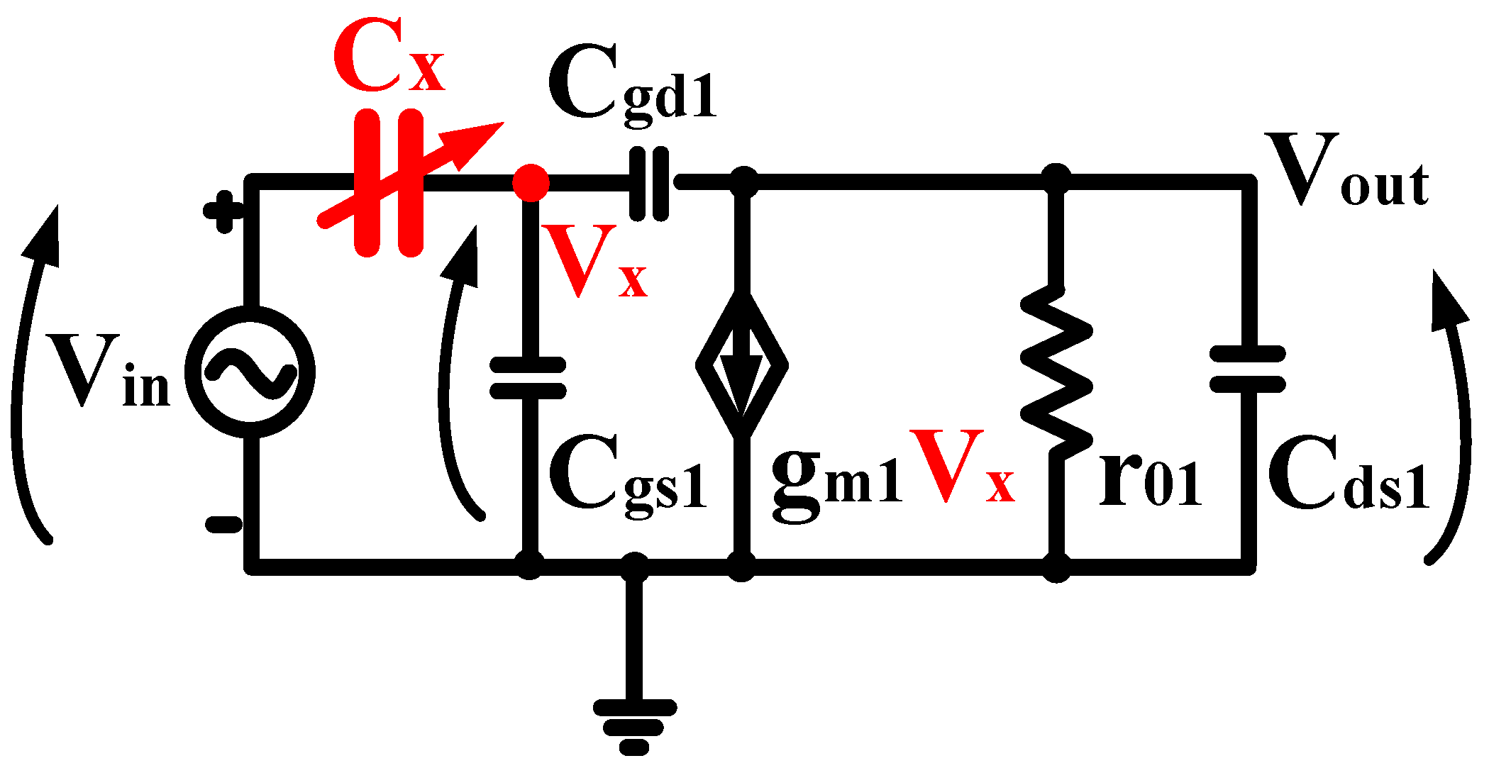
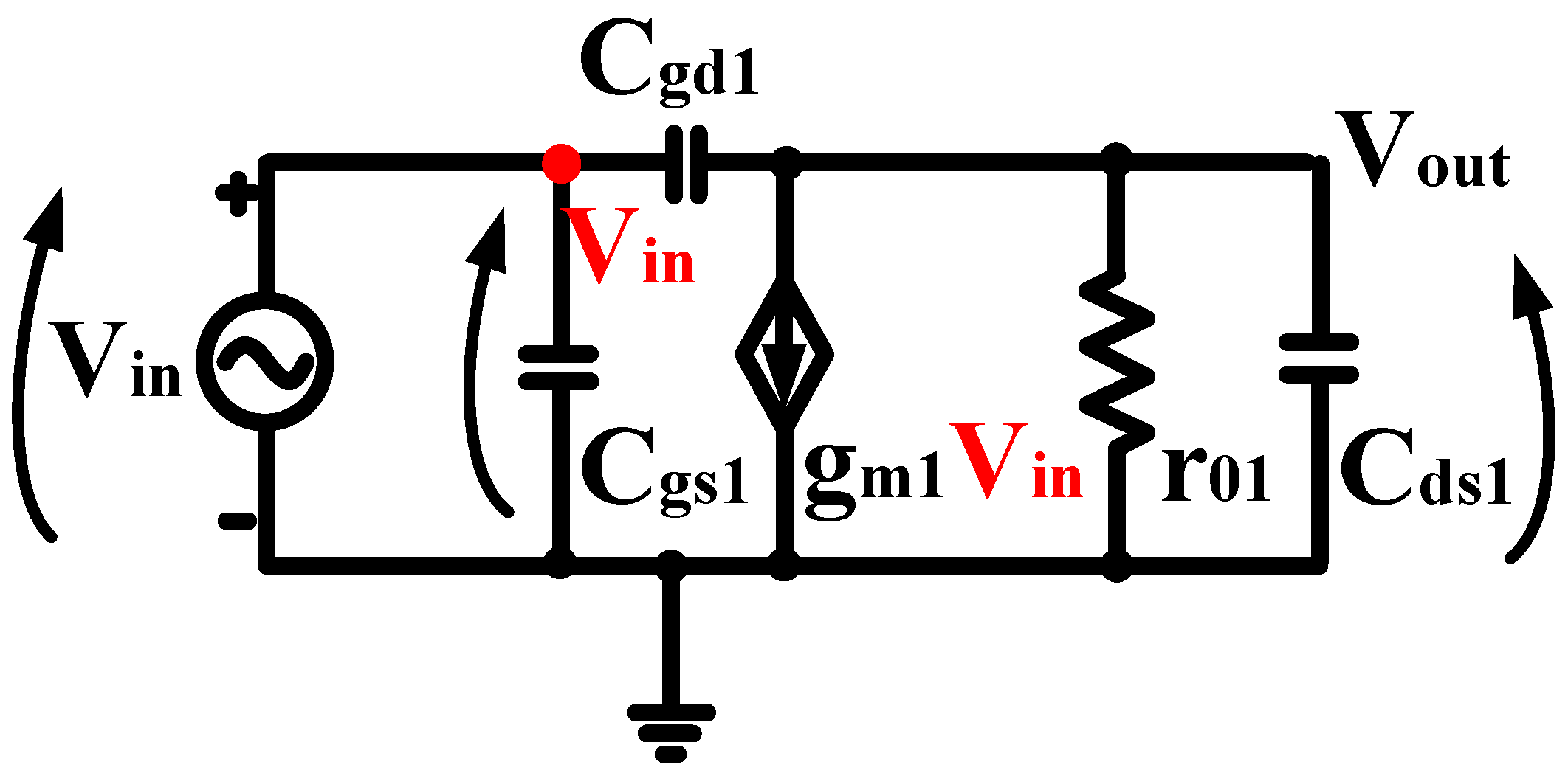
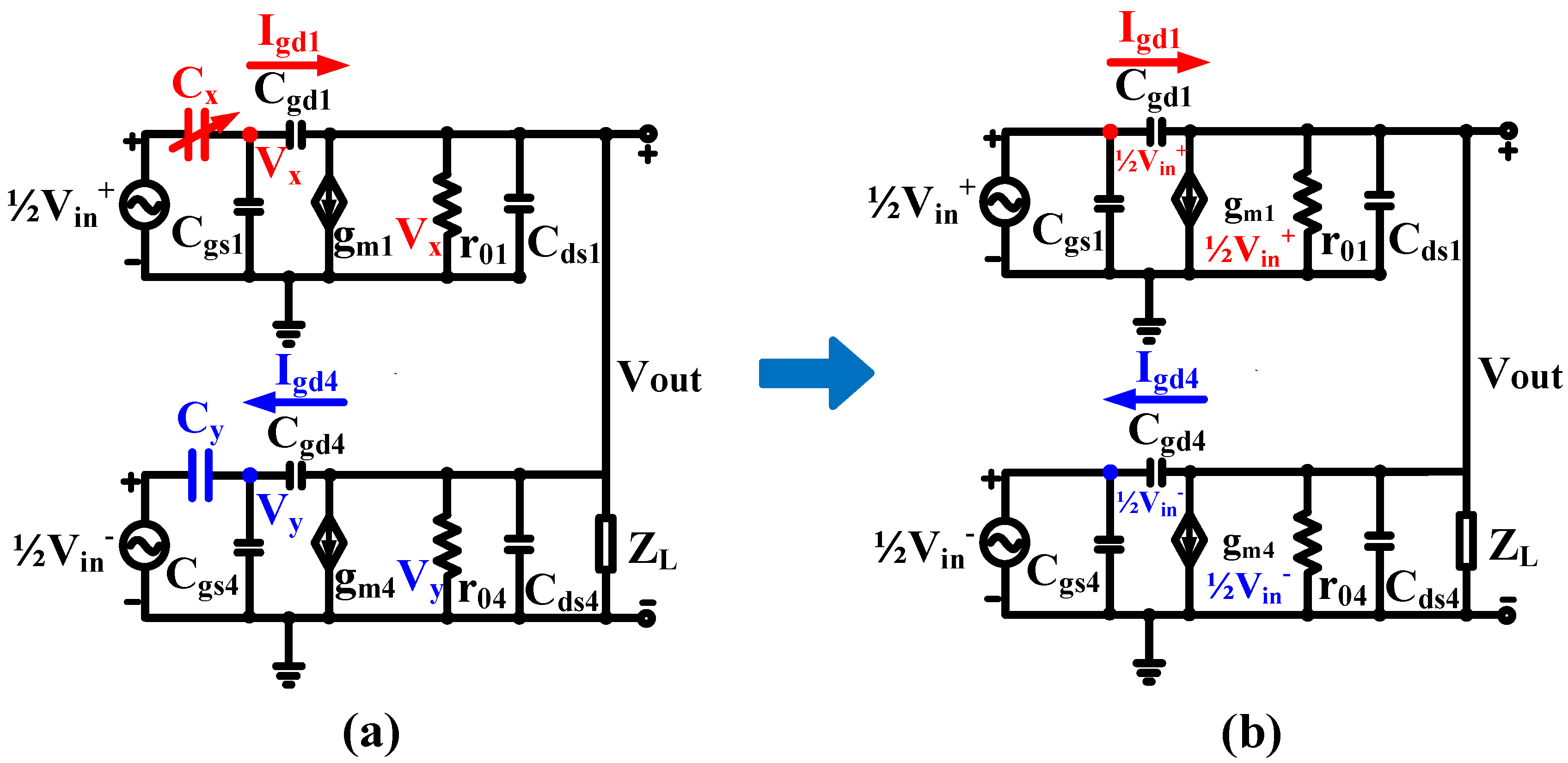
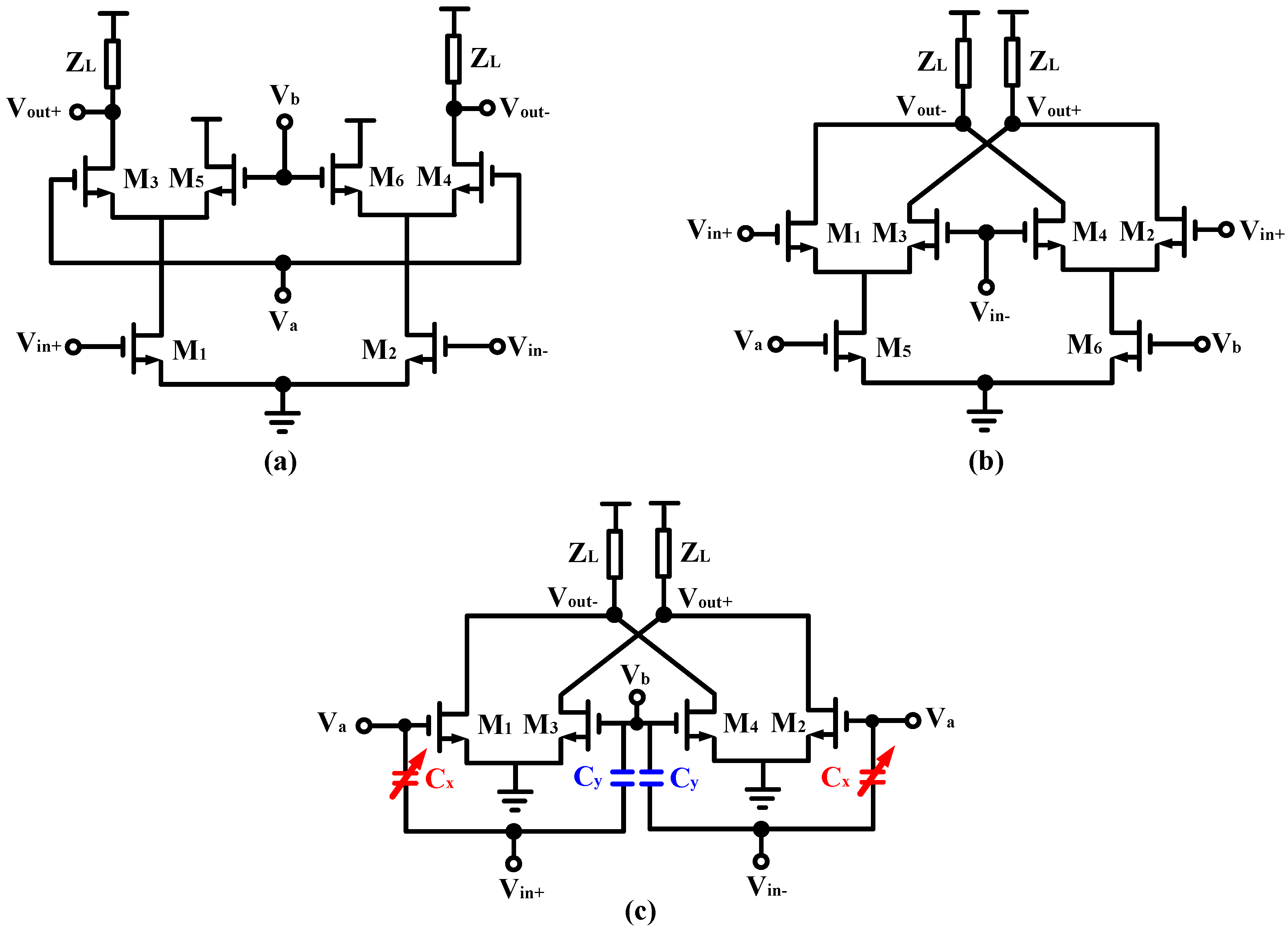
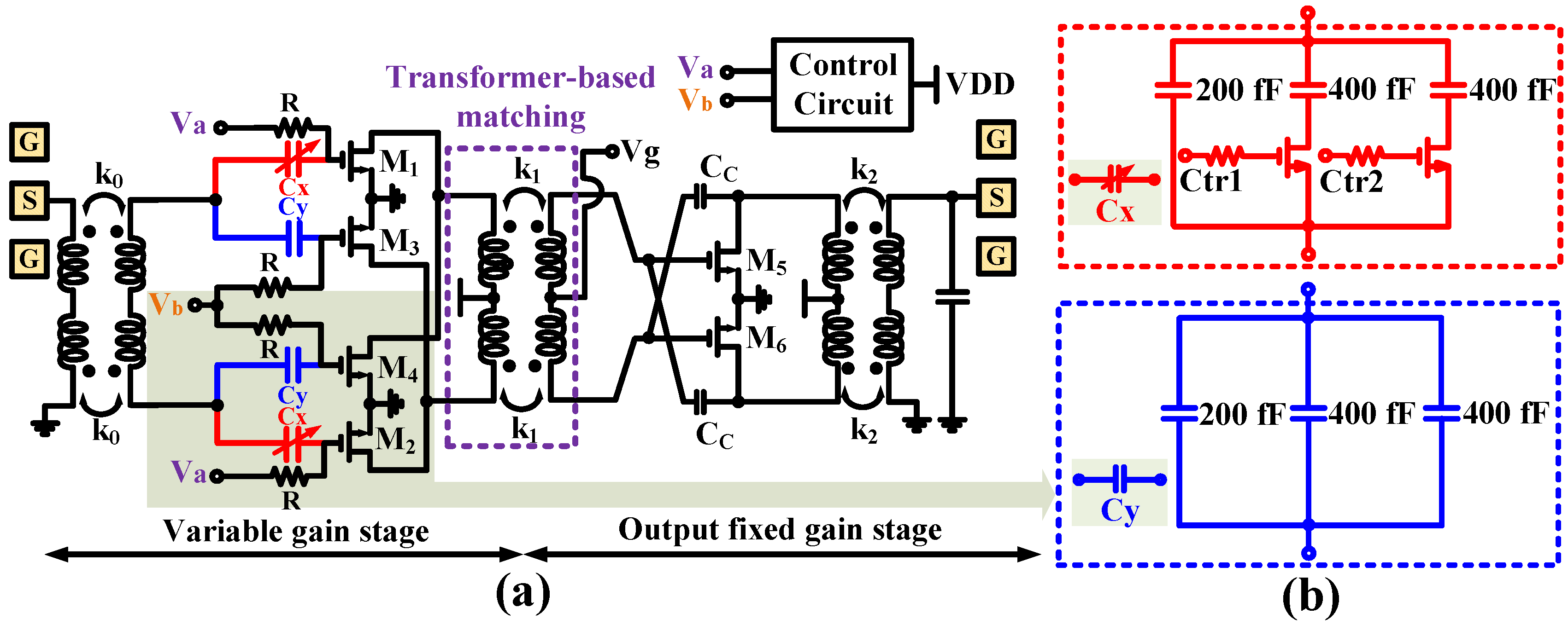
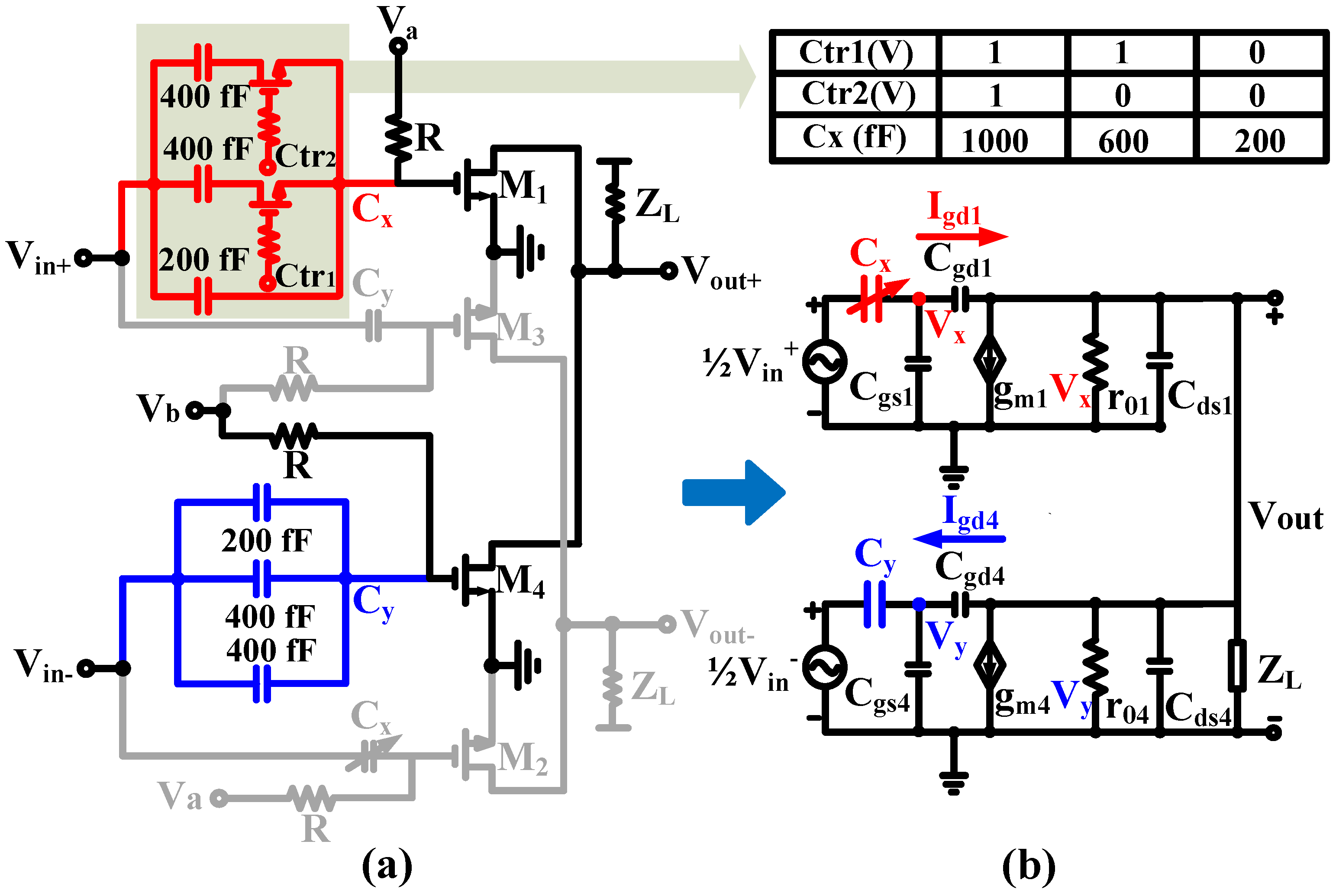
2.1. Asymmetric Capacitor-Based Reconfigurable Technique

The core idea behind the proposed asymmetric capacitor-based reconfigurable technique was to connect asymmetric capacitors Cx and Cy in series on the gate nodes of transistors (M1–M4), respectively, as shown in Figure 2a. It should be pointed out that since the value of Cx is different from Cy, it is called asymmetric capacitors. Adjusting the values of asymmetrical capacitors provides another dimension of gain control, and hence, reconfigurable gain tuning range and gain step can be achieved. Figure 2b depicts the structure of the applied asymmetric capacitors. To achieve three configurations, the adjustable capacitor Cx was designed to be composed of three capacitors and two switching transistors, which are controlled by the bias voltage of Ctr1 and Ctr2. In addition, to ensure the reconfigurable effect, it is necessary to ensure that the designed capacitances of the asymmetric capacitors are as close as possible to the desired theoretical value. Based on this, both of the asymmetric capacitors used in this study were metal insulator metal (MIM) topology, because of its high resistance to process deviation. Meanwhile, Cx and Cy used similar capacitor arrays.
To investigate the reconfigurable mechanism, the core of the variable gain stage is shown separately, and its simplified schematic diagram is shown in Figure 3a. For further and more intuitive theoretical analysis, the corresponding half-side small-signal equivalent circuit is also established, as shown in Figure 3b. Based on Figure 3b, the voltage gain can be calculated by
G = V o u t V i n + - V i n - A 1 g m 1 A 2 g m 4 ( 1 Z L + 1 r o 1 + 1 r o 4 + j ω C g d 1 + j ω C g d 4 + j ω C d s 1 + j ω C d s 4 )
where gm refers to the transconductances of transistors M1 and M4; the Cgd and Cds describe the parasitic gate-to-drain capacitor and drain-to-source capacitor, respectively; the ro represents channel output resistance; the ZL is used to characterize the load impedance. In addition, A1 and A2 are obtained by
A 1 = C x ( 1 r 01 + j ω C d s 1 + j ω C g d 1 ) ( C x + C g s 1 + C g d 1 ) ( 1 r 01 + j ω C d s 1 ) + ( C x + C g s 1 ) j ω C g d 1 + C g d 1 g m 1
A 2 = C y ( 1 r 04 + j ω C d s 4 + j ω C g d 4 ) ( C y + C g s 4 + C g d 4 ) ( 1 r 04 + j ω C d s 4 ) + ( C y + C g s 4 ) j ω C g d 4 + C g d 4 g m 4
where gm1 and gm4 are biased by Va and Vb, respectively, which are generated by a 7-bit DAC. According to (1), it can be observed that the voltage gain is proportional to the difference between Va and Vb; that is, the greater the difference between the two, the higher the gain. Based on this, to achieve the gain tuning of the VGA, Va should not be equal to Vb. Furthermore, when setting Va less than Vb, from (1), the maximum gain tuning range ΔGmax can be derived as
Δ G max = A 1 g m 1 , min -   A 2 g m 4 , max A 1 g m 1 , max -   A 2 g m 4 , min
where gm,min and gm,max are the transconductances of transistors biased in minimum and maximum control voltages. It should be pointed out that since the amplifier gain is in decibels, the voltage gain should be converted into decibels, after which the logarithmic operation is performed. Based on this, the normal difference operation becomes division when placed in the logarithmic operation. Therefore, the final derivation of the gain tuning range appears as a ratio. In addition, it is worth mentioning that the Cgd is not ignored but neutralized based on the proposed topology in deriving Equations (1)–(4). The detailed proofs of Equations(1)–(4) are presented in Appendix A.
Then, based on (4), the gain resolution Gr of the VGA can be calculated as
G r = Δ G max 2 n = 1 2 n ( A 1 g m 1 , min -   A 2 g m 4 , max ) ( A 1 g m 1 , max -   A 2 g m 4 , min )
where n is the control bits of the DAC. According to (4) and (5), the proposed asymmetric capacitor-based reconfigurable technique provides a new method to configure ΔGmax and Gr by adjusting the coefficients A1 and A2. Meanwhile, in order to keep the maximum gain of the VGA, it is needed to set A2 ≈ 1. As shown in Figure 4a,b, the conventional methods are only obtained ΔGmax and Gr by controlling transconductance gm of the transistors, whereas the proposed technique achieves another dimension for ΔGmax and Gr control. When A1 is varied from 1 to 0, ΔGmax and Gr will be reconfigured. When the asymmetric capacitors Cx and Cy are designed to be greater than 1000 fF across 20–30 GHz, it can be calculated from (2) and (3) that the values of the coefficients A1 and A2 are approximately equal to one. Conversely, when they are smaller than 1000 fF, the values of A1 and A2 will be less than one. Thus, the gain tuning range and gain step can be reconfigured, which is adjusted to capacitors Cx and Cy.
From what has been discussed above, the capacitance of Cx was adjusted by 2-bit switched-capacitor array, which could achieve 200/600/1000-fF; the Cy was designed to be a fixed value with a capacitance close to 1000 fF, so that the coefficient A2 was approximately equal to one, as shown in Figure 3a. By configuring different Cx values, the simulated small-signal gains versus frequency are plotted in Figure 4c. Among them, in order to observe the reconfigurable effect more intuitively, only the maximum and minimum gain states are shown in the results. At the minimum gain control mode, the gain of the VGA changes greatly as Cx increases from 200 fF to 1000 fF, while the gain is almost the same at the maximum gain control mode. As a result, the reconfigurable gain tuning range and gain step can be realized. The simulation results shown in Figure 4c agree well with the theoretical analysis.

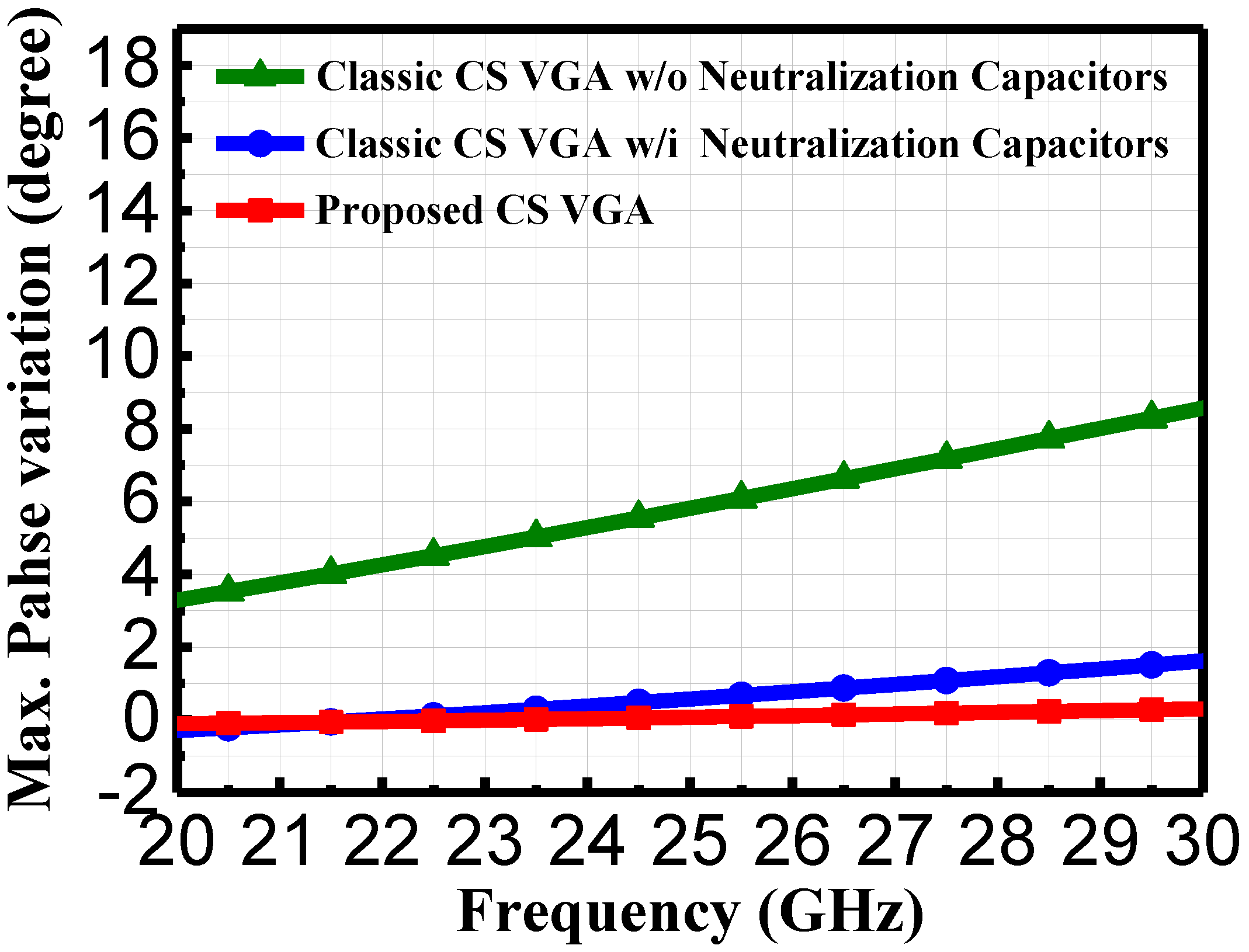
2.2. Phase Compensation Technique

For mm-wave VGAs, low additional phase shift during gain tuning is also a very important performance metric [9]. As mentioned before, many scholars have conducted extensive research to realize low phase variation during gain tuning. For VGAs with CS topologies, the parasitic capacitor Cgd has been discussed in detail [23] as the most important factor causing the phase variation. In order to eliminate Cgd, a method is widely used in amplifier design that introduces a positive feedback capacitor, which is called the capacitive cross-coupled neutralization (CCCN) technique [24]. This technique has the advantages of simple structure and obvious neutralization effect. However, its disadvantage is also obvious, that is, only good neutralization can be achieved in a narrow frequency band, as the positive feedback capacitor changes with frequency. This greatly limits the design of this technique in wideband VGA circuit design. To overcome this problem, the active neutralization technique in the previous study [23] was employed. The core idea of this technique is to replace the positive feedback capacitor in the conventional CCCN technique with an active transistor. Since the auxiliary transistors (M3 and M4) and the main transistors (M1 and M2) have the same size, the Cgd of the two can be guaranteed to be the same with frequency changes, thus achieving good neutralization in the wide frequency band.
Figure 5 plots the simulated maximum phase variation in the classic and proposed active neutralization-based CS VGAs across 20–30 GHz under the same gain adjustment range. Both simulations were conducted based on the same circuit configuration. Across 20–30 GHz, the maximum deviation of the phase variation in the proposed VGA with active neutralization technique was below 0.3° during gain tuning. In contrast, the maximum phase variation results for the two classic CS VGAs were relatively large. Among them, one VGA with conventional CCCN technique exhibited the maximum phase variation of 1.6°, while another VGA without any neutralization techniques showed 8.6° phase variation at 30 GHz. These results fully illustrate two points: (1) the proposed VGA with active neutralization technique can effectively eliminate Cgd and achieve low phase variation; (2) good phase compensation can be realized in the wide frequency band, which is very suitable for broadband VGA design.

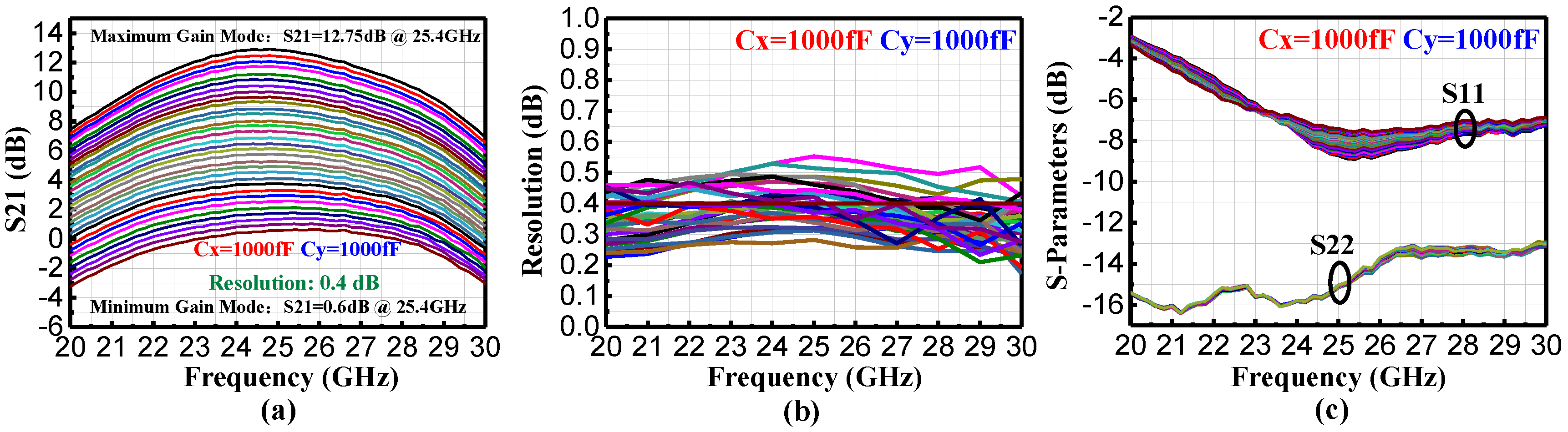
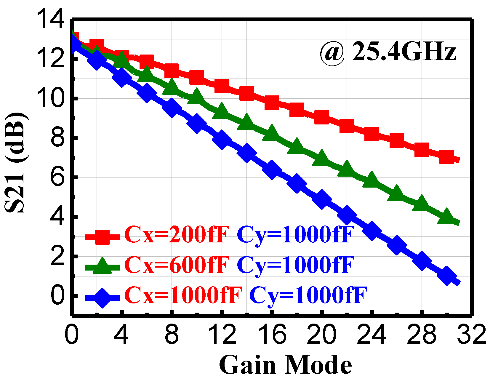
3. Measurement Results

The proposed reconfigurable digitally controlled CS VGA was fabricated in a 65 nm CMOS process, and its die micrograph is presented in Figure 6. In the case of not including PAD, the core area of this chip was 0.758 mm × 0.23 mm. The two-stage VGA had a total power consumption of 98 mW with a 1 V supply, and the selection of 1 V supply voltage followed the vendor’s recommendation under the corresponding process node. It is worth mentioning that, to achieve active neutralization, the auxiliary pairs in the proposed structure were on, which consumed slightly extra power to maintain the same gain. Even so, the total power consumption of the variable gain stage with the DAC was only 29 mW (including auxiliary pairs). The VGA presented in this paper consumed relatively high power consumption, which is because it achieved large output power. If a system does not need such high output power, the bias voltage of the output stage can be decreased, and the total dc power consumption of the proposed VGA would be reduced accordingly.
The VGA gain was controlled by Va and Vb, which were generated by the designed seven-bit DAC. The measured 32 states of gains under different control modes are shown in Figure 7a, Figure 8a and Figure 9a, respectively. It can be observed that the proposed VGA achieved a 12.2/9.2/6.1 dB gain tuning range, respectively, when the bias voltage of Ctr1 and Ctr2 were configured from 11 to 10 and then to 00 (Cx varying from 1000 to 200 fF, stepping 400 fF). Implementation of a 6.1 dB gain tuning range was aimed to insert loss compensation of PSs in phased array systems. Implementation of a 12.2 dB gain tuning range was intended for gain tuning in each element to suppress the sidelobes. As for the intermediate state, it was a compromise that was reserved according to actual design requirements. Meanwhile, the peak gain remained basically constant with the changes in Cx. The measured 3 dB bandwidth was as wide as 7.6 GHz, from 21.4 to 29 GHz, with an approximately 13 dB peak gain.
To further achieve the ultrahigh average sidelobe suppression ratio of the beamforming to ensure beamforming quality and chain data rate, the VGA was suggested to achieve a gain step of less than 0.5 dB [10]. As for insertion loss compensation of PSs, higher gain steps were also required, to avoid introducing extra gain errors. Based on the above considerations, the proposed VGA was designed to have a 0.4/0.3/0.2 dB gain resolution, respectively. Achieving such a high-precision gain step control, it was necessary to design a high-precision DAC. According to (5) and the measured gain tuning range, the calculation results of the three gain resolutions are as follows:
G r max = Δ G max 2 n = G max - G min 2 6 = 12.75 - 0.6 2 6 0.4
G r mean = Δ G max 2 n = G max - G min 2 6 = 12.9 3.7 2 6 0.3
G r min = Δ G max 2 n = G max - G min 2 6 = 13 6.9 2 6 0.2
Furthermore, the three configurations for the min, mean, and max gain step versus the six-bit binary control word overall frequency band are plotted in Figure 7b, Figure 8b and Figure 9b, respectively. The proposed VGA basically realized three reconfigurable gain steps of 0.4/0.3/0.2 dB, respectively. Then, the measured input return loss (S11) and output return loss (S22) of the VGA for the different configurations are plotted in Figure 7c, Figure 8c and Figure 9c, respectively. It can be seen from the results that changing the capacitance of Cx will slightly affect the offset of S11, which, due to the Cx, will slightly change the imaginary part of the source impedance. Since the output stage was a fixed gain stage, S22 basically remained unchanged versus 32 control words. In addition, it is worth mentioning that, to achieve wideband matching and compact layout, the transformer-based high-order matching networks were adopted. By adjusting the coupling coefficient k of the primary and secondary coils, the values of resonance frequency (ωL and ωH) could be adjusted, thereby realizing the adjustment of the bandwidth [25]. Figure 10 presents the measured small-signal gains versus 32 gain modes at 25.4 GHz, which verifies that the proposed VGA achieves reconfigurable gain tuning range and gain resolution, in addition to realizing linear gain control.
The RMS phase error was used to characterize the phase variation in the VGA. The specific formula for calculating RMS phase error is expressed as
R M S   P h a s e   E r r o r = 1 N i = 1 N | θ i - θ a v e | 2
where ϴi is the phase at the i state, and ϴave is the average of the phases of all states. In this paper, the phase was extracted from the argument of S21. The RMS phase errors for all gain states were measured by taking the maximum gain state as a reference, and they are shown in Figure 11a. At the maximum gain tuning range mode, the measured RMS phase error was 1.7° at 23.4 GHz. Across 20–30 GHz, the measured RMS phase error was less than 5.5°. At the medium gain tuning range mode (0.3 dB gain step), the measured minimum RMS phase error was 0.5° at 25.2 GHz. Across 20–30 GHz, the measured RMS phase error was less than 2.4°. At the finest gain step control condition, the RMS phase error measured across 20–30 GHz was lower than 1.9°. At 30 GHz, a minimum phase error of 0.22° was achieved. Meanwhile, under the maximum gain state, the OP1dB was up to 8.6 dBm at 25 GHz, as plotted in Figure 11b.
Table 1 summarizes the performance of this research and compares it to prior studies. The proposed VGA is the only one that can reconstruct gain tuning range and gain resolution, which will greatly increase the flexibility of phased array systems. Additionally, it is the only one that adopts stackless transistor topology, thus achieving the lowest supply voltage, compared with other state-of-the-art multiple-stack transistor structures.

4. Conclusions

A 21.4–29 GHz reconfigurable digitally controlled VGA based on stackless CS structure with novel asymmetric capacitor-based reconfigurable and active neutralization phase compensation techniques was introduced. The proposed VGA achieved a 12.2/9.2/6.1 dB gain tuning range with a 0.4/0.3/0.2 dB gain step while maintaining the peak gain constant. At the finest gain step mode, the measured RMS phase error was <1.9° across 20–30 GHz. At 30 GHz, a minimum phase error of 0.22° was achieved. At the maximum gain state, it achieved a measured 13 dB peak gain and 8.6 dBm OP1dB. The measurement characteristics demonstrate the proposed VGA is suitable for 5G mm-wave NR phased array beamformers that require reconfigurable gain tuning range and gain step with low phase variation.

Author Contributions

Conceptualization, Q.Z. and K.K.; methodology, Q.Z.; software, Q.Z.; validation, Q.Z., C.Z. and K.K.; formal analysis, Q.Z.; investigation, Q.Z.; resources, Q.Z.; data curation, Q.Z.; writing—original draft preparation, Q.Z.; writing—review and editing, Q.Z.; visualization, Q.Z.; supervision, K.K.; project administration, K.K.; funding acquisition, K.K. All authors have read and agreed to the published version of the manuscript.

Funding

This study is supported by the National Key R&D Program of China (2020YFB1805003, 2018YFB1802002), National Natural Science Foundation of China (Grant No. 61931007, 62025106).

Institutional Review Board Statement

Not applicable.

Informed Consent Statement

Not applicable.

Data Availability Statement

The study did not report any data.

Conflicts of Interest

The authors declare no conflict of interest.

Appendix A

Derivations of Equations (1)–(4)
Figure A1 shows a small-signal equivalent circuit of a common source (CS) amplifier with parasitic elements when the effect of asymmetric capacitors is considered.
Figure A1. Small-signal equivalent circuit with asymmetric capacitor Cx.
Electronics 11 00751 g0a1
According to Kirchhoff’s current law (KCL) and Kirchhoff’s voltage law (KVL), the following equations can be obtained:
{ ( V i n V x ) s C x = s C g s 1 V x + ( V x V o u t ) s C g d 1 ( V x V o u t ) s C g d 1 = g m 1 V x + ( 1 r o 1 + s C d s 1 ) V o u t
{ V i n s C x = s ( C x + C g s 1 + C g d 1 ) V x V o u t s C g d 1 V x ( s C g d 1 g m 1 ) = ( 1 r o 1 + s C d s 1 + s C d g 1 ) V o u t
V i n s C x = s ( C x + C g s 1 + C g d 1 ) 1 r 01 + s C g d 1 + s C d s 1 s C g d 1 g m 1 V o u t V o u t s C g d 1
V i n s C x ( s C g d 1 g m 1 ) = [ s ( C x + C g s 1 + C g d 1 ) ( 1 r 01 + s C d s 1 ) + s ( C x + C g s 1 + C g d 1 ) s C g d 1 s C g d 1 ( s C g d 1 g m 1 ) ] V o u t = [ s ( C x + C g s 1 + C g d 1 ) ( 1 r 01 + s C d s 1 ) + s ( C x + C g s 1 ) s C g d 1 + ( s C g d 1 ) 2 ( s C g d 1 ) 2 + s C g d 1 g m 1 ] V o u t = [ s ( C x + C g s 1 + C g d 1 ) ( 1 r 01 + s C d s 1 ) + s ( C x + C g s 1 ) s C g d 1 + s C g d 1 g m 1 ] V o u t
G a s y m m e t r i c = V o u t V i n = s C x ( s C g d 1 g m 1 ) s ( C x + C g s 1 + C g d 1 ) ( 1 r 01 + s C d s 1 ) + s ( C x + C g s 1 ) s C g d 1 + s C g d 1 g m 1 = C x ( s C g d 1 g m 1 ) ( C x + C g s 1 + C g d 1 ) ( 1 r 01 + s C d s 1 ) + ( C x + C g s 1 ) s C g d 1 + C g d 1 g m 1
Figure A2 shows the small-signal equivalent circuit of a CS amplifier with parasitic elements when the effect of asymmetric capacitors is not considered.
Figure A2. Small-signal equivalent circuit without asymmetric capacitor Cx.
Electronics 11 00751 g0a2
According to Kirchhoff’s current law (KCL) and Kirchhoff’s voltage law (KVL), it can be derived that
g m 1 V i n ( V i n V o u t ) s C g d 1 = V o u t r 01 V o u t C d s 1
In order to facilitate the operation, let Av = Vout/Vin. Then, Equation (A6) can be simplified to
g m 1 ( 1 A v ) s C g d 1 = A v r 01 A v s C d s 1
g m 1 r 01 s C g d 1 r 01 + A v s C g d 1 r 01 = A v A v s C d s 1 r 01
g m 1 r 01 s C g d 1 r 01 = A v A v s C d s 1 r 01 A v s C g d 1 r 01
g m 1 r 01 s C g d 1 r 01 = A v ( 1 + s C d s 1 r 01 + s C g d 1 r 01 )
A v = G s y m m e t r i c = V o u t V i n = j ω C g d 1 g m 1 ( 1 r o 1 + j ω C g d 1 + j ω C d s 1 )
In order to facilitate the operation, let:
A = jwCgd1gm1;
B = (Cx + Cgs1 + Cgd1)(1/ro1 + jwCds1) + (Cx + Cgs1)jwCgd1 + Cgd1gm1;
C = (1/ro1 + jwCgd1 + jwCds1).
Then, Equation (A5) can be simplified to
G a s y m m e t r i c = V o u t V i n = C x A B
Equation (A11) can be simplified to:
G s y m m e t r i c = V o u t V i n = A C
Based on Equations (A12) and (A13), A1 is given by
A 1 = G a s y m m e t r i c G s y m m e t r i c = C x A B ÷ A C = C x C B = C x ( 1 r 01 + j ω C d s 1 + j ω C g d 1 ) ( C x + C g s 1 + C g d 1 ) ( 1 r 01 + j ω C d s 1 ) + ( C x + C g s 1 ) j ω C g d 1 + C g d 1 g m 1
Similarly, A2 is given by
A 2 = C y ( 1 r 04 + j ω C d s 4 + j ω C g d 4 ) ( C y + C g s 4 + C g d 4 ) ( 1 r 04 + j ω C d s 4 ) + ( C y + C g s 4 ) j ω C g d 4 + C g d 4 g m 4
According to Equations (A14) and (A15), Equation (A5) can be written as
G a s y m m e t r i c = A 1 G s y m m e t r i c = A 1 ( j ω C g d 1 g m 1 ) ( 1 r o 1 + j ω C g d 1 + j ω C d s 1 )
Qualitatively analyzing Equation (A16), compared with the conventional symmetrical capacitor structure, the A1 coefficient is generated by the voltage divider of the asymmetrical capacitor Cx. Therefore, if the capacitance of Cx is large (equivalent to short-circuit without voltage divider), A1 is approximately equal to 1; on the contrary, if the capacitance of Cx is small, and there is a certain voltage divider, A1 will be less than 1.
Figure A3a shows the half-side small-signal equivalent circuit of the proposed variable gain stage with asymmetric capacitors. Since it is a half-side circuit, Vin becomes one-half. According to the above derivation, coefficients A1 and A2 are introduced due to the influence of the asymmetric capacitor. Therefore, in order to express the derivation of Equation (1) more clearly and concisely, we first use the symmetrical capacitor structure to derive Equation (1). Based on Equation (A16), for the asymmetric capacitor structure, coefficients A1 and A2 should simply be added later to the numerator. Figure A3b presents the half-side small-signal equivalent circuit of the variable gain stage without asymmetric capacitors. According to Kirchhoff’s current law (KCL) and Kirchhoff’s voltage law (KVL), it can be derived that
( 1 2 V i n + V o u t ) s C g d 1 = 1 2 g m 1 V i n + + V o u t ( 1 r 01 + s C d s 1 + 1 Z L + s C d s 4 + 1 r 04 ) + 1 2 g m 4 V i n - + ( V o u t 1 2 V i n - ) s C g d 4
1 2 V i n + ( s C g d 1 g m 1 ) + 1 2 V i n - ( s C g d 4 g m 4 ) = V o u t ( 1 r 01 + s C d s 1 + 1 Z L + s C d s 4 + 1 r 04 + s C g d 1 + s C g d 4 )
Since 1 2 V i n + = 1 2 V i n - , the left side of Equation (A18) can be simplified to Equations (A19) and (A20), respectively.
1 2 V i n + ( s C g d 1 g m 1 ) + 1 2 V i n + ( g m 4 s C g d 4 )
1 2 V i n ( s C g d 1 g m 1 ) + 1 2 V i n ( s C g d 4 g m 4 )
Since the two transistors are the same size, Cgd is the same (Cgd1 = Cgd4), the two Cgd values can cancel each other, and Equations (A19) and (A20) can be further simplified as
1 2 V i n + ( g m 1 g m 4 )
1 2 V i n ( g m 1 g m 4 )
Then, substituting Equation (A21) into Equation (A18) yields
1 2 V i n + ( g m 1 g m 4 ) = V o u t ( 1 r 01 + s C d s 1 + 1 Z L + s C d s 4 + 1 r 04 + s C g d 1 + s C g d 4 )
V i n + 2 V o u t = ( 1 r 01 + s C d s 1 + 1 Z L + s C d s 4 + 1 r 04 + s C g d 1 + s C g d 4 ) ( g m 1 g m 4 )
Similarly, substituting Equation (A22) into Equation (A18) yields
1 2 V i n ( g m 1 g m 4 ) = V o u t ( 1 r 01 + s C d s 1 + 1 Z L + s C d s 4 + 1 r 04 + s C g d 1 + s C g d 4 )
V i n - 2 V o u t = ( 1 r 01 + s C d s 1 + 1 Z L + s C d s 4 + 1 r 04 + s C g d 1 + s C g d 4 ) ( g m 1 g m 4 )
Then, Equations (A24)–(A26) are used to obtain
V i n + V i n - 2 V o u t = 2 ( 1 r 01 + s C d s 1 + 1 Z L + s C d s 4 + 1 r 04 + s C g d 1 + s C g d 4 ) ( g m 1 g m 4 )
Then, according to (A27), the voltage gain without asymmetric capacitors can be calculated by
G s y m m e t r i c = V o u t V i n + V i n - = ( g m 1 g m 4 ) ( 1 r 01 + s C d s 1 + 1 Z L + s C d s 4 + 1 r 04 + s C g d 1 + s C g d 4 )
Similarly, based on Equation (A16), when considering the asymmetric capacitors, coefficients A1 and A2 are simply added to the numerator, respectively, and Equation (A28) becomes
G a s y m m e t r i c = V o u t V i n + V i n - A 1 g m 1 A 2 g m 4 ( 1 Z L + 1 r o 1 + 1 r o 4 + j ω C g d 1 + j ω C g d 4 + j ω C d s 1 + j ω C d s 4 )
According to (A29), any voltage gain can be calculated by
G 1 = V o u t V i n + - V i n - = A 1 g m 1 , 1 A 2 g m 4 , 1 ( 1 Z L + 1 r o 1 + 1 r o 4 + j ω C g d 1 + j ω C g d 4 + j ω C d s 1 + j ω C d s 4 )
G 2 = V o u t V i n + - V i n - = A 1 g m 1 , 2 A 2 g m 4 , 2 ( 1 Z L + 1 r o 1 + 1 r o 4 + j ω C g d 1 + j ω C g d 4 + j ω C d s 1 + j ω C d s 4 )
Moreover, since the amplifier gain is in decibels, G1 and G2 need to be converted to decibels. Therefore, Equations (A30) and (A31) are modified as
G 1 ( d B ) = 20 lg ( V o u t V i n + - V i n - ) = 20 lg ( A 1 g m 1 , 1 A 2 g m 4 , 1 ( 1 Z L + 1 r o 1 + 1 r o 4 + j ω C g d 1 + j ω C g d 4 + j ω C d s 1 + j ω C d s 4 ) )
G 2 ( d B ) = 20 lg ( V o u t V i n + - V i n - ) = 20 lg ( A 1 g m 1 , 2 A 2 g m 4 , 2 ( 1 Z L + 1 r o 1 + 1 r o 4 + j ω C g d 1 + j ω C g d 4 + j ω C d s 1 + j ω C d s 4 ) )
Based on Equations (A32) and (A33), the gain tuning range ΔG can be derived as (G1(dB)−G2(dB)) as follows:
Δ G = G 1 ( d B ) G 2 ( d B ) = 20 lg ( ( A 1 g m 1 , 1 A 2 g m 4 , 1 ( 1 Z L + 1 r o 1 + 1 r o 4 + j ω C g d 1 + j ω C g d 4 + j ω C d s 1 + j ω C d s 4 ) ) ( A 1 g m 1 , 2 A 2 g m 4 , 2 ( 1 Z L + 1 r o 1 + 1 r o 4 + j ω C g d 1 + j ω C g d 4 + j ω C d s 1 + j ω C d s 4 ) ) ) = A 1 g m 1 , 1 -   A 2 g m 4 , 1 A 1 g m 1 , 2 -   A 2 g m 4 , 2
Figure A3. (a) Half-side small-signal equivalent circuit of the proposed variable gain stage with asymmetric capacitors; (b) half-side small-signal equivalent circuit of the proposed variable gain stage without asymmetric capacitors.
Electronics 11 00751 g0a3

References

  1. Huang, D.; Zhang, L.; Li, D.; Zhang, L.; Wang, Y.; Yu, Z. A 60-GHz 360° 5-Bit Phase Shifter with Constant IL Compensation Followed by a Normal Amplifier with ±1 dB Gain Variation and 0.6-dBm OP-1dB. IEEE Trans. Circuits Syst. II Express Briefs 2016, 64, 1437–1441. [Google Scholar] [CrossRef]
  2. Li, W.-T.; Chiang, Y.-C.; Tsai, J.-H.; Yang, H.-Y.; Cheng, J.-H.; Huang, T.-W. 60-GHz 5-bit Phase Shifter with Integrated VGA Phase-Error Compensation. IEEE Trans. Microw. Theory Tech. 2013, 61, 1224–1235. [Google Scholar] [CrossRef]
  3. Roh, W.; Seol, J.-Y.; Park, J.; Lee, B.; Lee, J.; Kim, Y.; Cho, J.; Cheun, K.; Aryanfar, F. Millimeter-wave beamforming as an enabling technology for 5G cellular communications: Theoretical feasibility and prototype results. IEEE Commun. Mag. 2014, 52, 106–113. [Google Scholar] [CrossRef]
  4. Chen, Z.; Jiang, Z.; Liu, Z.; Cheng, Y.; Zhang, L.; Chen, D.; Zhang, J.; Sun, S.; Dong, J.; Liu, P.; et al. A 256-QAM 39 GHz Dual-Channel Transceiver Chipset with LTCC Package for 5G Communication in 65 nm CMOS. In Proceedings of the 2018 IEEE/MTT-S International Microwave Symposium—IMS, Philadelphia, PA, USA, 10–15 June 2018; pp. 1476–1479. [Google Scholar]
  5. Gao, L.; Ma, Q.; Rebeiz, G.M. A 20–44-GHz Image-Rejection Receiver With >75-dB Image-Rejection Ratio in 22-nm CMOS FD-SOI for 5G Applications. IEEE Trans. Microw. Theory Tech. 2020, 68, 2823–2832. [Google Scholar] [CrossRef]
  6. Kibaroglu, K.; Sayginer, M.; Phelps, T.; Rebeiz, G.M. A 64-Element 28-GHz Phased-Array Transceiver With 52-dBm EIRP and 8–12-Gb/s 5G Link at 300 Meters Without Any Calibration. IEEE Trans. Microw. Theory Tech. 2018, 66, 5796–5811. [Google Scholar] [CrossRef]
  7. Pang, J.; Wu, R.; Wang, Y.; Dome, M.; Kato, H.; Huang, H.; Narayanan, A.T.; Liu, H.; Liu, B.; Nakamura, T.; et al. A 28-GHz CMOS Phased-Array Transceiver Based on LO Phase-Shifting Architecture With Gain Invariant Phase Tuning for 5G New Radio. IEEE J. Solid-State Circuits 2019, 54, 1228–1242. [Google Scholar] [CrossRef]
  8. Huang, M.-Y.; Wang, H. A Mm-Wave Wideband MIMO RX With Instinctual Array-Based Blocker/Signal Management for Ultralow-Latency Communication. IEEE J. Solid-State Circuits 2019, 54, 3553–3564. [Google Scholar] [CrossRef]
  9. Wang, Y.; Wu, R.; Pang, J.; You, D.; Fadila, A.A.; Saengchan, R.; Fu, X.; Matsumoto, D.; Nakamura, T.; Kubozoe, R.; et al. A 39-GHz 64-Element Phased-Array Transceiver with Built-In Phase and Amplitude Calibrations for Large-Array 5G NR in 65-nm CMOS. IEEE J. Solid-State Circuits 2020, 55, 1249–1269. [Google Scholar] [CrossRef]
  10. Zhao, D.; Gu, P.; Zhong, J.; Peng, N.; Yang, M.; Yi, Y.; Zhang, J.; He, P.; Chai, Y.; Chen, Z.; et al. Millimeter-Wave Integrated Phased Arrays. IEEE Trans. Circuits Syst. I Regul. Pap. 2021, 68, 3977–3990. [Google Scholar] [CrossRef]
  11. Shakib, S.; Elkholy, M.; Dunworth, J.; Aparin, V.; Entesari, K. 2.7 A wideband 28GHz power amplifier supporting 8 × 100 MHz carrier aggregation for 5G in 40 nm CMOS. In Proceedings of the 2017 IEEE International Solid-State Circuits Conference (ISSCC), San Francisco, CA, USA, 5–9 February 2017; pp. 44–45. [Google Scholar]
  12. Yi, Y.; Zhao, D.; You, X. A Ka-band CMOS Digital-Controlled Phase-Invariant Variable Gain Amplifier with 4-bit Tuning Range and 0.5-dB Resolution. In Proceedings of the 2018 IEEE Radio Frequency Integrated Circuits Symposium (RFIC), Philadelphia, PA, USA, 10–12 June 2018; pp. 152–155. [Google Scholar]
  13. Shin, G.; Kim, K.; Lee, K.; Jeong, H.-H.; Song, H.-J. An E-Band 21-dB Variable-Gain Amplifier with 0.5-V Supply in 40-nm CMOS. Electronics 2021, 10, 804. [Google Scholar] [CrossRef]
  14. Lee, S.; Park, J.; Hong, S. A Ka-Band Phase-Compensated Variable-Gain CMOS Low-Noise Amplifier. IEEE Microw. Wirel. Components Lett. 2019, 29, 131–133. [Google Scholar] [CrossRef]
  15. Gao, H.; Li, N.; Li, M.; Wang, S.; Zhang, Z.; Kuan, Y.-C.; Song, C.; Yu, X.; Gu, Q.J.; Xu, Z. A 6.5–12-GHz Balanced Variable-Gain Low-Noise Amplifier With Frequency-Selective Gain Equalization Technique. IEEE Trans. Microw. Theory Tech. 2021, 69, 732–744. [Google Scholar] [CrossRef]
  16. Kuo, C.-C.; Tsai, Z.-M.; Tsai, J.-H.; Wang, H. A 71–76 GHz CMOS variable gain amplifier using current steering technique. In Proceedings of the 2008 IEEE Radio Frequency Integrated Circuits Symposium, Atlanta, GA, USA, 15–17 June 2008; pp. 609–612. [Google Scholar]
  17. Hsieh, C.-Y.; Kao, J.-C.; Kuo, J.-J.; Lin, K.-Y. A 57–64 GHz low-phase-variation variable-gain amplifier. In Proceedings of the 2012 IEEE/MTT-S International Microwave Symposium Digest, Montreal, QC, Canada, 17–22 June 2012; pp. 1–3. [Google Scholar]
  18. Siao, D.-S.; Kao, J.-C.; Wang, H. A 60 GHz Low Phase Variation Variable Gain Amplifier in 65 nm CMOS. IEEE Microw. Wirel. Components Lett. 2014, 24, 457–459. [Google Scholar] [CrossRef]
  19. Kong, L.; Chen, Y.; Boon, C.C.; Mak, P.; Martins, R.P. A Wideband Inductorless dB-Linear Automatic Gain Control Amplifier Using a Single-Branch Negative Exponential Generator for Wireline Applications. IEEE Trans. Circuits Syst. I Regul. Pap. 2018, 65, 3196–3206. [Google Scholar] [CrossRef]
  20. Huang, D.; Zhang, L.; Zhang, L.; Wang, Y. A 60-GHz, 15-dB Gain Range Digitally Controlled Phase-Inverting VGA With 0-dBm OP1 dB and 3° Phase Variation in 65-nm CMOS. IEEE Microw. Wirel. Compon. Lett. 2018, 28, 819–821. [Google Scholar] [CrossRef]
  21. Kim, S.H.; Jang, T.H.; Kim, J.H.; Park, C.S. A Wideband 120-GHz Variable Gain Amplifier with Multistage Phase Compensation. IEEE Trans. Microw. Theory Tech. 2020, 68, 2419–2427. [Google Scholar] [CrossRef]
  22. Park, J.; Lee, S.; Lee, D.; Hong, S. 9.8 A 28GHz 20.3%-Transmitter-Efficiency 1.5°-Phase-Error Beamforming Front-End IC with Embedded Switches and Dual-Vector Variable-Gain Phase Shifters. In Proceedings of the 2019 IEEE International Solid-State Circuits Conference (ISSCC), San Francisco, CA, USA, 17–21 February 2019; pp. 176–178. [Google Scholar]
  23. Wu, T.; Zhao, C.; Liu, H.; Wu, Y.; Yu, Y.; Kang, K. A 20~43 GHz VGA with 21.5 dB Gain Tuning Range and Low Phase Variation for 5G Communications in 65-nm CMOS. In Proceedings of the 2019 IEEE Radio Frequency Integrated Circuits Symposium (RFIC), Boston, MA, USA, 2–4 June 2019; pp. 71–74. [Google Scholar]
  24. Chan, W.L.; Long, J.R. A 58–65 GHz Neutralized CMOS Power Amplifier With PAE Above 10% at 1-V Supply. IEEE J. Solid-State Circuits 2010, 45, 554–564. [Google Scholar] [CrossRef]
  25. Li, C.-H.; Liu, Y.-L.; Kuo, C.-N. A 0.6-V 0.33-mW 5.5-GHz receiver front-end using resonator coupling technique. IEEE Trans. Microw. Theory Tech. 2011, 46, 1629–1638. [Google Scholar] [CrossRef]
Figure 1. Commonly used mm-wave VGA structures: (a) classic current-steering VGA with two-stack transistor structure; (b) classic Gilbert-cell-based VGA with two-stack transistor structure; (c) proposed CS VGA with stackless transistor structure.
Electronics 11 00751 g001
Figure 2. (a) Schematic of the proposed reconfigurable digitally controlled VGA and (b) diagram of the structure of the asymmetric capacitors Cx and Cy, where Cx is an adjustable capacitor and Cy is a fixed capacitor.
Electronics 11 00751 g002
Figure 3. (a) Simplified schematic of the proposed variable gain stage and (b) its half-side small-signal equivalent circuit.
Electronics 11 00751 g003
Figure 4. (a) Conventional methods to obtain ΔGmax and Gr; (b) a new method to configure ΔGmax and Gr with proposed asymmetric capacitor-based reconfigurable technique; (c) with different values of Cx, simulated small-signal gain versus frequency at the maximum and minimum control states.
Electronics 11 00751 g004
Figure 5. Simulated maximum phase variation in the classic CS VGAs and the proposed active neutralization-based CS VGA across 20–30 GHz under the same gain adjustment range.
Electronics 11 00751 g005
Figure 6. Micrograph of the proposed VGA.
Electronics 11 00751 g006
Figure 7. Based on Cx = 1000 fF, Cy = 1000 fF (Ctr1 = 1 V, Ctr2 = 1 V): (a) measured 32 gain states versus frequency and (b) its corresponding 31 gain resolutions versus frequency; (c) measured S11 and S22 versus frequency at 32 control states.
Electronics 11 00751 g007
Figure 8. Based on Cx = 600 fF, Cy = 1000 fF (Ctr1 = 1 V, Ctr2 = 0 V): (a) measured 32 gain states versus frequency and (b) its corresponding 31 gain resolutions versus frequency; (c) measured S11 and S22 versus frequency at 32 control states.
Electronics 11 00751 g008
Figure 9. Based on Cx = 200 fF, Cy = 1000 fF (Ctr1 = 0 V, Ctr2 = 0 V): (a) measured 32 gain states versus frequency and (b) its corresponding 31 gain resolutions versus frequency; (c) measured S11 and S22 versus frequency at 32 control states.
Electronics 11 00751 g009
Figure 10. Measured gains versus gain mode under different control modes at 25.4 GHz.
Electronics 11 00751 g010
Figure 11. (a) Measured RMS phase errors versus frequency at different control modes; (b) measured large signal performance of the VGA at 25 GHz.
Electronics 11 00751 g011
Table 1. Performance summary and comparison of the VGAs.
This StudyISSCC
2017 [11]
RFIC
2018 [12]
MWCL
2019 [14]
TMTT
2021 [15]
Technology65 nm
CMOS
40 nm
CMOS
65 nm
CMOS
65 nm
CMOS
55 nm
CMOS
TopologyStacklessTwo-stackTwo-stackTwo-stackTwo-stack
Supply (V)11.11.21.21.3
Freq (GHz)21.4–2926–3627–4230–34.56.5–12
S11 (dB)−9~−5−20~−10−30~−4−28~−11−14~−36
S22 (dB)−17~−13−7~−6−50~−5−30~−10−14~−35
Peak gain (dB)1322.49.620.820.7
ΔG (dB)12.2/9.2/6.187.510.618
Gain resolution (dB)0.4/0.3/0.210.520.1N/A
RMS phase error (°)<1.9/2.4/5.5<6 *<3.5<8 **<4.5
OP1 dB (dBm)8.613.72.5−0.6 #7.5 #
PDC (mW)9830.315.626.775
Core Area (mm2)0.1740.230.0830.20.98
* Estimated from measurement results; ** phase variation; # calculated from IP1dB with gain.
Publisher’s Note: MDPI stays neutral with regard to jurisdictional claims in published maps and institutional affiliations.

