Abstract
Recently, due to their abundant benefits, current-mode instrumentation amplifiers have received considerable attention in medical instrumentation and read-out circuit for biosensors. This paper is focused on the design of current-mode instrumentation amplifiers for portable, implantable, and wearable electrocardiography and electroencephalography applications. To this end, a CMOS differential voltage second-generation current conveyor (DVCCII) based on a linear transconductor is presented. A new band-pass instrumentation amplifier, based on the designed DVCCII, is also implemented in this paper. The concept of the proposed differential voltage current conveyor and instrumentation amplifier is validated numerically and their predicted performance is presented. The simulation results of the presented circuits were tested for 0.18 μm TSMC CMOS technology in a post layout simulation level using the Cadence Virtuoso tool with a ±0.9 V power supply, and demonstrated that the designed DVCCII has a wide dynamic range of ±400 mV and ±0.85 mA and a power consumption of 148 μW. The layout of the DVCCII circuit occupies a total area of 0.378 μm2. It is shown that the designed DVCCII benefits from good linearity over a wide range of input signals and provides a low input impedance at terminal X. Two versions of the proposed band-pass instrumentation amplifier using pseudo resistances were designed with different specifications for two different applications, namely for EEG and ECG signals. Numerical analyses of both designs show proper outputs and frequency responses by eliminating the undesired artifact and DC component of the EEG and ECG input signals.
1. Introduction
Cardiovascular diseases and strokes remain the two biggest causes of death worldwide [1,2]. Thus, monitoring and recording electrocardiogram (ECG) and electroencephalogram (EEG), bio-potential signals from the heart and brain of patients, are essential in the analysis of various physiological parameters and diagnosis [3,4]. An effective method for monitoring these signals while patients are moving around to do their daily activities is to utilize non-invasive, wearable, and implantable systems [1,3,4,5,6,7,8].
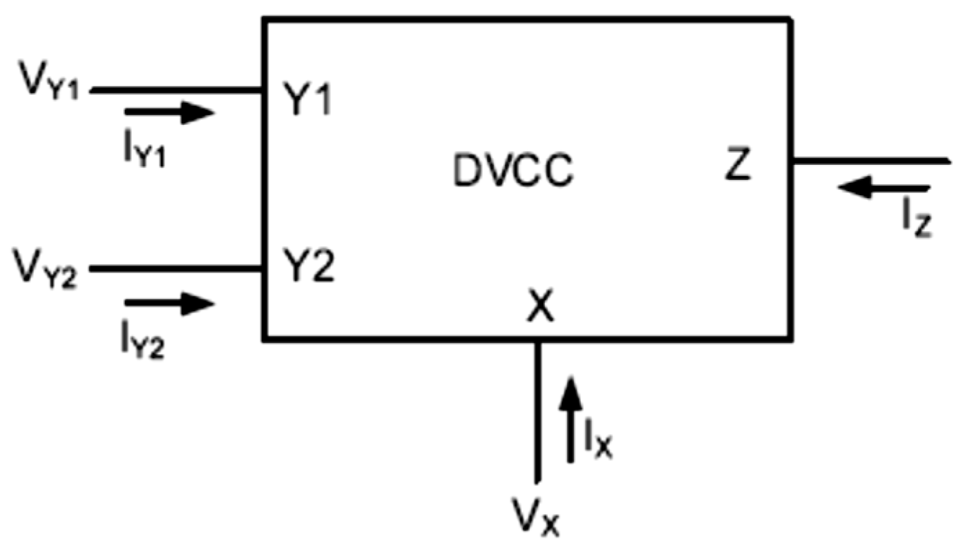
Among various types of medical instrumentation and read-out circuits for biosignals, current-mode integrated circuits have recently gained considerable attention due to their numerous benefits, such as large bandwidth, wide dynamic range, high linearity, low power consumption, and simple circuitry. Therefore, various types of current conveyors are the most widely used current-mode active building blocks [9,10,11,12,13,14]. The second-generation current conveyor (CCII), one of the most versatile current mode building blocks, was introduced by Sedra and Smith in 1970 [15]. The CCII has proved to be an efficient building block for application in numerous high frequency analog circuits, such as filters [6,15,16,17,18,19,20] and current-mode oscillators [21,22]. Recently, it has also been used in biomedical applications, such as instrumentation amplifiers [11,23,24,25]. One limitation of CCII is that the circuit has only one high-impedance terminal, which is not suitable for applications, such as the impedance converter or differential current-mode amplifiers where two high-impedance terminals are required. In order to address this limitation, the concept of a differential voltage current conveyor (DVCC) is proposed in [26,27]. As shown in Figure 1, a DVCC device is a four-terminal circuit, which has one low impedance input terminal X, two high-impedance input terminals Y1 and Y2, and one high-impedance output node Z.

Figure 1.
Differential voltage CCII block diagram.
The relation between the voltages and currents of the terminals is given by the following matrix:
where,
VX = VY1 − VY2, IZ = IX
The differential voltage between two input terminals, Y1 and Y2, appears at the terminal X, and the current injected into terminal X is being replicated to the output terminal Z. Thus, in an ideal DVCC the input resistance at terminal X is zero, and the resistance at terminal Z and both Y terminals is infinity. Therefore, a current flowing through Y1 and Y2 terminals is ideally zero. In practice, however, the input resistances and currents in DVCCs are different from the ideal case. Another desirable characteristic is the linearity of the device.
To address these issues, in this paper, a new design of a DVCCII with good linearity and low input and output impedance is presented. In addition, in the following, an instrumentation amplifier based on the designed DVCCII is presented. Instrumentation amplifiers (IAs) have found many applications in medical instrumentation: the read-out circuit of biosensors, electrocardiography, data acquisition, etc. [8,28,29,30,31,32,33]. To extract the low-value differential signals in the presence of large-value unwanted common-mode signals and noise, IAs with a high common-mode rejection ratio (CMRR) are required. For many years, voltage-mode instrumentation amplifiers (VMIAs) with three operational amplifiers (op-amps) and seven resistors were used for this purpose [8,34]. These circuits suffer from high power consumption due to the use of three op-amps and resistors, relatively complicated circuits, and limited bandwidth (BW). In addition, they require precise resistor matching to achieve high CMRR. After the introduction of the current-mode design to solve major problems associated with conventional VM, CM instrumentation amplifiers received considerable attention [11,32]. Instead of VM op-amps, CM building blocks, such as second-generation current conveyors (CCIIs), operational floating current conveyors (OFCC), differential voltage current conveyors (DVCCs), etc., are employed to design a new class of instrumentation amplifiers [11]. Compared with conventional VMIAs, CMIAs do not require matched resistors to provide a high CMRR. They also offer the extended differential mode gain independent of bandwidth [11,25,32].
Moreso, note that in the context of EEG and ECG signals, wideband performance is not required. Therefore, this study has been focused on the application of CMIAs to benefit from other advantages of current-mode amplifiers, such as a simpler circuitry, smaller on-chip area, low power consumption, and higher linearity. These are important features, especially in portable devices such as implantable and wearable biomedical microsystems, where the size and avoiding passive off-chip elements, weight, and power consumption—due to the limitation of battery usage—are critical issues. This study was not aimed at achieving a wide bandwidth, however, this feature has been achieved as a byproduct.
The structure of the paper is as follows. The proposed DVCC circuit is presented and discussed in the next section. In order to validate the DVCC design, simulation results using CAD tools in a post layout level and the realization of a DVCC-based instrumentation amplifier are also provided in the methods section. The applications of the proposed instrumentation amplifier for ECG and EEG signal filtering and amplification are presented in the results section. Finally, the achievements of the study are highlighted in the conclusion.
2. Methods
2.1. DVCCII Circuit
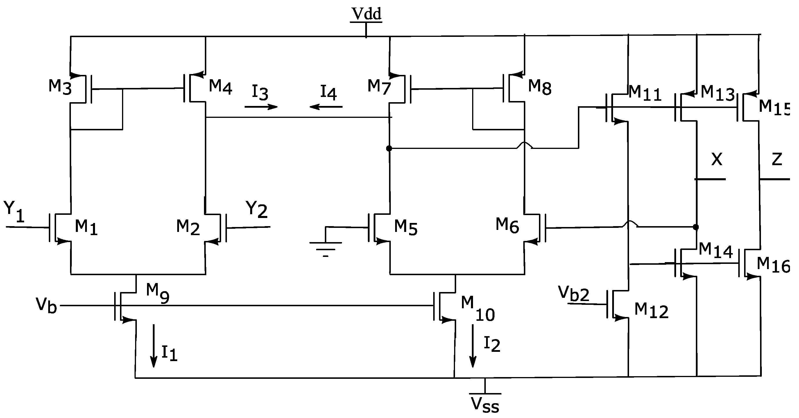
The schematic of the designed DVCCII, which is based on two wide linear range transconductor stages, is depicted in Figure 2. The pair of transconductors are formed by transistors M1 to M10. These two stages should have equal output currents. The voltage follower stage is connected to the outputs of these two identical transconductors, such that the I3 and I4 currents are equal in magnitude. Thus:
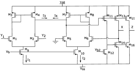
Figure 2.
CMOS realization of the designed DVCC. The differential voltage between two input terminals, Y1 and Y2, appears at the X terminal and the current injected at X terminal is being replicated to the output.
Using this configuration, since the transconductor stages are identical (with the same transistor sizing) and one of the inputs of the second transconductor (gate of M3) is grounded, the voltage at terminal X follows the voltage difference of the terminals Y1 and Y2. Note that this is valid, as long as both output currents are linear and M1–M4 are in saturation.
The output stage is formed by a Class-AB CMOS push–pull network that guarantees high current driving capability and low standby current. The current at terminal X is transferred to terminal Z through transistors M15 and M16. Thus, for achieving unit current gain, M15 and M16 must be matched with M13 and M14, respectively. All transistors are sized to operate in the saturation region. The size of the transistors is listed in Table 1.

Table 1.
Transistor sizing of the designed DVCC.
2.2. Post Layout Simulation Results
In order to validate the proposed DVCC, it was simulated using Cadence. TSMC 0.18 μm standard CMOS technology was used for the simulation. Transistor sizes that were used in the simulation correspond to those listed in Table 1. The utilized power supply was ±0.9 V.
Since the ports X and Z have unity current gains, in order to calculate the currents Ix and Iz to depict the curve, both ports are terminated with 5 KΩ resistances. Moreso, note that port X is an output voltage port that has a small output resistance. Therefore, it should be loaded with a relatively large resistor. A 5 KΩ resistor seems to be large enough for this purpose.
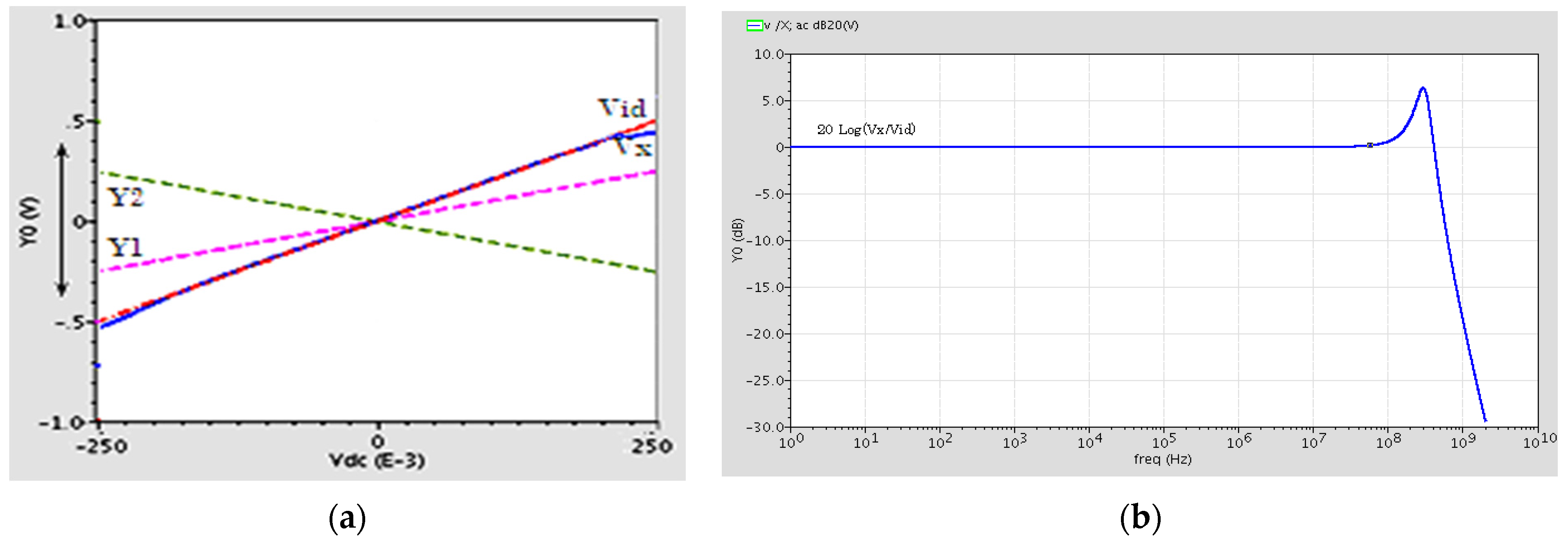
In order to investigate the linearity of the proposed circuit, the variations of the output voltage at terminal X versus variations in Vid = VY1 − VY2 are depicted in Figure 3a. The figure shows good linearity for differential input voltages between ±0.4 V. The offset voltage is also measured 2.24 mV and it is small enough. The offset voltage is the voltage of terminal X when Vid is equal to zero or is grounded.
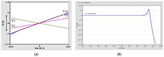
Figure 3.
(a) The X terminal output voltage versus changes of Vid. (b) Frequency response of the DVCC.
Figure 3b shows the voltage frequency response of the DVCC. It shows a flat response with a unity voltage gain (Vx/Vid) of 80 MHz and a 3 dB bandwidth of 450 MHz.
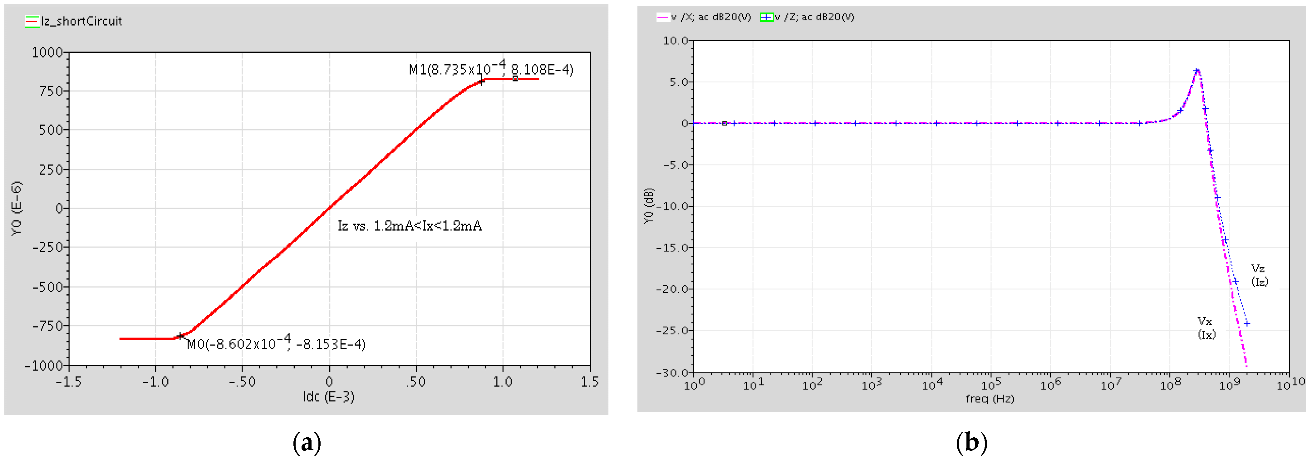
The output current at terminal Z versus the input current at terminal X, when terminal Z is shorted and the Ix current source is injected into terminal X, is shown in Figure 4a. The figure shows a ±0.85 mA linear range. Figure 4b shows the current frequency response of the DVCC. As seen, this DVCC has a good flat Iz/Ix response with a unity gain up to about 80 MHz and its 3 dB bandwidth is equal to 450 MHz.
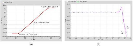
Figure 4.
(a) Output current of terminal Z versus terminal X input current, when terminal Z is shorted. (b) Current frequency response (Iz/Ix) of the DVCC.
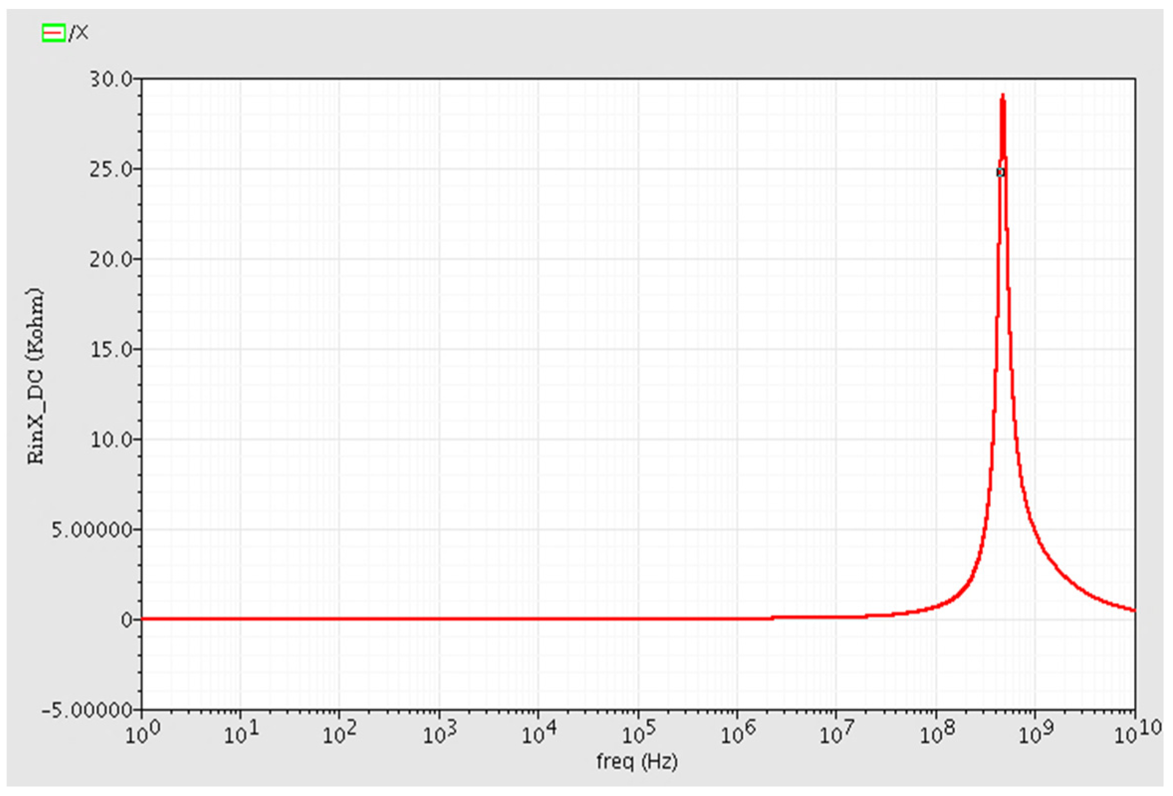
The simulated input impedance of terminal X, i.e., RX, is smaller than 20 ohm at DC and low frequencies. Variations of Rx versus frequency is depicted in Figure 5. The value of Rx is also lower than 1 KΩ up to 3 dB frequency, demonstrating that port X can operate as a low impedance output port.
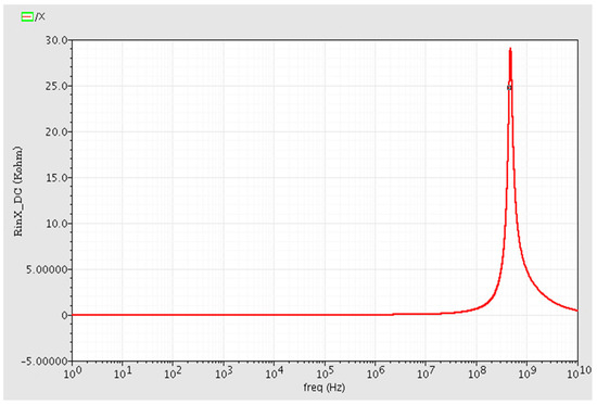
Figure 5.
The X terminal input resistance RX versus frequency changes. It is measured less than 20 ohm in low frequency and DC operation regions.
All results are summarized in Table 2. The table shows this design has proper characteristics for a DVCC.

Table 2.
Simulation results of designed DVCCII.
The layout of the proposed DVCCII using the Cadence tool with TSMC 0.18 μm standard CMOS technology is depicted in Figure 6. The on-chip area with this layout is estimated to be equal to 378 µm2.
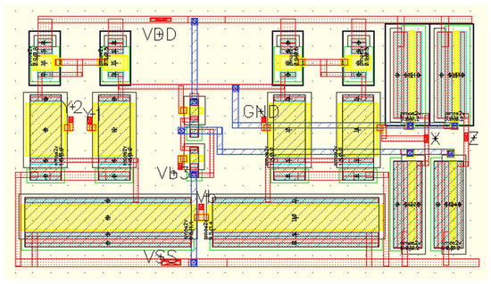
Figure 6.
The layout of the proposed DVCCII using Cadence with TSMC 0.18 μm standard CMOS technology.
It is worth mentioning, that by decreasing the supply and bias voltages, the linear dynamic range of the output voltage is restricted to ±0.3 V, and the frequency band of flat response with a unity voltage gain is reduced to about 38 MHz, but, consequently, the power consumption will be reduced to about 39 µW.
2.3. Design of DVCC-Based Instrumentation Amplifier
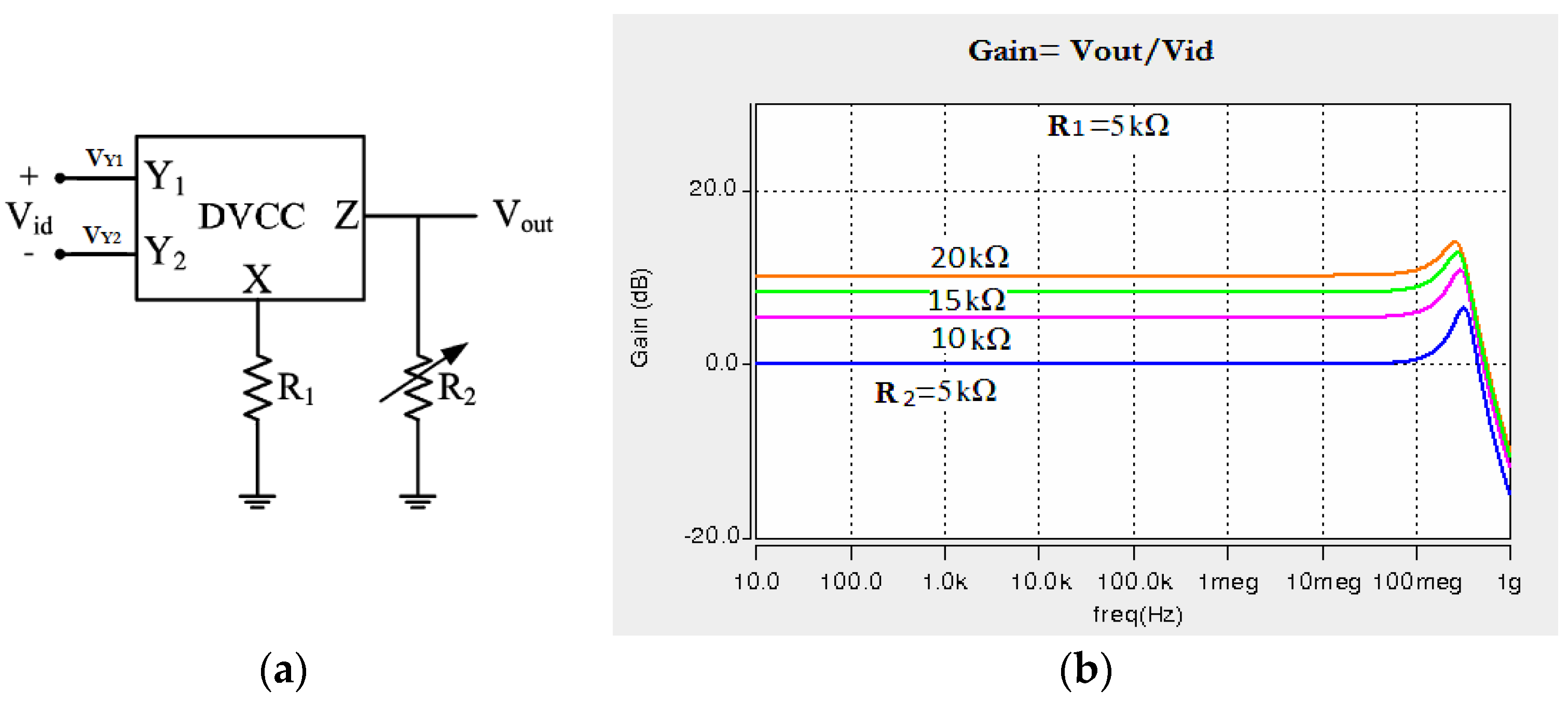
This section is devoted to the design of an instrumentation amplifier using the presented DVCC and its application in the amplification and filtering of low frequency biomedical signals. The block diagram and related voltage gains of the circuit for different values of resistance R2 are depicted in Figure 7. The gain of the instrumentation amplifier is given by .

Figure 7.
(a) The block diagram of the instrumentation amplifier implemented using the presented DVCC, (b) Voltage gains for different resistances at the output of this instrumentation amplifier.
Features of the designed CMIA are presented in Table 3. The table also highlights the advantages of the proposed amplifier in terms of power consumption, on-chip area, bandwidth, etc., compared to other studies.
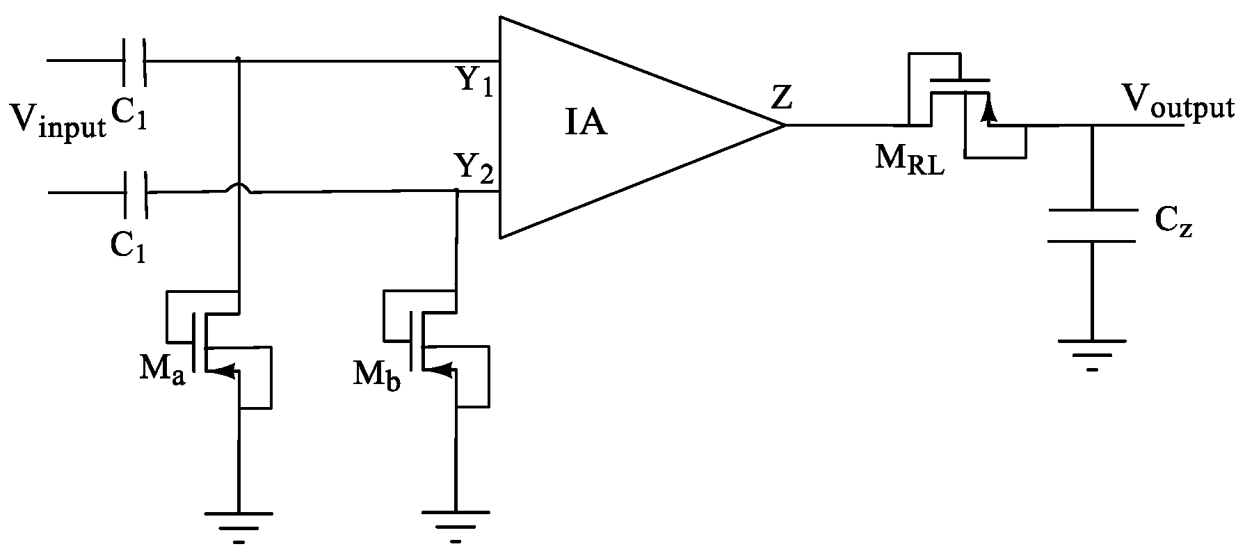
Moreso, note that the designed CMIA also benefits from a large BW as a byproduct. To limit the bandwidth to the required frequency band, we then used a filter. The proposed configuration for filtering specified frequency bands, which leads to forming a band-pass instrumentation amplifier, is shown in Figure 8. However, note that in addition to the application in EEG/ECG recordings, the designed DVCC and CMIA are general designs that can be used for many applications with a wide BW up to 450 MHz.

Figure 8.
The schematic of the proposed configuration for separating the required frequency bands for various biomedical signals through the IA.
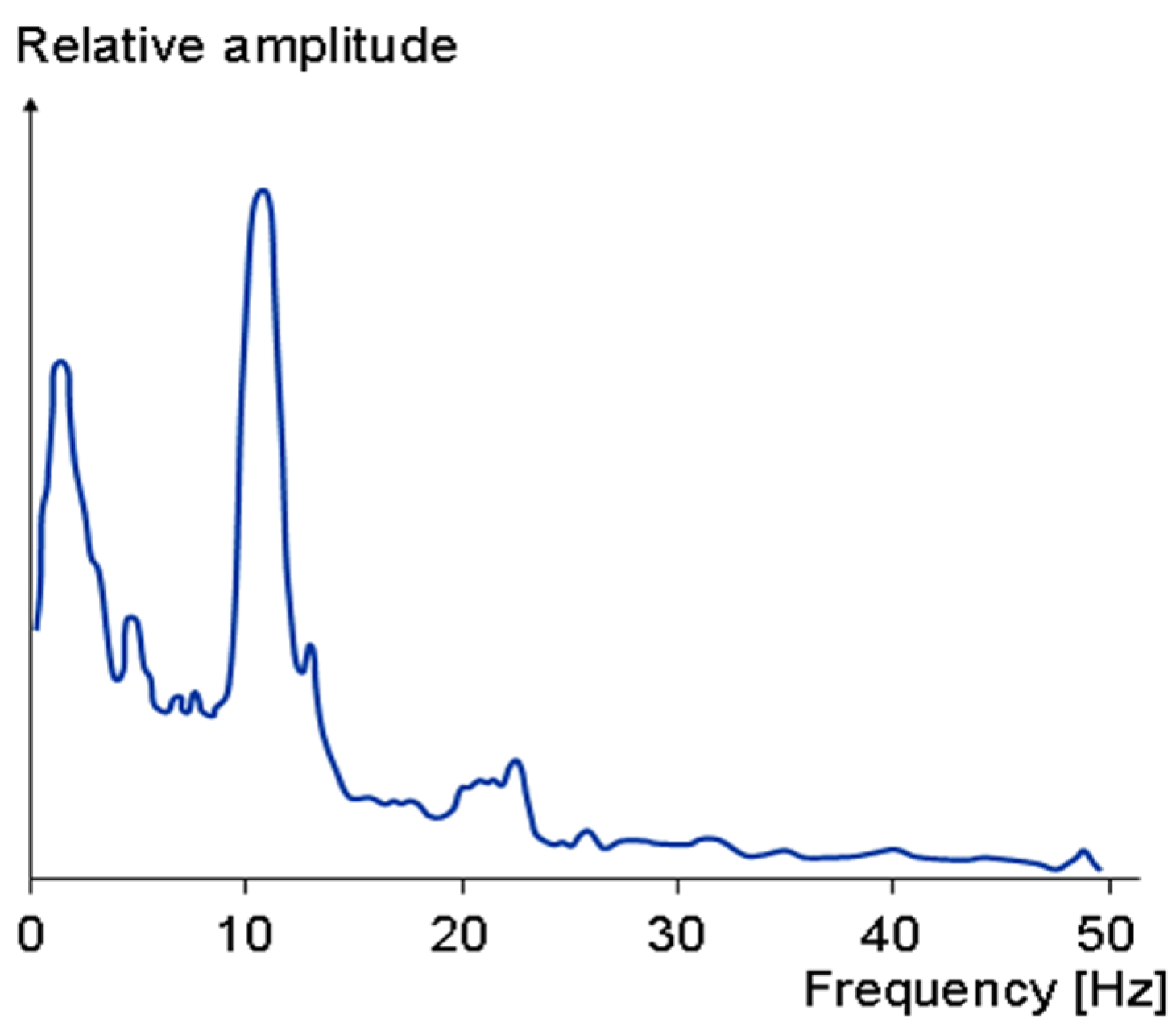
Furthermore, note that typically biomedical signals have very small amplitude and are at relatively low frequencies. For instance, the amplitude of an EEG signal is normally below 100 µV when measured on the scalp, and about 1–2 mV when measured on the surface of the brain. The frequency band of these signals is from under 1 Hz to about 50 Hz, as demonstrated in Figure 9. Similarly, the spectrum of an ECG signal is mostly distributed between 0.1 Hz to 160 Hz and its amplitude is typically below 5 mV. Thus, filtering of these signals requires filters with very small low cut-off frequency. As a result, the filter requires a very large capacitor or resistor which is hard to achieve on a limited on-chip area. To address this issue, MOS pseudo resistance with a resistance in the order of tera-ohms is used in the proposed circuit [5,29,35]. Using this technique, drastically reduces the required on-chip area to realize the capacitors and resistors of the filter.
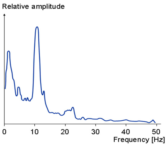
Figure 9.
The frequency spectrum of normal EEG.

Table 3.
Features of the designed CMIA compared to other works.
Table 3.
Features of the designed CMIA compared to other works.
| Parameter | Technology | Power Supply | Gain | BW (−3 dB) | On-Chip Area | Power Dissipation |
|---|---|---|---|---|---|---|
| [11] | 0.18 μm CMOS | ±0.9 V | 25–27.6 dB | 100 MHz | NA | 1.15 mW |
| [25] | 0.18 μm CMOS | ±1.2 V | 19 dB for RL = 8 KΩ | 18.1 MHz | NA | 383.4 μW |
| [33] | 0.5 μm CMOS | ±1.5 V | 9–23 dB | 20 MHz | NA, Large size, due to use 7 off-chip resistors | 3.99 mW |
| [36] | 0.18 μm CMOS | 1.8 V | Maximum of 40 dB | 2 KHz | 0.087 mm2 | 39.6 μW |
| This work | 0.18 μm CMOS | ±0.9 V | 10 dB for RL = 20 KΩ | 450 MHz | 460 μm2 | 148 μW * |
* The power consumption is reduced to about 39 µW by decreasing the supply and bias voltages. In this case, the linear dynamic range of the output voltage is restricted to ±0.3 V, and the frequency band of the flat response with a unity voltage gain is reduced to about 38 MHz.
Equations (1) and (2) are used to estimate the cut-off frequencies, and of the circuit. The resistance Rinc produced by the MOS-pseudo resistors (Ma, Mb, and MRL) is about tera-ohm. Thus, very small C1 and CZ are required to achieve the small cut-off frequencies and , respectively.
3. Results
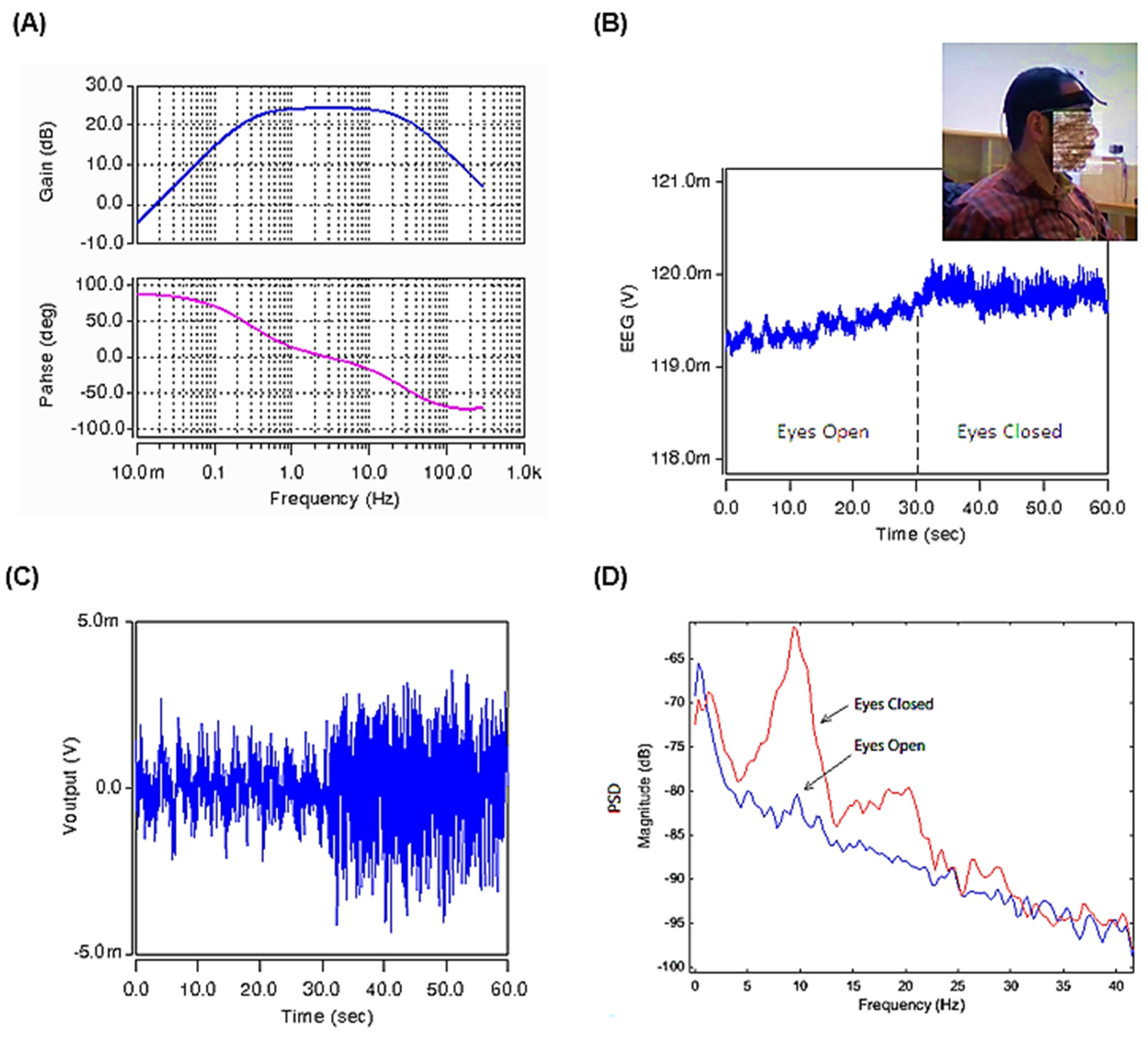
In order to validate the proposed filtering instrumental amplifier, two versions of the proposed circuit, one for filtering EEG signals and one for filtering ECG signals, are designed. Considering the typical frequency band of EEG signals (shown in Figure 9), the first circuit was designed to pass the frequency band of 0.2–30 Hz with a voltage gain of about 24.3 dB. To achieve this frequency band, the values of capacitors C1 and Cz are set to 1 pF and 1.5 pF, respectively, and W/L sizing of the MOS pseudo resistors Ma, Mb, and MRL are set to and , respectively. The frequency response of the designed band-pass IA is shown in Figure 10A. An input EEG test signal, which was recorded at the Neuro-Technology Lab in the Biomedical Engineering Department, the University of Isfahan, during the eyes-closed condition, followed by the eyes-open resting condition, was used to validate the designed circuit.

Figure 10.
(A) The frequency response of the gain and phase of the band-pass bioamplifier. (B) The original EEG input signal (Vinput) (C). The EEG output signal after amplification and filtering using the designed circuit of Figure 8. (D) Power spectral density plots under eyes-open and eyes-closed conditions for the EEG recordings.
The original EEG input signal (Vinput in Figure 8), is depicted in Figure 10B. This EEG signal was recorded at a resting-state under the eyes-open condition for about the first 30 s and then from second 30 up to second 60, it is recorded at the eyes-closed resting condition. The DC offset and baseline drift artifacts caused by the electrodes are removed at the inputs of the instrumentation amplifier at points Y1 and Y2. After removing the DC component, the signal is filtered and amplified in the desired frequency band and then appears at the Voutput.
The filtered and amplified output signal is shown in Figure 10C. It can be seen that the sample EEG input signal is a low-quality noisy signal with a DC level and drift. The results show that the proposed circuit proves its proper performance by eliminating the undesired artifact and DC component of the EEG input signal. Figure 10D shows the PSD (power spectral density) plots for the EEG signals under eyes-open and eyes-closed conditions. As we already know, the Alpha waves are reduced with open eyes, drowsiness, and sleep. The obtained results shown in the PSD plots confirm the proper work of the proposed circuit, showing the expected substantial difference in the Alpha rhythm of the EEG wave when the eyes are open compared to the eyes-closed condition.
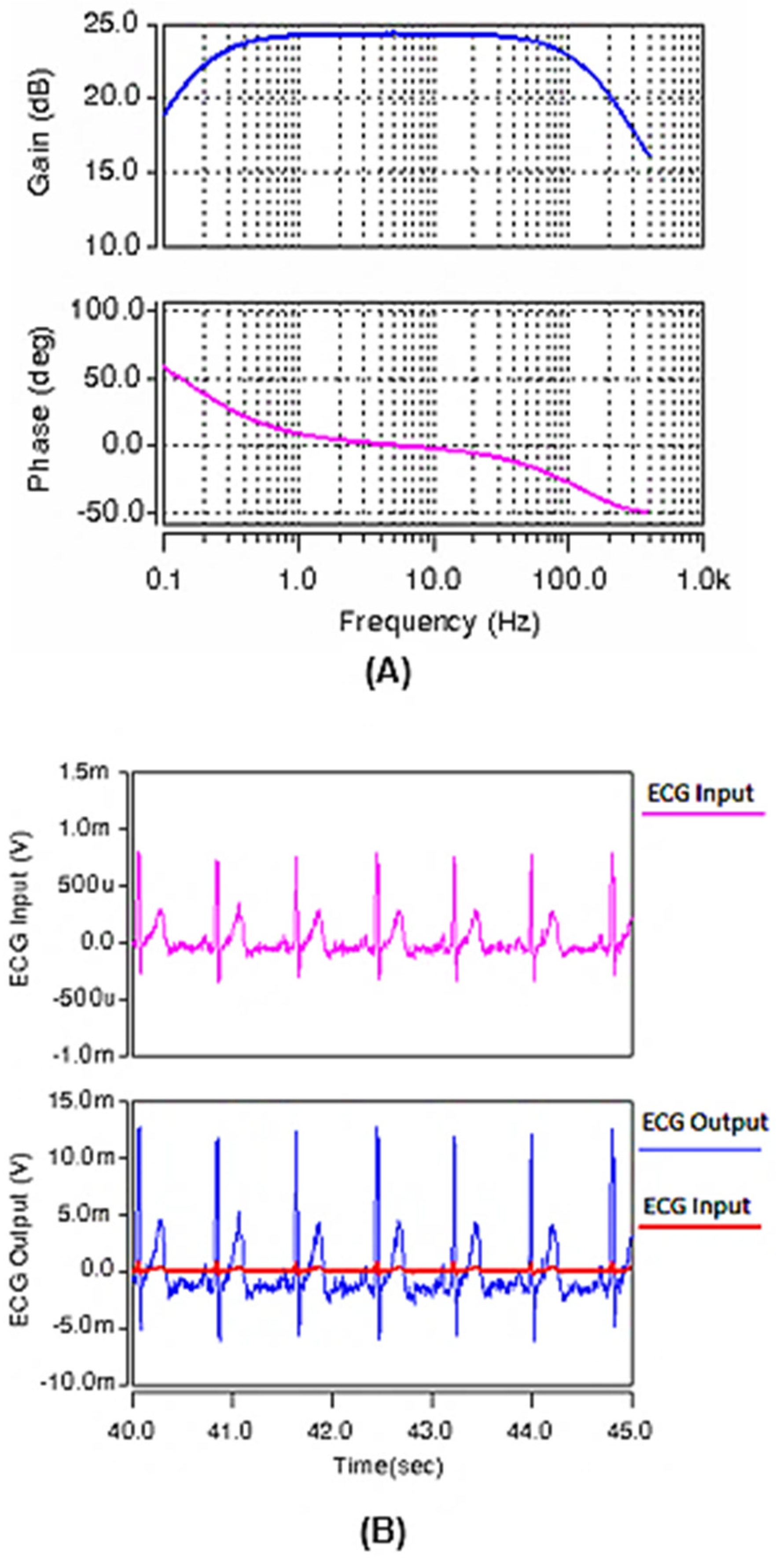
The circuit is then redesigned by changing capacitor Cz to 0.25 pF and the W/L ratio of Ma and Mb to , to pass the frequency band of 0.13–160 Hz (Figure 11A) for ECG applications. Again, an ECG sample input, recorded at the Biomedical Instrumentation Lab in the Biomedical Engineering Department, the University of Isfahan, was applied and the output signal is shown in Figure 11B. Again, the quality of the output ECG signal proves the performance of the redesigned circuit for ECG recordings.
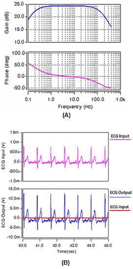
Figure 11.
(A) The frequency response of the gain and phase of the band-pass amplifier for ECG recording. (B) The ECG input and its related output signal after amplification and filtering using the designed circuit of Figure 8.
In order to investigate the distortion level of the proposed band-pass instrumentation amplifier, THD (total harmonic distortion) analysis was conducted. The analysis shows a THD of about 0.97% for a sinusoid input signal with an amplitude of 0.8 mVp-p and a frequency of 10 Hz. It is worth mentioning that this THD is small enough, and the existence of this level of distortion in a large amplitude of an ECG signal is not an issue for the diagnoses of cardiac arrhythmia and other illnesses.
4. Conclusions
In this paper, a wide range CMOS DVCC based on a wide linear range transconductor has been presented. The proposed DVCC has a wide dynamic range of ±400 mV and ±0.85 mA. Its voltage frequency response has a flat unity voltage gain (Vx/Vid) of 80 MHz. The power consumption of 148 µW was measured by a post layout simulation. The layout of the DVCC circuit occupies a total area of 0.378 µm2. In the following, using the presented DVCC, an instrumentation amplifier has been implemented and a new configuration has been presented to realize a band-pass amplifier using IA. In order to validate the proposed band-pass amplifier, two versions of the circuit with different specifications have been designed and recorded EEG and ECG signals have been successfully amplified and filtered. The proposed current-mode band-pass instrumentation amplifiers have applications in improving the quality of various biomedical signals for clinical diagnosis, including electrocardiography and electroencephalography.
Author Contributions
Conceptualization, F.K.H.; methodology, F.K.H.; software, F.K.H.; validation, F.K.H., Z.K.H. and N.B.; formal analysis, F.K.H.; investigation, Z.K.H. and N.B.; writing—original draft preparation, F.K.H.; writing—review and editing, Z.K.H. and N.B. All authors have read and agreed to the published version of the manuscript.
Funding
This research received no external funding.
Acknowledgments
The authors would like to thank Ali Karami and Mahmoud Norouzi for their precious help. The authors also thank Mohammadreza Behboodi for providing EEG and ECG samples for this research.
Conflicts of Interest
The authors declare no conflict of interest.
References
- Prats-Boluda, G.; Ye-Lin, Y.; Barrachina, J.B.; Senent, E.; de Sanabria, R.R.; Garcia-Casado, J. Development of a portable wireless system for bipolar concentric ECG recording. Meas. Sci. Technol. 2015, 26, 075102. [Google Scholar] [CrossRef]
- Ettinger, S.; Stanak, M.; Szymański, P.; Wild, C.; Haček, R.T.; Erčević, D.; Grenković, R.; Huić, M. Wearable cardioverter defibrillators for the prevention of sudden cardiac arrest: A health technology assessment and patient focus group study. Med. Devices (Auckl. NZ) 2017, 10, 257. [Google Scholar] [CrossRef] [PubMed]
- Niederhauser, T.; Haeberlin, A.; Marisa, T.; Mattle, D.; Abächerli, R.; Goette, J.; Jacomet, M.; Vogel, R. An optimized lead system for long-term esophageal electrocardiography. Physiol. Meas. 2014, 35, 517. [Google Scholar] [CrossRef]
- Kalra, A.; Lowe, A.; Al-Jumaily, A. Critical review of electrocardiography measurement systems and technology. Meas. Sci. Technol. 2018, 30, 012001. [Google Scholar] [CrossRef]
- Karami Horestani, F.; Eshghi, M.; Yazdchi, M. An ultra low power amplifier for wearable and implantable electronic devices. Microelectron. Eng. 2019, 216, 111054. [Google Scholar] [CrossRef]
- Prats-Boluda, G.; Ye-Lin, Y.; Garcia-Breijo, E.; Ibanez, J.; Garcia-Casado, J. Active flexible concentric ring electrode for non-invasive surface bioelectrical recordings. Meas. Sci. Technol. 2012, 23, 125703. [Google Scholar] [CrossRef]
- Gargiulo, G.; Bifulco, P.; Cesarelli, M.; Ruffo, M.; Romano, M.; Calvo, R.A.; Jin, C.; van Schaik, A. An ultra-high input impedance ECG amplifier for long-term monitoring of athletes. Med. Devices (Auckl. NZ) 2010, 3, 1. [Google Scholar] [CrossRef]
- Bifulco, P.; Gargiulo, G.D.; Romano, M.; Cesarelli, M. A simple, wide bandwidth, biopotential amplifier to record pacemaker pulse waveform. Med. Devices (Auckl. NZ) 2016, 9, 325. [Google Scholar]
- Rao, A.; Murphy, E.; Shahghasemi, M.; Odame, K. Current-conveyor-based wide-band current driver for electrical impedance tomography. Physiol. Meas. 2019, 40, 034005. [Google Scholar] [CrossRef]
- Mahmoud, S.A. Fully differential CMOS CCII based on differential difference transconductor. Analog Integr. Circuits Signal Process. 2007, 50, 195–203. [Google Scholar] [CrossRef]
- Chaturvedi, B.; Kumar, A. Electronically tunable current-mode instrumentation amplifier with high CMRR and wide bandwidth. AEU-Int. J. Electron. Commun. 2018, 92, 116–123. [Google Scholar] [CrossRef]
- Arora, T.S.; Gupta, S. A new voltage mode quadrature oscillator using grounded capacitors: An application of CDBA. Eng. Sci. Technol. Int. J. 2018, 21, 43–49. [Google Scholar] [CrossRef]
- Carrasco-Aguilar, M.; Sánchez-López, C.; Carbajal-Gómez, V. Pinched hysteresis behavior in a PID-controlled resistor. Eng. Sci. Technol. Int. J. 2018, 21, 297–301. [Google Scholar] [CrossRef]
- Abuelma’atti, M.T. Recent Developments in Current-Mode Sinusoidal Oscillators: Circuits and Active Elements. Arab. J. Sci. Eng. 2017, 42, 2583–2614. [Google Scholar] [CrossRef]
- Sedra, A.; Smith, K. A second-generation current conveyor and its applications. IEEE Trans. Circuit Theory 1970, 17, 132–134. [Google Scholar] [CrossRef]
- Soliman, A. New fully-differential CMOS second-generation current conveyer. Etri J. 2006, 28, 495–501. [Google Scholar]
- Madian, A.H.; Mahmoud, S.A.; Soliman, A.M. New 1.5-V CMOS second generation current conveyor based on wide range transconductor. Analog Integr. Circuits Signal Process. 2006, 49, 267–279. [Google Scholar] [CrossRef]
- Abrishamifar, A.; Karimi, Y.; Navidi, M.M. Current controlled current differential current conveyor: A novel building block for analog signal processing. IEICE Electron. Express 2012, 9, 104–110. [Google Scholar] [CrossRef][Green Version]
- Kunto, T.; Prommee, P.; Abuelma, A.; Taher, M. Electronically Tunable Current-mode High-order Ladder Low-pass Filters Based on CMOS Technology. Radioengineering 2015, 24, 974–987. [Google Scholar] [CrossRef]
- Abuelma’atti, M.T.; Bentrcia, A.; Al-Shahrani, S.A.M. A novel mixed-mode current-conveyor-based filter. Int. J. Electron. 2004, 91, 191–197. [Google Scholar] [CrossRef]
- Soliman, A.M. Current feedback operational amplifier based oscillators. Analog Integr. Circuits Signal Process. 2000, 23, 45–55. [Google Scholar] [CrossRef]
- Abuelmaatti, M.T.; Al-Qahtani, M.A. A new current-controlled multiphase sinusoidal oscillator using translinear current conveyors. IEEE Trans. Circuits Syst. II Analog Digit. Signal Process. 1998, 45, 881–885. [Google Scholar] [CrossRef]
- Safari, L.; Azhari, S. A high performance fully differential pure current mode operational amplifier and its applications. J. Eng. Sci. Technol. 2012, 7, 471–486. [Google Scholar]
- Eldeeb, M.A.; Ghallab, Y.H.; Ismail, Y.; Elghitani, H. Low-voltage subthreshold CMOS current mode circuits: Design and applications. AEU-Int. J. Electron. Commun. 2017, 82, 251–264. [Google Scholar] [CrossRef]
- Ahmadi, S.; Azhari, S.J. A novel fully differential second generation current conveyor and its application as a very high CMRR instrumentation amplifier. Emerg. Sci. J. 2018, 2, 85–92. [Google Scholar] [CrossRef]
- Elwan, H.; Soliman, A. Novel CMOS differential voltage current conveyor and its applications. IEE Proc.-Circuits Devices Syst. 1997, 144, 195–200. [Google Scholar] [CrossRef]
- Naik, A.; Devashrayee, N. Characterization of a CMOS differential current conveyor using 0.25 micron technology. Int. J. Adv. Eng. Appl. 2010, 177–182. [Google Scholar]
- Wilson, B. Universal conveyor instrumentation amplifier. Electron. Lett. 1989, 25, 470–471. [Google Scholar] [CrossRef]
- Kumar, S.; Kim, B.-S.; Song, H. An integrated approach of CNT front-end amplifier towards spikes monitoring for Neuro-prosthetic Diagnosis. BioChip J. 2018, 12, 332–339. [Google Scholar] [CrossRef]
- Hassan, T.M.; Mahmoud, S.A. New CMOS DVCC realization and applications to instrumentation amplifier and active-RC filters. AEU-Int. J. Electron. Commun. 2010, 64, 47–55. [Google Scholar] [CrossRef]
- Cini, U.; Arslan, E. A high gain and low-offset current-mode instrumentation amplifier using differential difference current conveyors. In Proceedings of the IEEE International Conference on Electronics, Circuits, and Systems (ICECS), Cairo, Egypt, 6–9 December 2015. [Google Scholar]
- Safari, L.; Yuce, E.; Minaei, S. A new transresistance-mode instrumentation amplifier with low number of MOS transistors and electronic tuning opportunity. J. Circuits Syst. Comput. 2016, 25, 1650022. [Google Scholar] [CrossRef]
- Pandey, N.; Nand, D.; Pandey, R. Generalized operational floating current conveyor based instrumentation amplifier. IET Circuits Devices Syst. 2016, 10, 209–219. [Google Scholar] [CrossRef]
- Smither, M.; Pugh, D.; Woolard, L. CMRR analysis of the 3-op-amp instrumentation amplifier. Electron. Lett. 1977, 13, 594. [Google Scholar] [CrossRef]
- Harrison, R.R.; Charles, C. A low-power low-noise CMOS amplifier for neural recording applications. IEEE J. Solid-State Circuits 2003, 38, 958–965. [Google Scholar] [CrossRef]
- Ong, G.T.; Chan, P.K. A power-aware chopper-stabilized instrumentationamplifier for resistive wheatstone bridge sensors. IEEE Trans. Instrum. Meas. 2014, 63, 2253–2263. [Google Scholar] [CrossRef]
Publisher’s Note: MDPI stays neutral with regard to jurisdictional claims in published maps and institutional affiliations. |
© 2022 by the authors. Licensee MDPI, Basel, Switzerland. This article is an open access article distributed under the terms and conditions of the Creative Commons Attribution (CC BY) license (https://creativecommons.org/licenses/by/4.0/).

