
A Band-Pass Instrumentation Amplifier Based on a Differential Voltage Current Conveyor for Biomedical Signal Recording Applications


Abstract
1. Introduction
2. Methods
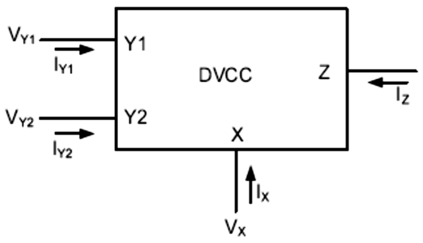
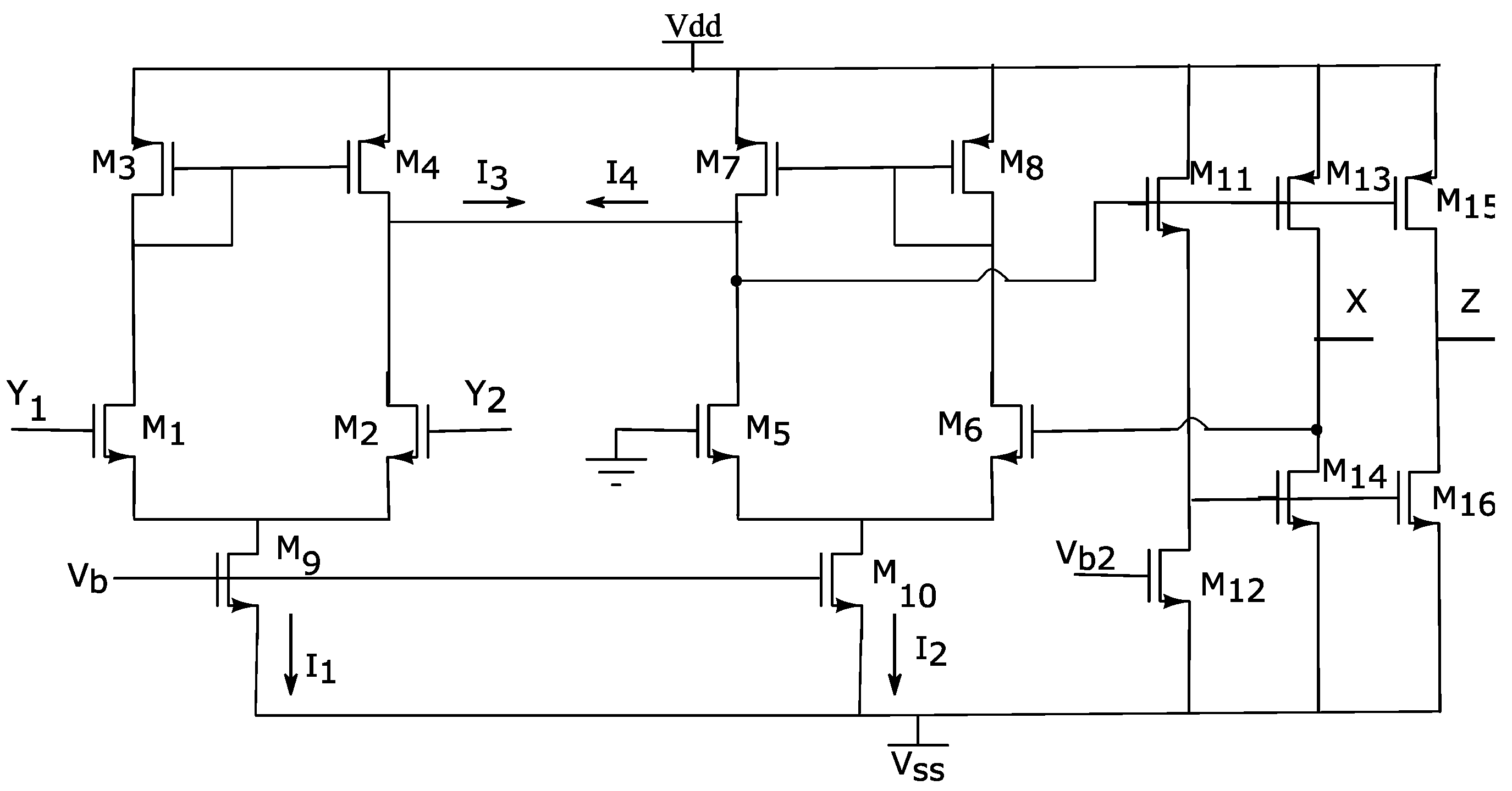
2.1. DVCCII Circuit
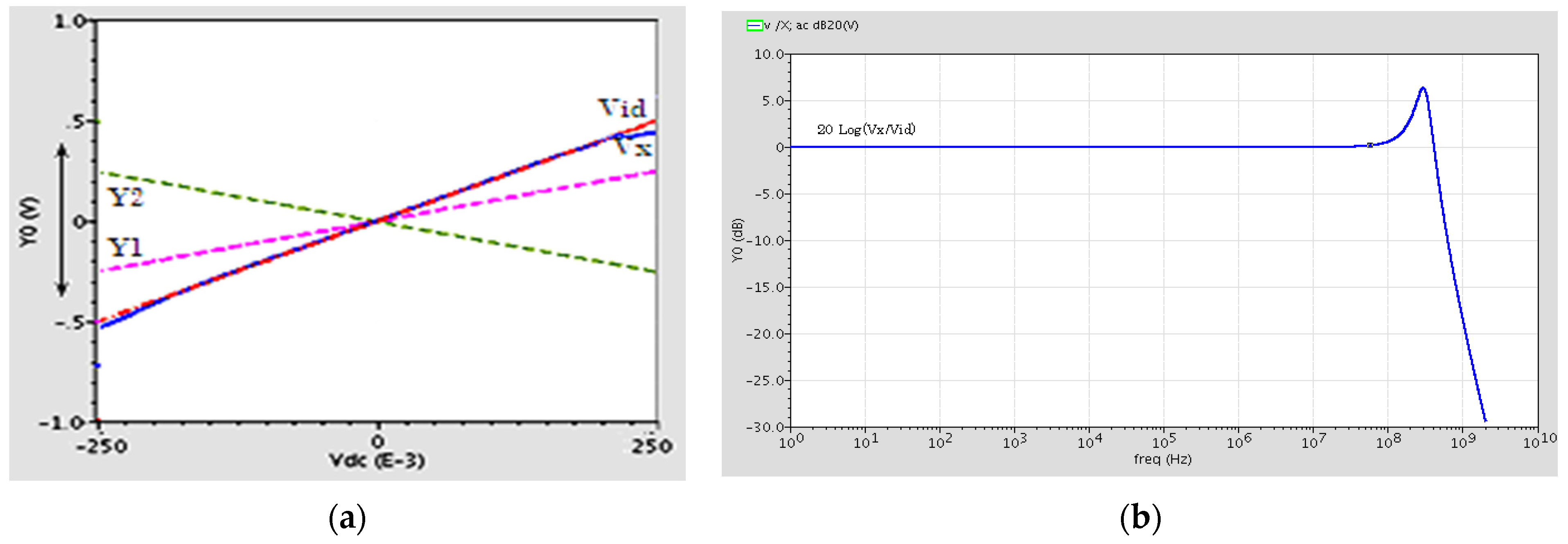
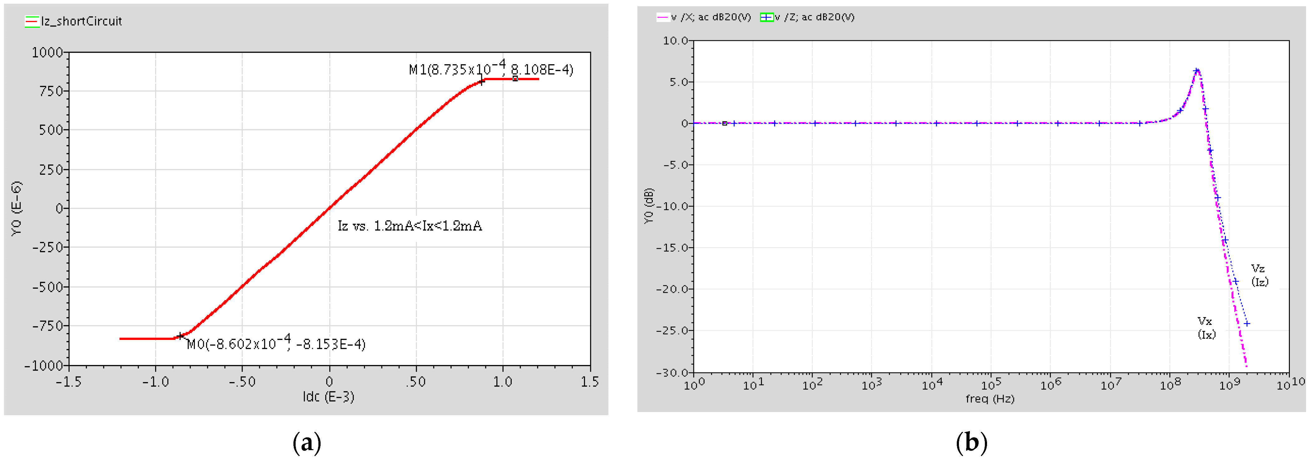
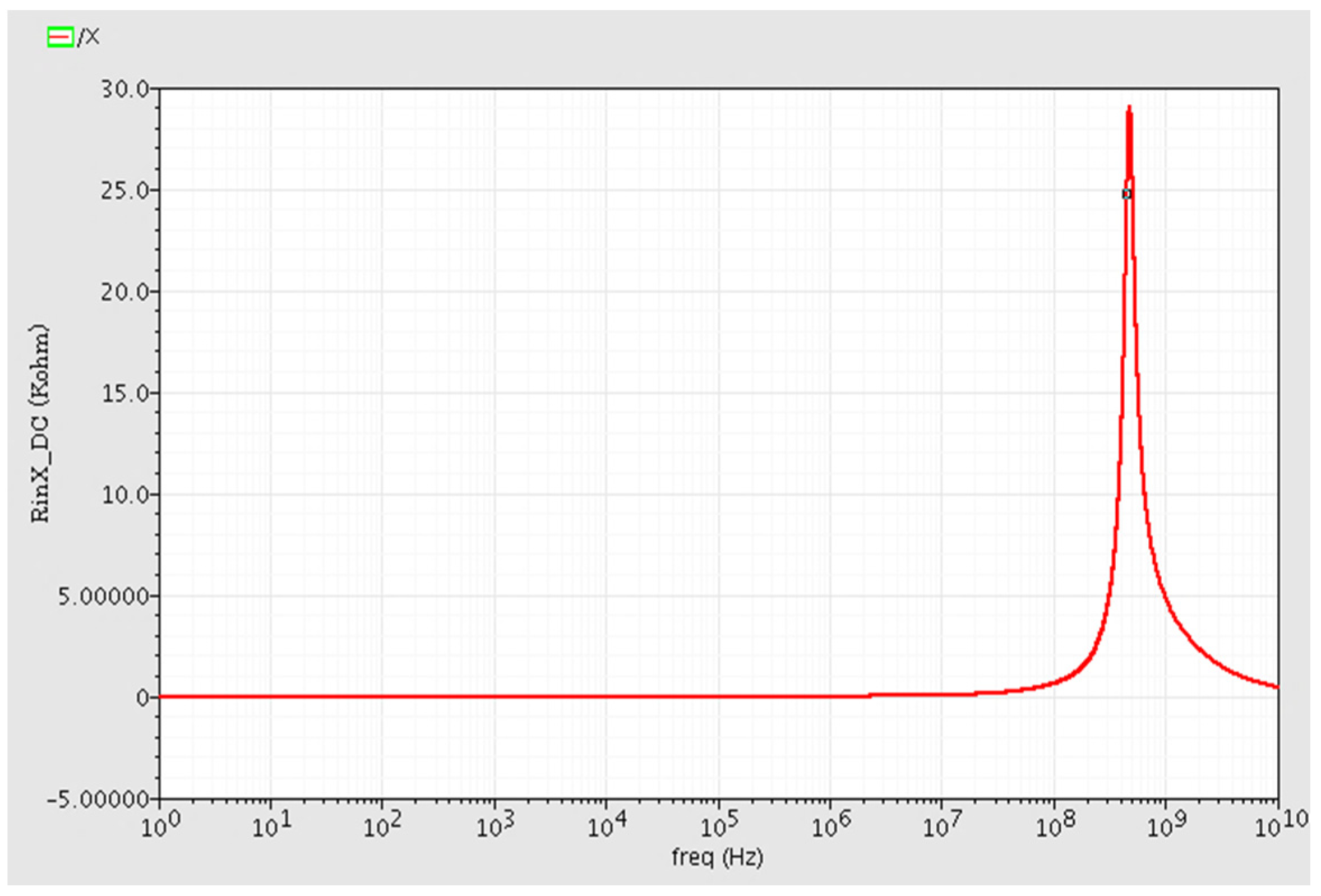
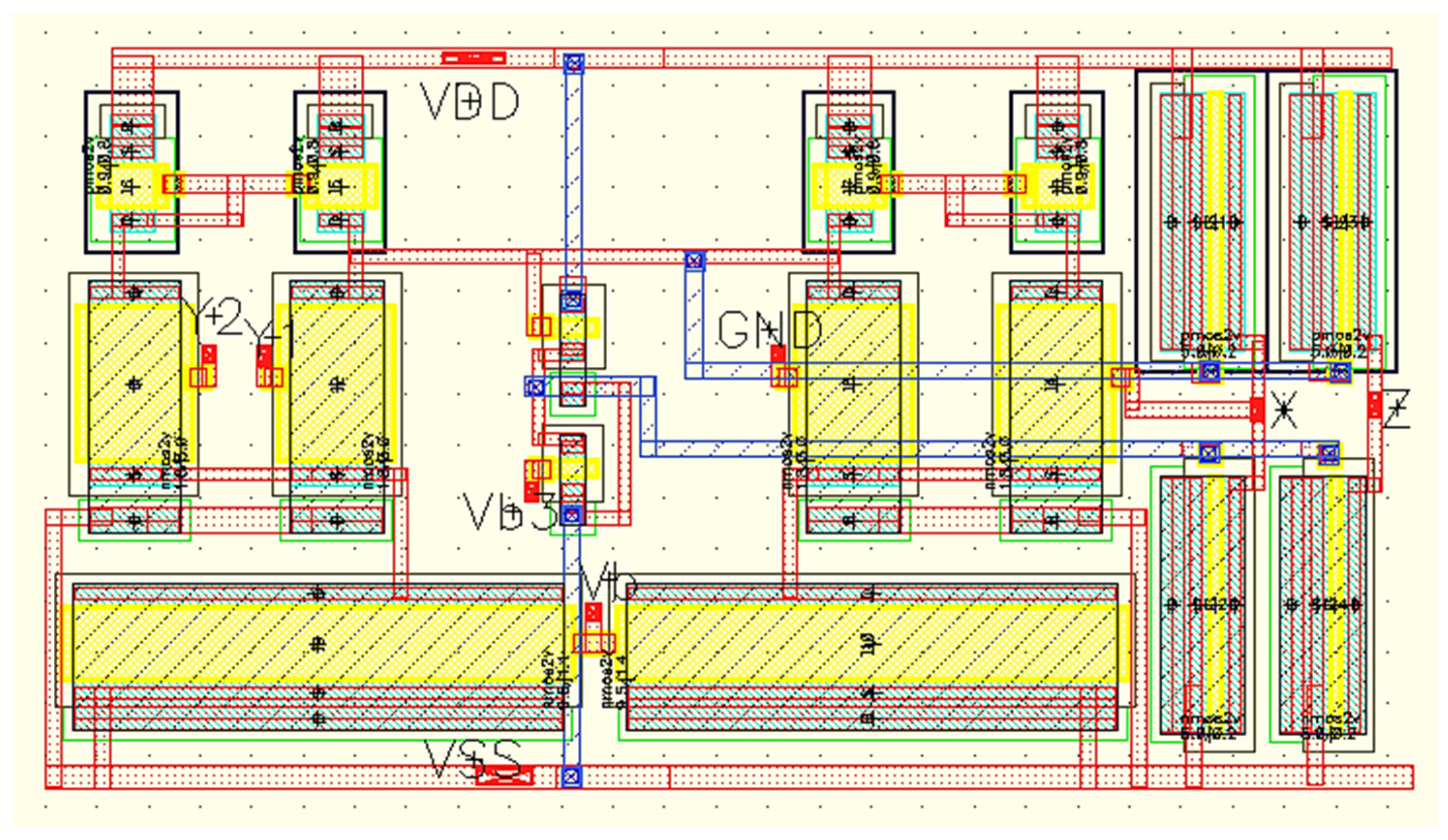
2.2. Post Layout Simulation Results
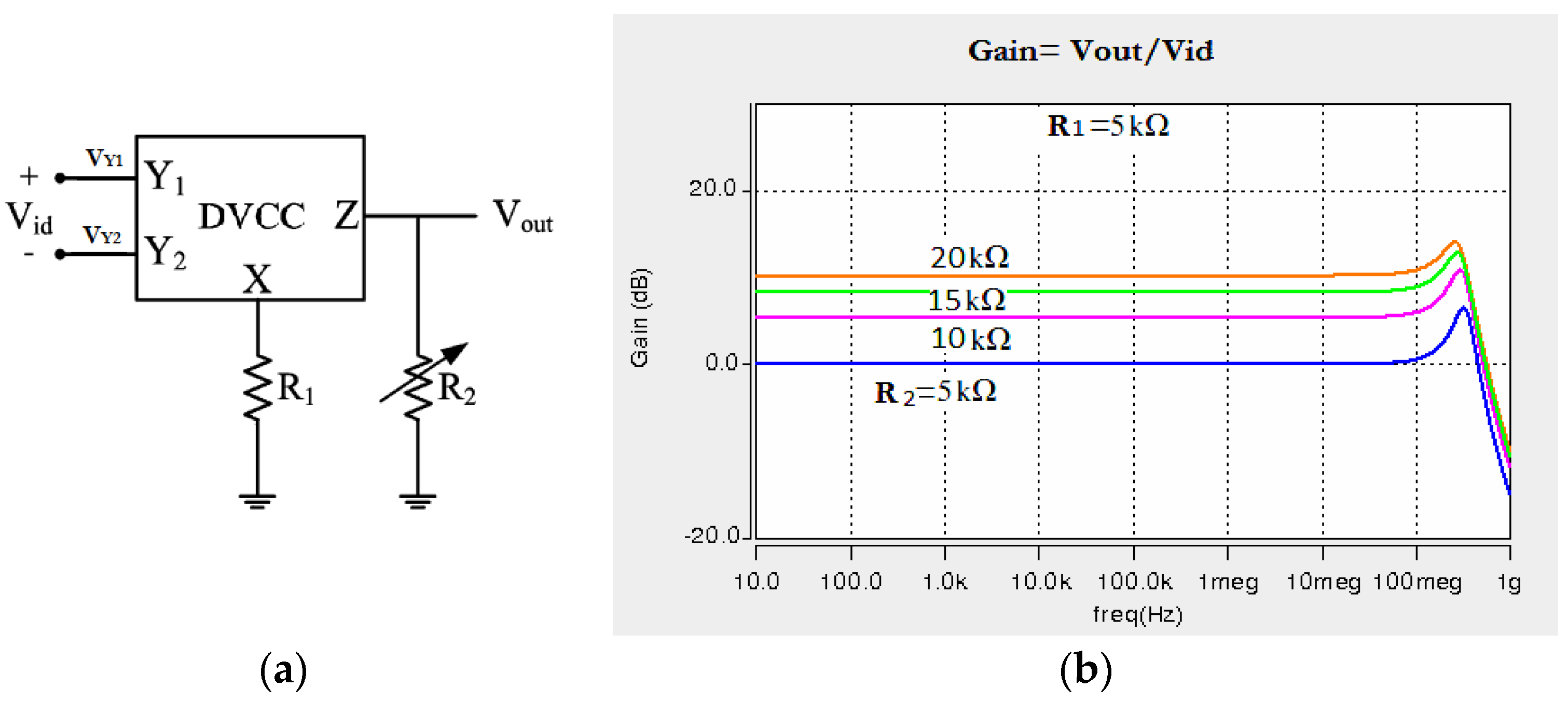
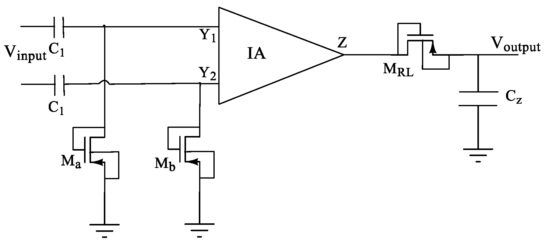
2.3. Design of DVCC-Based Instrumentation Amplifier

| Parameter | Technology | Power Supply | Gain | BW (−3 dB) | On-Chip Area | Power Dissipation |
|---|---|---|---|---|---|---|
| [11] | 0.18 μm CMOS | ±0.9 V | 25–27.6 dB | 100 MHz | NA | 1.15 mW |
| [25] | 0.18 μm CMOS | ±1.2 V | 19 dB for RL = 8 KΩ | 18.1 MHz | NA | 383.4 μW |
| [33] | 0.5 μm CMOS | ±1.5 V | 9–23 dB | 20 MHz | NA, Large size, due to use 7 off-chip resistors | 3.99 mW |
| [36] | 0.18 μm CMOS | 1.8 V | Maximum of 40 dB | 2 KHz | 0.087 mm2 | 39.6 μW |
| This work | 0.18 μm CMOS | ±0.9 V | 10 dB for RL = 20 KΩ | 450 MHz | 460 μm2 | 148 μW * |
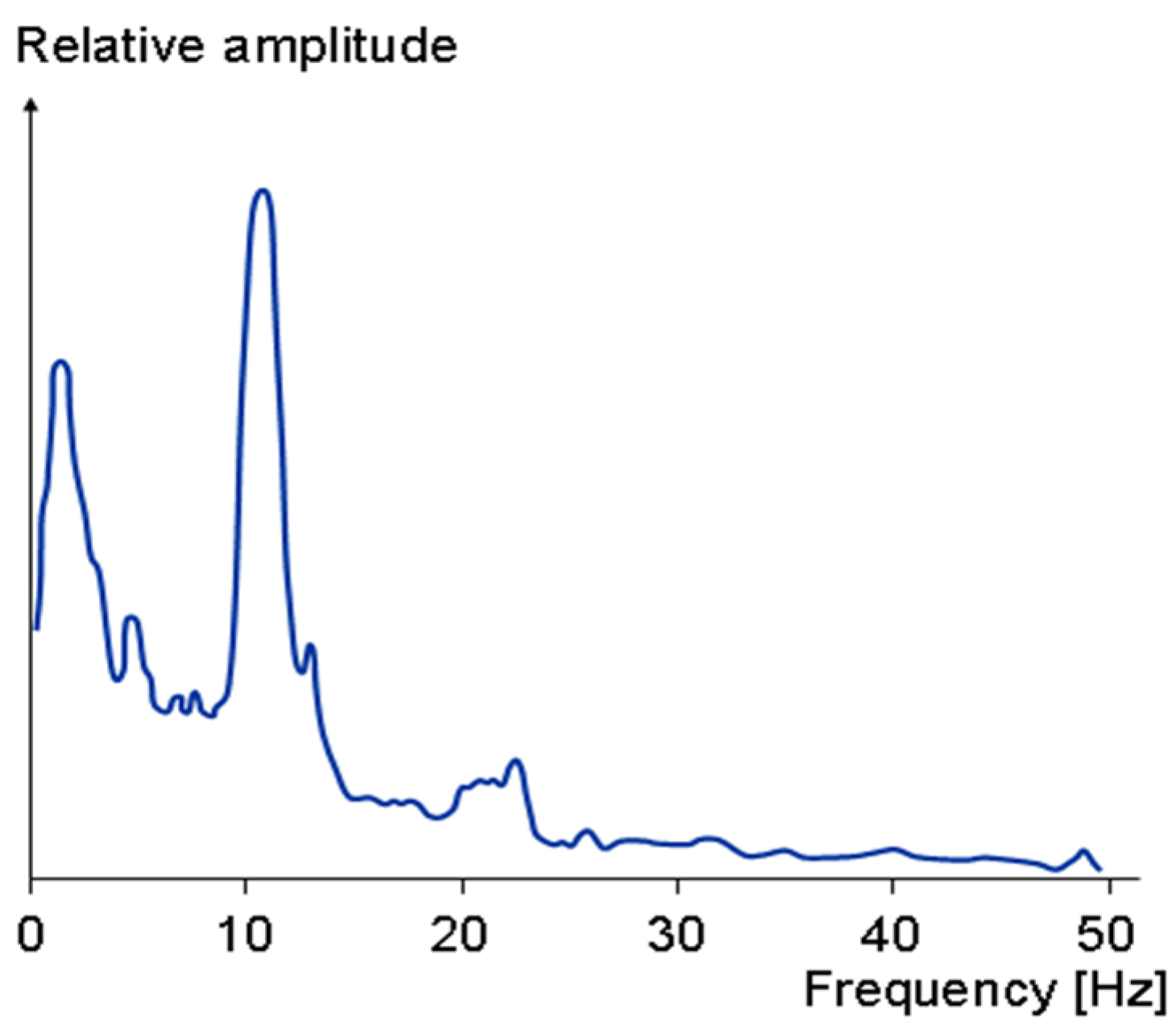
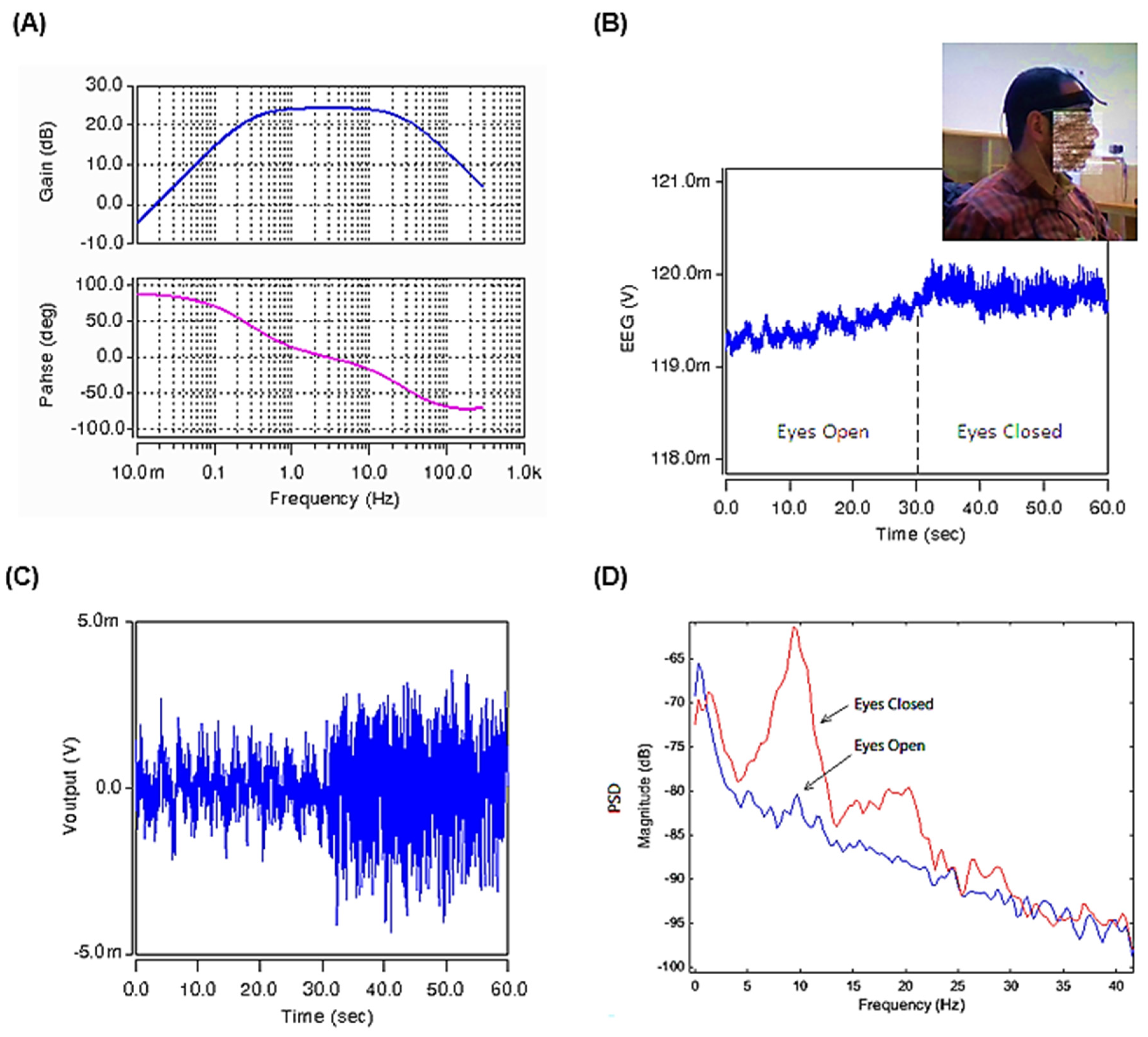
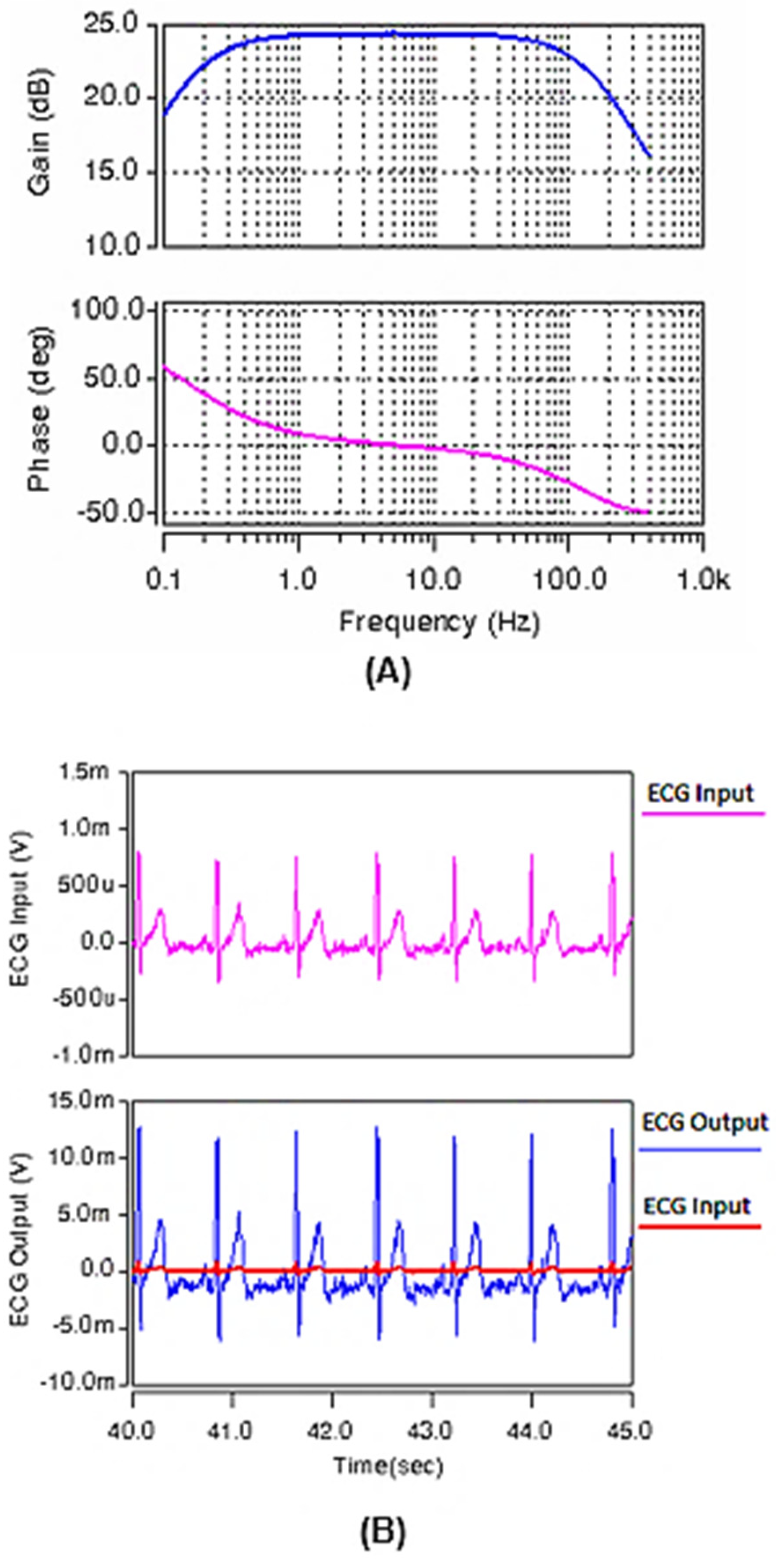
3. Results
4. Conclusions
Author Contributions
Funding
Acknowledgments
Conflicts of Interest
References
- Prats-Boluda, G.; Ye-Lin, Y.; Barrachina, J.B.; Senent, E.; de Sanabria, R.R.; Garcia-Casado, J. Development of a portable wireless system for bipolar concentric ECG recording. Meas. Sci. Technol. 2015, 26, 075102. [Google Scholar] [CrossRef]
- Ettinger, S.; Stanak, M.; Szymański, P.; Wild, C.; Haček, R.T.; Erčević, D.; Grenković, R.; Huić, M. Wearable cardioverter defibrillators for the prevention of sudden cardiac arrest: A health technology assessment and patient focus group study. Med. Devices (Auckl. NZ) 2017, 10, 257. [Google Scholar] [CrossRef] [PubMed]
- Niederhauser, T.; Haeberlin, A.; Marisa, T.; Mattle, D.; Abächerli, R.; Goette, J.; Jacomet, M.; Vogel, R. An optimized lead system for long-term esophageal electrocardiography. Physiol. Meas. 2014, 35, 517. [Google Scholar] [CrossRef]
- Kalra, A.; Lowe, A.; Al-Jumaily, A. Critical review of electrocardiography measurement systems and technology. Meas. Sci. Technol. 2018, 30, 012001. [Google Scholar] [CrossRef]
- Karami Horestani, F.; Eshghi, M.; Yazdchi, M. An ultra low power amplifier for wearable and implantable electronic devices. Microelectron. Eng. 2019, 216, 111054. [Google Scholar] [CrossRef]
- Prats-Boluda, G.; Ye-Lin, Y.; Garcia-Breijo, E.; Ibanez, J.; Garcia-Casado, J. Active flexible concentric ring electrode for non-invasive surface bioelectrical recordings. Meas. Sci. Technol. 2012, 23, 125703. [Google Scholar] [CrossRef]
- Gargiulo, G.; Bifulco, P.; Cesarelli, M.; Ruffo, M.; Romano, M.; Calvo, R.A.; Jin, C.; van Schaik, A. An ultra-high input impedance ECG amplifier for long-term monitoring of athletes. Med. Devices (Auckl. NZ) 2010, 3, 1. [Google Scholar] [CrossRef]
- Bifulco, P.; Gargiulo, G.D.; Romano, M.; Cesarelli, M. A simple, wide bandwidth, biopotential amplifier to record pacemaker pulse waveform. Med. Devices (Auckl. NZ) 2016, 9, 325. [Google Scholar]
- Rao, A.; Murphy, E.; Shahghasemi, M.; Odame, K. Current-conveyor-based wide-band current driver for electrical impedance tomography. Physiol. Meas. 2019, 40, 034005. [Google Scholar] [CrossRef]
- Mahmoud, S.A. Fully differential CMOS CCII based on differential difference transconductor. Analog Integr. Circuits Signal Process. 2007, 50, 195–203. [Google Scholar] [CrossRef]
- Chaturvedi, B.; Kumar, A. Electronically tunable current-mode instrumentation amplifier with high CMRR and wide bandwidth. AEU-Int. J. Electron. Commun. 2018, 92, 116–123. [Google Scholar] [CrossRef]
- Arora, T.S.; Gupta, S. A new voltage mode quadrature oscillator using grounded capacitors: An application of CDBA. Eng. Sci. Technol. Int. J. 2018, 21, 43–49. [Google Scholar] [CrossRef]
- Carrasco-Aguilar, M.; Sánchez-López, C.; Carbajal-Gómez, V. Pinched hysteresis behavior in a PID-controlled resistor. Eng. Sci. Technol. Int. J. 2018, 21, 297–301. [Google Scholar] [CrossRef]
- Abuelma’atti, M.T. Recent Developments in Current-Mode Sinusoidal Oscillators: Circuits and Active Elements. Arab. J. Sci. Eng. 2017, 42, 2583–2614. [Google Scholar] [CrossRef]
- Sedra, A.; Smith, K. A second-generation current conveyor and its applications. IEEE Trans. Circuit Theory 1970, 17, 132–134. [Google Scholar] [CrossRef]
- Soliman, A. New fully-differential CMOS second-generation current conveyer. Etri J. 2006, 28, 495–501. [Google Scholar]
- Madian, A.H.; Mahmoud, S.A.; Soliman, A.M. New 1.5-V CMOS second generation current conveyor based on wide range transconductor. Analog Integr. Circuits Signal Process. 2006, 49, 267–279. [Google Scholar] [CrossRef]
- Abrishamifar, A.; Karimi, Y.; Navidi, M.M. Current controlled current differential current conveyor: A novel building block for analog signal processing. IEICE Electron. Express 2012, 9, 104–110. [Google Scholar] [CrossRef][Green Version]
- Kunto, T.; Prommee, P.; Abuelma, A.; Taher, M. Electronically Tunable Current-mode High-order Ladder Low-pass Filters Based on CMOS Technology. Radioengineering 2015, 24, 974–987. [Google Scholar] [CrossRef]
- Abuelma’atti, M.T.; Bentrcia, A.; Al-Shahrani, S.A.M. A novel mixed-mode current-conveyor-based filter. Int. J. Electron. 2004, 91, 191–197. [Google Scholar] [CrossRef]
- Soliman, A.M. Current feedback operational amplifier based oscillators. Analog Integr. Circuits Signal Process. 2000, 23, 45–55. [Google Scholar] [CrossRef]
- Abuelmaatti, M.T.; Al-Qahtani, M.A. A new current-controlled multiphase sinusoidal oscillator using translinear current conveyors. IEEE Trans. Circuits Syst. II Analog Digit. Signal Process. 1998, 45, 881–885. [Google Scholar] [CrossRef]
- Safari, L.; Azhari, S. A high performance fully differential pure current mode operational amplifier and its applications. J. Eng. Sci. Technol. 2012, 7, 471–486. [Google Scholar]
- Eldeeb, M.A.; Ghallab, Y.H.; Ismail, Y.; Elghitani, H. Low-voltage subthreshold CMOS current mode circuits: Design and applications. AEU-Int. J. Electron. Commun. 2017, 82, 251–264. [Google Scholar] [CrossRef]
- Ahmadi, S.; Azhari, S.J. A novel fully differential second generation current conveyor and its application as a very high CMRR instrumentation amplifier. Emerg. Sci. J. 2018, 2, 85–92. [Google Scholar] [CrossRef]
- Elwan, H.; Soliman, A. Novel CMOS differential voltage current conveyor and its applications. IEE Proc.-Circuits Devices Syst. 1997, 144, 195–200. [Google Scholar] [CrossRef]
- Naik, A.; Devashrayee, N. Characterization of a CMOS differential current conveyor using 0.25 micron technology. Int. J. Adv. Eng. Appl. 2010, 177–182. [Google Scholar]
- Wilson, B. Universal conveyor instrumentation amplifier. Electron. Lett. 1989, 25, 470–471. [Google Scholar] [CrossRef]
- Kumar, S.; Kim, B.-S.; Song, H. An integrated approach of CNT front-end amplifier towards spikes monitoring for Neuro-prosthetic Diagnosis. BioChip J. 2018, 12, 332–339. [Google Scholar] [CrossRef]
- Hassan, T.M.; Mahmoud, S.A. New CMOS DVCC realization and applications to instrumentation amplifier and active-RC filters. AEU-Int. J. Electron. Commun. 2010, 64, 47–55. [Google Scholar] [CrossRef]
- Cini, U.; Arslan, E. A high gain and low-offset current-mode instrumentation amplifier using differential difference current conveyors. In Proceedings of the IEEE International Conference on Electronics, Circuits, and Systems (ICECS), Cairo, Egypt, 6–9 December 2015. [Google Scholar]
- Safari, L.; Yuce, E.; Minaei, S. A new transresistance-mode instrumentation amplifier with low number of MOS transistors and electronic tuning opportunity. J. Circuits Syst. Comput. 2016, 25, 1650022. [Google Scholar] [CrossRef]
- Pandey, N.; Nand, D.; Pandey, R. Generalized operational floating current conveyor based instrumentation amplifier. IET Circuits Devices Syst. 2016, 10, 209–219. [Google Scholar] [CrossRef]
- Smither, M.; Pugh, D.; Woolard, L. CMRR analysis of the 3-op-amp instrumentation amplifier. Electron. Lett. 1977, 13, 594. [Google Scholar] [CrossRef]
- Harrison, R.R.; Charles, C. A low-power low-noise CMOS amplifier for neural recording applications. IEEE J. Solid-State Circuits 2003, 38, 958–965. [Google Scholar] [CrossRef]
- Ong, G.T.; Chan, P.K. A power-aware chopper-stabilized instrumentationamplifier for resistive wheatstone bridge sensors. IEEE Trans. Instrum. Meas. 2014, 63, 2253–2263. [Google Scholar] [CrossRef]


| Transistors | W (µm) | L (µm) |
|---|---|---|
| M1–M4 | 1.8 | 3 |
| M5–M8 | 0.9 | 0.8 |
| M9–M10 | 9.5 | 1.4 |
| M11–M12 | 0.5 | 0.3 |
| M13–M16 | 5 | 0.2 |
| Parameter | Value |
|---|---|
| Technology | 0.18 μm TSMC CMOS |
| Power Supply | ±0.9 V |
| Linear Dynamic Range for Vx vs. Vid | ±400 mV |
| X Terminal Offset Voltage | 2.24 mV |
| Linear Dynamic Range for Iz vs. Iz | −0.85 mA~0.87 mA |
| X Terminal Voltage BW, fu | BW = 450 MHz, fu = 80 MHz |
| Z Terminal Current BW, fu | BW = 450 MHz, fu = 80 MHz |
| RinX (X Terminal Input Resistance) | f < 1 MHz: R = 20 ohm f up to 100 MHz: R < 600 ohm |
| On-chip area | 378 μm2 |
| Total Power Dissipation | 148 μW |
Publisher’s Note: MDPI stays neutral with regard to jurisdictional claims in published maps and institutional affiliations. |
© 2022 by the authors. Licensee MDPI, Basel, Switzerland. This article is an open access article distributed under the terms and conditions of the Creative Commons Attribution (CC BY) license (https://creativecommons.org/licenses/by/4.0/).
Share and Cite
Karami Horestani, F.; Karami Horastani, Z.; Björsell, N. A Band-Pass Instrumentation Amplifier Based on a Differential Voltage Current Conveyor for Biomedical Signal Recording Applications. Electronics 2022, 11, 1087. https://doi.org/10.3390/electronics11071087
Karami Horestani F, Karami Horastani Z, Björsell N. A Band-Pass Instrumentation Amplifier Based on a Differential Voltage Current Conveyor for Biomedical Signal Recording Applications. Electronics. 2022; 11(7):1087. https://doi.org/10.3390/electronics11071087
Chicago/Turabian StyleKarami Horestani, Fatemeh, Zahra Karami Horastani, and Niclas Björsell. 2022. "A Band-Pass Instrumentation Amplifier Based on a Differential Voltage Current Conveyor for Biomedical Signal Recording Applications" Electronics 11, no. 7: 1087. https://doi.org/10.3390/electronics11071087
APA StyleKarami Horestani, F., Karami Horastani, Z., & Björsell, N. (2022). A Band-Pass Instrumentation Amplifier Based on a Differential Voltage Current Conveyor for Biomedical Signal Recording Applications. Electronics, 11(7), 1087. https://doi.org/10.3390/electronics11071087