Article

Design of Compact Complex Impedance Transformer with Frequency and Terminal Impedance Tunability

School of Information Science and Technology, Dalian Maritime University, Dalian 116026, China
*
Author to whom correspondence should be addressed.
Electronics 2022, 11(7), 983; https://doi.org/10.3390/electronics11070983
Submission received: 14 February 2022 / Revised: 12 March 2022 / Accepted: 21 March 2022 / Published: 22 March 2022
(This article belongs to the Section Microwave and Wireless Communications)

Abstract

:
In the paper, a compact complex impedance transformer (CIT) composed of the cascading of three varactors loaded coupled lines and two variable shunt susceptances was proposed. Highly flexible tunability functions including only frequency tunable, only impedance tunable, and both frequency and impedance tunable can be achieved by tuning the capacitance of two types of varactors and the value of the susceptance. Design equations were derived using the even–odd mode analysis and examples are given for descripting the design procedures. For validation, a prototype was designed and fabricated. During measurement, three cases were exhibited. When the termination impedance was fixed, the measured center frequency can be tuned in the range of 1.1–2.1 GHz (62.5%). When the frequency was determined, different terminal impedances can be matched by the prototype. The function of frequency tunable at different terminal impedances is also trated by the measured results. After comparison, the potential of the proposed CIT for applications in radio frequency front-end were demonstrated.

Graphical Abstract

1. Introduction

Impedance transformer [1,2] is an indispensable module in radio frequency front-end, wireless power transfer [3,4] and monolithic microwave integrated circuits. In recent years, because the impedances of the devices (such as mixers, power amplifiers, and crystal diodes) are always in a complex number, the research on complex impedance transformers (CITs) has received a lot of attention.
Generally, transmission lines (TLs) [5,6,7,8] are used for constructing CITs. In Ahn and Tentzeris [5], CIT with only one TL section was proposed. To solve the transforming range restrictions of the one TL section CIT, another TL and open/short stubs were added on the TL. Dual frequency CITs can also be obtained by TLs. In Manoochehri et al. [6], a Π-model dual-band CIT was presented to match two unequal arbitrary complex loads at two frequencies. Later, a dual-band CIT with selectable transmission zero was presented, which was composed of three sections of TLs and two shunt stubs [7]. In Xie et al. [8], parallel TLs were introduced for dual-frequency design. Except of TLs, coupled lines (CLs) can also be the candidate. For example, the miniaturized CIT based on modified CL [9] and the arbitrary terminated CIT based on susceptance loaded CL [10]. Although single- and dual-frequency CITs can be realized by TLs and CLs, they only work for one group of complex impedances with predefined frequency when the dimension is fixed. No tunability is found for the frequency and the terminal impedance.
Due to the recent trend of multifunctional and multistandard RF front-ends in communication systems, there is an increasing demand for controllable or reconfigurable devices. Tunable CITs or impedance matching networks (IMNs) are popular for unlimited power transmission, antenna matching [11], tunable power amplifiers [12,13], duplexers [14], and on-chip noise measurement systems [15,16].
At present, the research on tunable CITs are mainly focused on frequency tunable and impedance tunable. In EI-Nozahi et al. [17], a reconfigurable IMN was proposed by using the tunable inductor implemented by common drain configuration. However, the inductive behavior was affected by the parasitic capacitance at higher frequencies. In Zhang et al. [18], by using one pin diode, the adjustment characteristics at two frequency points were achieved. In Lee and Lin [19], a novel pin inductor was proposed and applied for tunable wideband IMN with a tuning range of 2.8 GHz to 4.4 GHz. Whereas, the transformation is limited to real impedances. By mploying pin diodes as switching components, a digitally-controlled impedance tunable IMN was introduced [20]. Although over 60% Smith chart coverage was achieved, the optimization process is complex. In Fouladi et al. [21], an 8-bit impedance switched IMN based on the distributed microelectromechanical transmission line was proposed with a maximum standing wave ratio of 11.5:1. In Hoarau et al. [22], a tunable IMN was proposed, which transformed the impedances varying from 6 Ω to 1 kΩ and tuned in a 50% bandwidth. Unfortunately, the bandwidth was narrow (<2%). In Lu et al. [23], an impedance tunable IMN based on the combination of transmission line, capacitors, MEMS-based switches, and inductors was proposed. In Tombak [24], an impedance tunable IMN based on ferroelectric capacitors was designed. In Arabi et al. [25], the coverage of the Smith chart of four commonly used IMNs, such as typical T, Pi, ladder, and hybrid Pi, was studied in depth. In Shen and Barker [26], a tunable IMN implemented with minimal-contact RF-MEMS switches was proposed, which demonstrated excellent coverage of the Smith chart out to a maximum VSWR of 12:1 and covered a broad frequency range extending from 10 to 50 GHz. In Jeong et al. [27], impedance tunable IMN using a transmission line with variable characteristic impedance was presented, where the variable characteristic impedance was achieved by using parallel combinations of multiple transmission lines controlled by the RF switch. In Suvarna et al. [28], an integrated transformer-based tunable IMN was described. The real and imaginary parts of the impedance can be tuned independently. However, the reported works in [23,24,25,26,27,28] only exhibited the function of impedance tuning; the feature of frequency tunable was unrealizable.
In the paper, a novel frequency and terminal impedance tunable CIT is proposed with compact structure and enhanced bandwidth. It is composed of the cascading of three varactors loaded lines, and two variable shunt susceptances. By tuning the capacitance of two types of varactors and the value of the susceptance, highly flexible tunability can be obtained, including only frequency tunable, only impedance tunable, and both frequency and impedance tunable. The content of the paper is as follows: Section 2 derives the mathematical analysis of the proposed tunable CIT through even and odd mode analysis. Section 3 gives the parameter analysis and design procedure. A prototype is designed and implemented in Section 4 for validation, followed by a conclusion in Section 5.

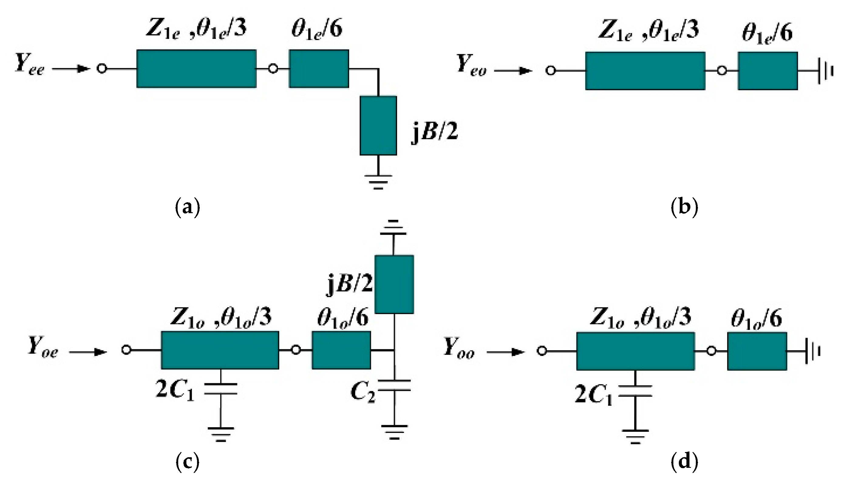
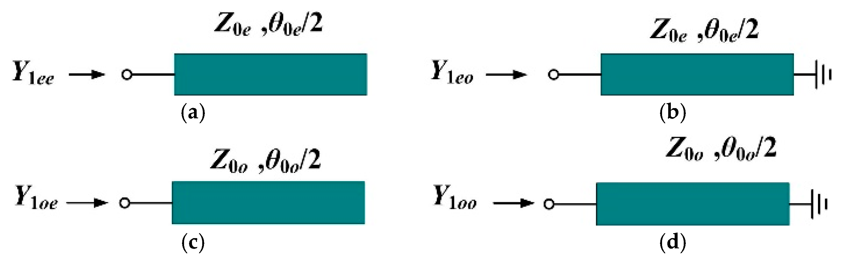
2. Design Methodology

Figure 1 shows the schematic diagram of the tunable CIT, which is composed of the cascading of three varactors loaded coupled lines and two variable shunt susceptances. It can realize the transformation from real impedance to complex impedance. The even- and odd- mode characteristic impedances of the coupled lines with electrical length of θ1 are Z1e, and Z1o, respectively. The varactors C1 are shunt between the center of the first and third coupled line sections, whereas the varactor C2 is shunt between the center of the second coupled line. The susceptance defined as B is connected in parallel in the middle of the second coupled line. Let Zg be the impedance at port 1, and ZL (ZL = RL + jXL) be the impedance at port 2.
To simplify the analysis, equivalization was applied. When considering the proposed CIT as a four-port network, it can be equivalent to a parallel coupled line with the electrical length of θ0, the even-mode characteristic impedance of Z0e, and the odd-mode characteristic impedance of Z0o, as shown in Figure 1. Then, using the even–odd mode analysis, the relations of the circuit parameters for the two four-port networks can be firstly expressed, as shown in Equations (1)–(4). Here, the condition of θ1e = θ1o = θ1 is applied for simplification. Detailed derivations can be found in Appendix A.
Y 1 e = Y 0 e cot θ 0 e 2 cot θ 1 2
B = 2 Y 1 e tan 2 θ 0 e 2 tan 2 θ 1 2 tan θ 1 2 tan 2 θ 0 e 2 + 1
C 1 = Y 1 o 2 tan θ 1 6 cot θ 1 3 + Y 1 o Y 0 o cot θ 0 o 2 1 + cot θ 1 3 tan θ 1 6 4 π f 0 Y 0 o tan θ 1 6 cot θ 0 o 2 Y 1 o
C 2 = m Y 1 o Y 1 o tan θ 1 3 B 2 m tan θ 1 3 + 1 2 π f 0 1 + m tan θ 1 3
where:
m = Y 1 o Y 0 o tan θ 0 o 2 4 π f 0 C 1 Y 0 o tan θ 1 6 tan θ 0 o 2 4 π f 0 C 1 Y 1 o Y 1 o 2 tan θ 1 6 Y 1 o 2 + Y 1 o Y 0 o tan θ 0 o 2 tan θ 1 6
It is observed from Equations (1)–(4) that by using the equivalization method, the analysis of the proposed tunable CIT can be changed to the analysis of a parallel coupled line. Thus, the input port impedance is expressed according to Jensen et al. [29].
Z in = V 1 I 1 = Z 11 Z L + Z 11 Z 22 Z 12 Z 21 Z L + Z 22
where:
Z 11 = Z 22 = 1 2 j Z 0 e cot θ 0 e + Z 0 o cot θ 0 o
Z 12 = Z 21 = 1 2 j ( Z 0 e cot θ 0 e Z 0 o cot θ 0 o )
θ 0 e = θ 0 = θ 0 o 2 n + 1 π
In order to achieve an ideal match, the condition of Zin = Zg should be satisfied. Then, the even- and odd-mode characteristic impedances (Z0e and Z0o) of the equivalent parallel coupled line can be derived, as shown in Equations (10)–(11).
Z 0 e = Z g R L ( R L Z g ) 2 + X L 2 sin θ 0 Z g X L tan θ 0 R L Z g Z g < R L Z g R L ( R L Z g ) 2 + X L 2 sin θ 0 + Z g X L tan θ 0 R L Z g Z g > R L
Z 0 o = 2 Z g X L R L Z g cot θ 0 Z 0 e
C 3 = B 2 π f 0 + 1 2 π f 0 2 L 1
Equations (1)–(4), (10) and (11) indicate that the frequency and impedance of the proposed CIT can be tuned by changing the varactors C1, C2, and the susceptance B when other parameters are fixed. For example, when the operating frequency is changed from f0 to f1, the electrical length θ1 is changed to θ1·f1/f0. Thus, the values of θ0, Z0e, and Z0o are varied accordingly. Then, the corresponding values of B, C1, and C2 for the new operating frequency f1 can be obtained using Equations (2)–(4), which result in frequency tunable. Here, the changing of the susceptance B can be realized by Figure 2, which is composed of a fixed inductance L1 paralleled with a varactor C3. Equation (12) lists the relations between B, L1, and C3. Similar rules can also be found for the tuning of impedance. In the following, an example is designed in detail and procedures are given.

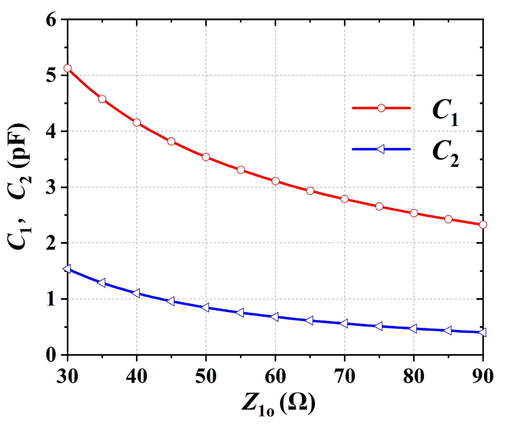
3. Design Procedures

In this section, a prototype was designed to validate the equations in Section 2. Detailed steps are listed below.
Step 1: Obtain the initial values of the circuit parameters.
In this design, the initial frequency f0 was assigned as 1.5 GHz, the impedances Zg and ZL were set as 50 Ω and (60 − j10) Ω, respectively. According to Equations (10) and (11), the curves of Z0e and Z0o versus θ0 can be plotted, as shown in Figure 3. Proper values of Z0e and Z0o can be determined by choosing θ0. Here, θ0 is chosen as 56°, Z0e = 138.3 Ω, and Z0o = 9.9 Ω. Substituting the obtained values in Equations (1) and (2), the values of Z1e and B are calculated by choosing a proper value of θ1. In the design, θ1 is selected as 60°, and the calculated values of Z1e and B are 127.4 Ω and −1.1 mS, respectively. From Equations (3) and (4), the curves of C1 and C2 versus different values of Z1o can be plotted, as shown in Figure 4. Here, the value of Z1o is selected as 80 Ω, and the initial values of C1 and C2 are calculated as 3.4 and 0.7 pF, separately.
Step 2: Obtain the corresponding values of C1, C2 and C3 when the frequency is tuned.
When the frequency was tuned from f0 to f1 with fixed terminal impedance ZL, the electrical length θ1 (60°) changed to θ1·f1/f0 (60°·f1/1.5 GHz). According to Equation (10), Y0e is a function of Zg, ZL, θ0. Substitute Equation (10) into Equation (1), and the novel value of θ0e (θ0) at f1 can be recalculated with the initial value of Z1e (Z1e = 127.4 Ω). The Z0o corresponding to the novel value of θ0 can be calculated by (11). Then, the novel values of B, C1, and C2 at f1 can be obtained using Equations (2)–(4). Figure 5 shows the curves of capacitor C1, C2, and C3 changing with the tuning frequency f1. It is seen that when the tuning frequency f1 is less than 1 GHz, the value of the capacitor C1 is less than 0 pF, which is unrealizable. Similarly, the value of C2 is less than 0 pF when the tuning frequency f1 is larger than 2.28 GHz. Thus, the theory frequency tuning range of the designed prototype is 1.0–2.28 GHz.
Table 1 shows the detailed calculated values of B, C1, and C2 corresponding to different tuning frequency f1 in consideration of the realizable capacitance. Because B is composed of an inductor L1 in parallel with a varactor C3, the values of C3 corresponding to different frequencies can be obtained with Equation (12) when choosing a fixed inductor. Here, L1 is chosen as 8.2 nH, and the corresponding values of C3 are illustrated in Table 1. In practice, the tuning fractional bandwidth of the proposed transformer is determined by the calculated realizable capacitance values of the three varactors.
Table 2 illustrates the circuit parameters obtained by the procedures of Steps 1 and 2. Based on the parameters, a model is established in ADS for simulation. The theory results are shown in Figure 6, which includes the tuning center frequencies of 1.1, 1.3, 1.5, 1.7, 1.9, and 2.1 GHz. It is observed that a frequency tuning range of 1.1–2.1 GHz (62.5%) is achieved by changing the values of C1, C2, and C3. In each tuning state, the |S11| is below −30 dB at the center frequency. Under the criterion of |S11| < −15 dB, the fractional bandwidths (FBWs) are 19.1%, 44.5%, 34.5%, 38.1%, 36.3%, 9.8%, respectively.
Step 3: Obtain the corresponding values of C1, C2, and C3 when the terminal impedance is tuned.
When the terminal impedance (ZL) is varied with fixed center frequency (f0 = 1.5 GHz), the novel value of θ0e (θ0) at f0 can also be recalculated with the initial value of Z1e (Z1e = 127.4 Ω) after substitute Equation (10) into Equation (1). The novel Z0o can also be obtained through Equation (11). Then, the novel values of C1, C2, and C3 can be obtained using Equations (2)–(4) and (12).
It is noted that for the determined Zg and ZL (RL + jXL), the range of its terminal complex impedance can be determined using the following limitations:
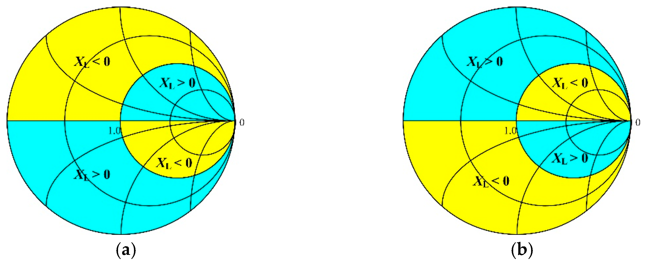
The initial impedance RL is larger than Zg:
(1)
When the real part of the transformed complex impedance is greater than Zg, the imaginary part has the same sign as XL.
(2)
When the real part of the transformed complex impedance is smaller than Zg, the imaginary part has the opposite sign to XL.
The initial impedance RL is smaller than Zg:
(1)
When the real part of the transformed complex impedance is smaller than Zg, the imaginary part has the same sign as XL.
(2)
When the real part of the transformed complex impedance is larger than Zg, the imaginary part has the opposite sign to XL.
Figure 7 shows the allowed and forbidden regions in the Smith chart according to the above limitations. The region which is colored yellow in Figure 7a corresponds to the situation of RL > Zg and XL < 0, whereas the blue region in Figure 7a is for RL > Zg and XL > 0. In Figure 7b, the blue and yellow regions represent the condition of RL > Zg/XL > 0 and RL > Zg/XL < 0, respectively.
For validation, several ZL examples were selected among the realizable impedance range shown in Figure 7. Table 3 illustrates the calculated C1, C2, and C3 values corresponding to different terminal impedances. The theory results are plotted in Figure 8. It is observed that the FBWs of 23.8%, 36.5%, 34.5%, 6.0%, and 4.6% are obtained when ZL equals with 80 − j30, 70 − j20, 60 − j10, 40 + j20, and 30 + j25 Ω, respectively, under the criterion of |S11| < −15 dB. At the center frequency, the |S11| is always below −28 dB.

4. Implementation and Measurements

To validate, the designed prototype was fabricated using the F4B substrate with a relative permittivity of 3.0, a loss tangent of 0.003, and a thickness of 1.5 mm. Figure 9 shows the layout and photograph of the fabricated prototype with an overall size of 35 mm × 24 mm. After optimization, the final dimensions were l1 = 5.6 mm, w1 = 0.95 mm, s1 = 1.0 mm, l2 = 6 mm, w2 = 3.76 mm, w3 = 1.5 mm, w4 = 1.2 mm, w5 = 1.5 mm, and the inductor L1 was 5.6 nH. The DC blocking capacitor Cblock was 33 μF, realized by Murata GRM-1885 series capacitors. Consider the variable capacitance C1, the SMV1281 from Skyworks Solutions, Inc., was utilized, which can provide a capacitance range of 0.69–13.3 pF with the bias voltage between 0 and 20 V. Similarly, for C2 and C3, the SMV2019 from Skyworks Solutions, Inc., was utilized, which can provide a capacitance range of 0.23–2.3 pF with the bias voltage between 0 and 20 V. The resistor Rbias with a value of 9.1 kΩ was used for biasing. Measurement results were obtained using an Agilent N5230A microwave network analyzer. The results for only frequency tunable, only impedance tunable, both frequency and impedance tunable are given.

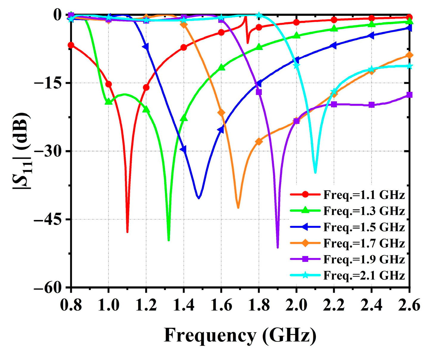
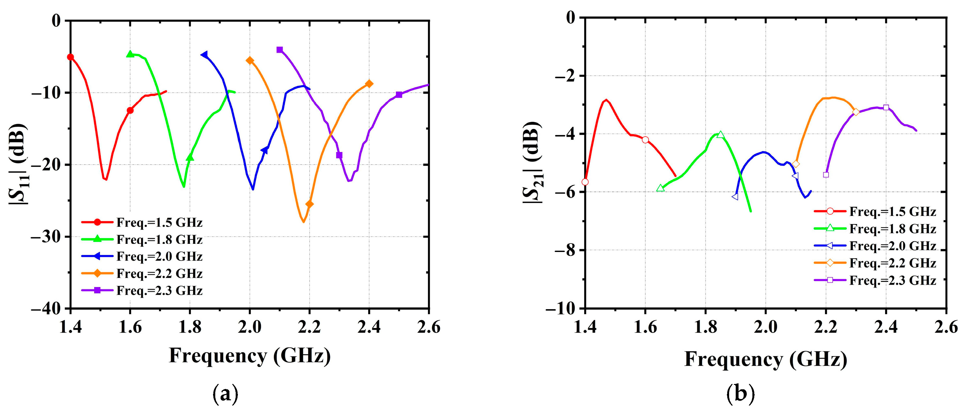
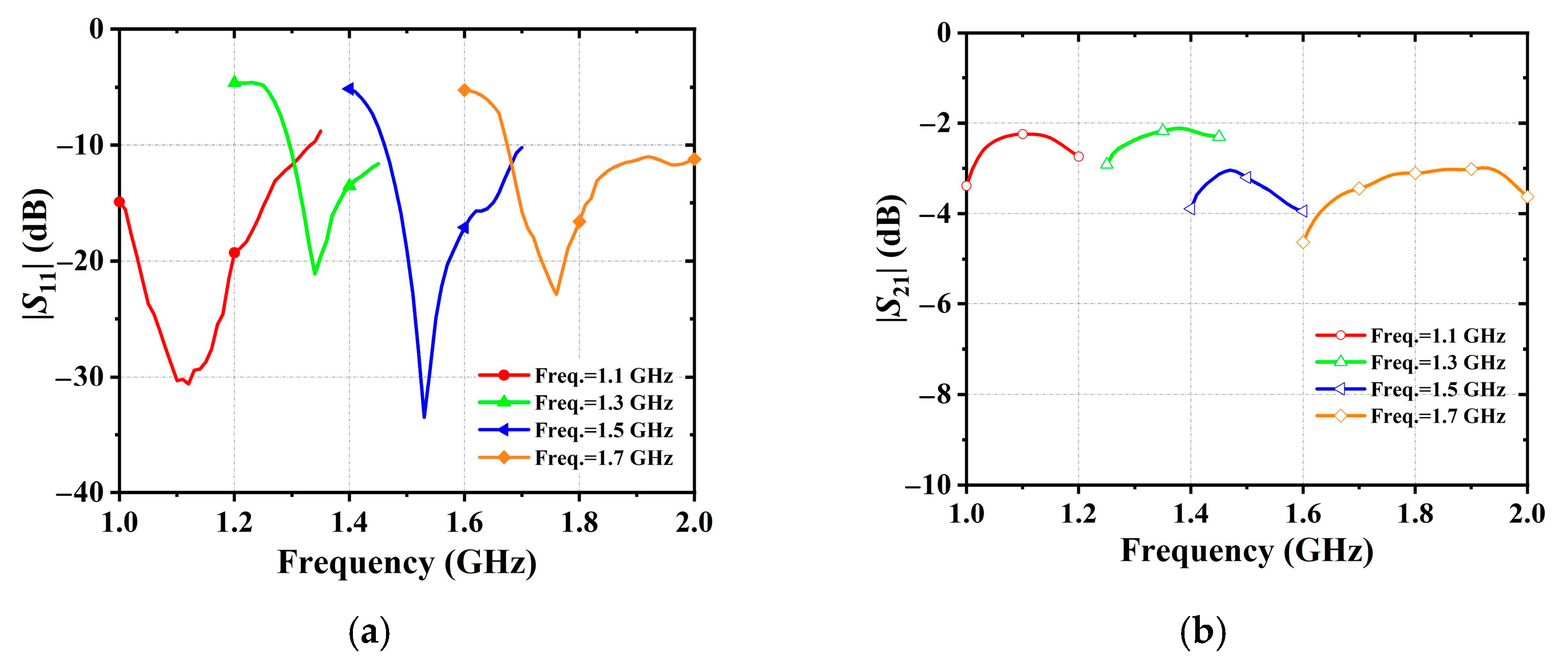
4.1. Frequency Tunable

Figure 10 plots the measurement results of different tuning frequencies under the bias voltage conditions shown in Table 4. The results indicate that the frequency of the fabricated prototype can be continuously adjusted from 1.1 to 2.1 GHz (62.5% tunability) by varying the bias voltages on the varactor diodes C1, C2, and C3 without changing the circuit dimensions. It is seen from Figure 10a that for 15 dB return loss, the measured FBWs are 5.0%, 7.7%, 9.8%, 15.9%, 14.3%, and 13.0% for the tuning center frequencies of 1.1, 1.3, 1.5, 1.7, 2.0, and 2.1 GHz, respectively. While at each tuning center frequency, the measured |S11| is less than −18 dB. As seen from Figure 10b, the measured insertion loss is in the range of 2–4 dB during the tuning of the frequency.

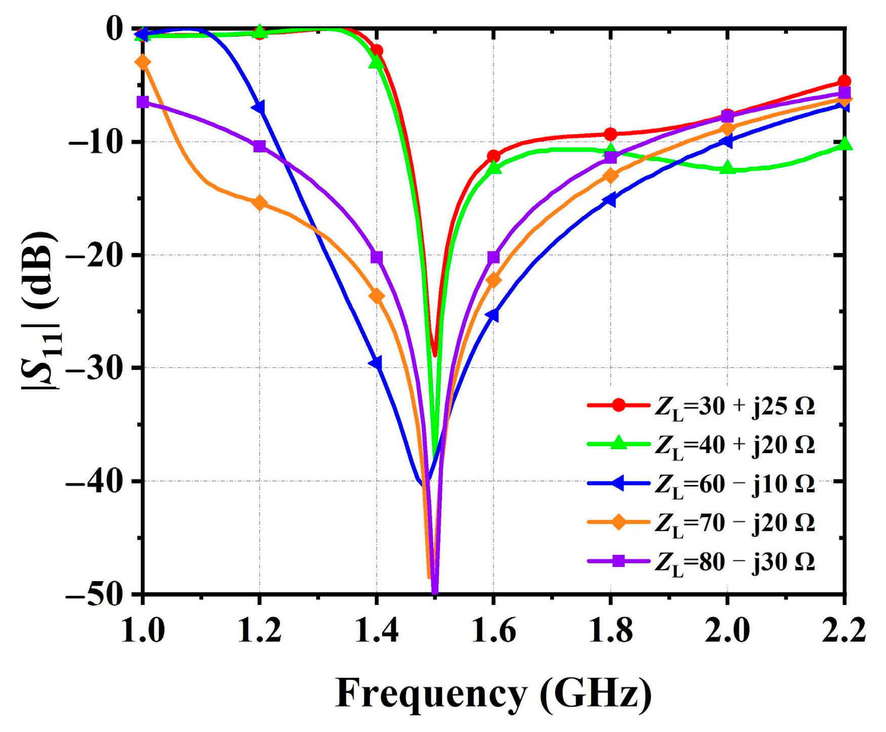
4.2. Terminal Impedance Tunable

Figure 11 plots the measurement results of different terminal impedances under the bias voltage conditions shown in Table 5. It is revealed that without changing the circuit dimensions, the terminal impedance of the designed CIT can be tuned by adjusting the bias voltages on the varactor. It is observed from Figure 11a that for each terminal impedance, the measured |S11| at the center frequency is less than −20 dB. While under the criterion of |S11| < −15 dB, the measured FBWs are 5.3%, 10.0%, 15.9%, and 10.3% for ZL equals with 35 + j25 Ω, 40 + j20 Ω, 60 − j10 Ω, and 75 − j15 Ω, respectively. During the tuning, the measured |S21| was in the range of −3 dB–−4.2 dB, as shown in Figure 11b.

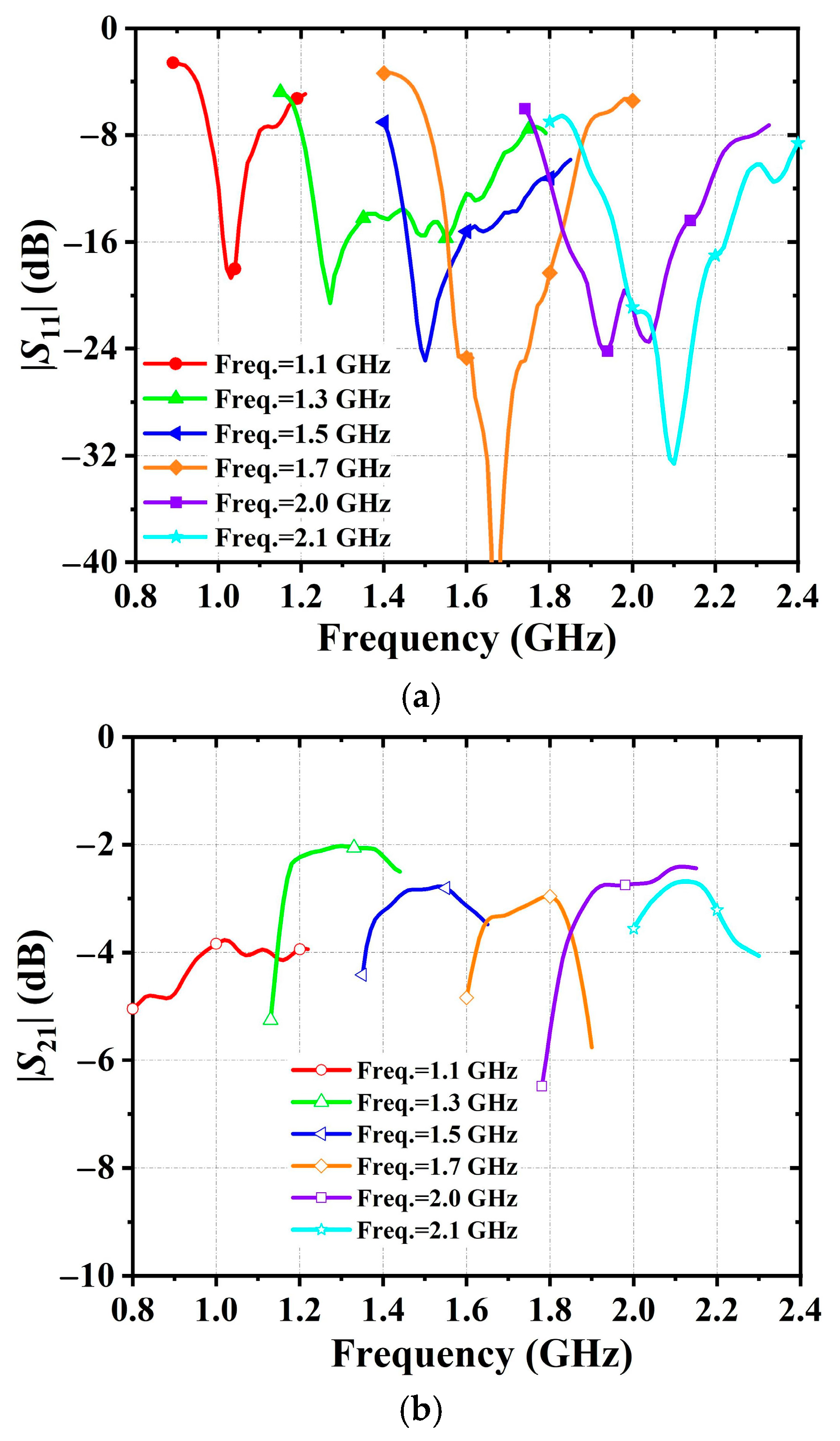
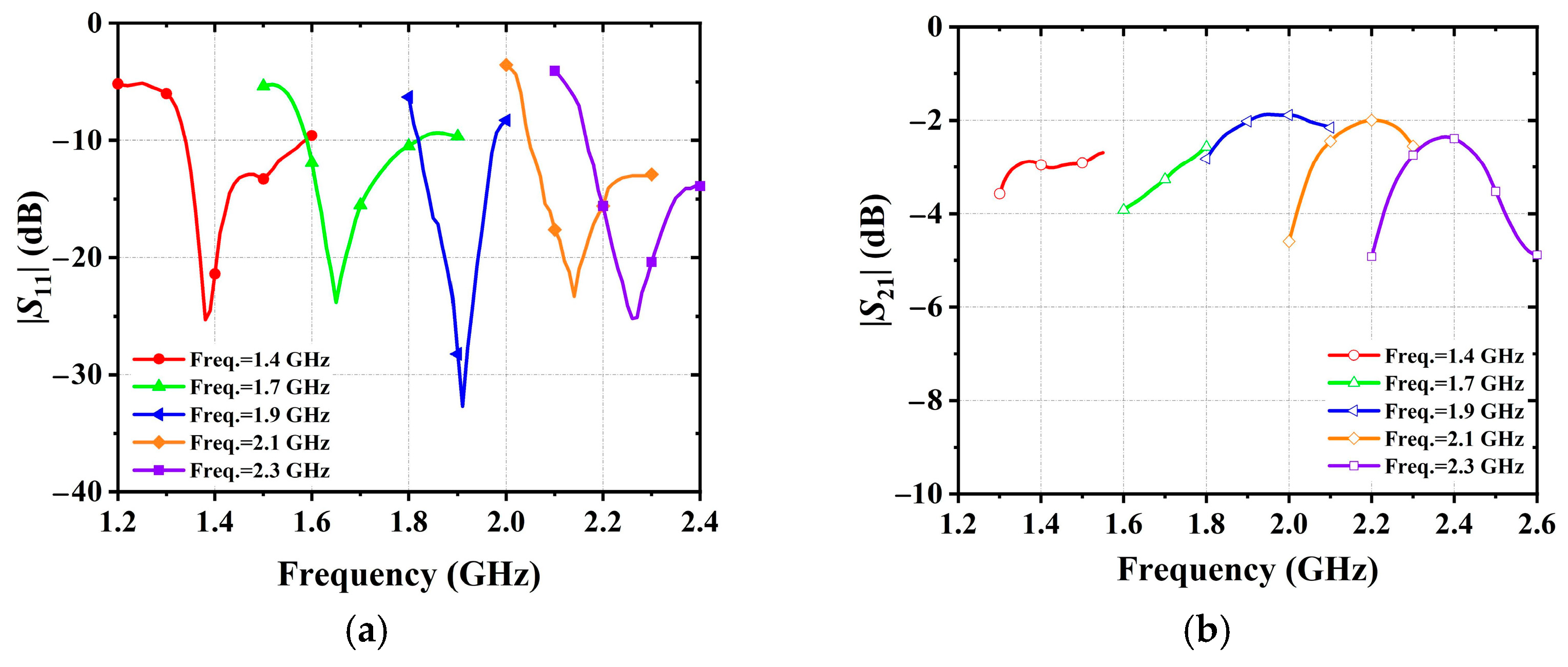
4.3. Both Frequency and Terminal Impedance Tunable

Figure 12, Figure 13, Figure 14 and Figure 15 show the measurement results of different tuning frequencies corresponding to four different terminal impedances (ZL = (35 + j25) Ω, (40 + j20) Ω, (75 − j15) Ω, and (80 − j30) Ω) under the bias voltage conditions shown in Table 6. As seen from Figure 10, the measured frequency tuning range is from 1.5 GHz to 2.3 GHz (42.1%) when the terminal impedance is changed to (35 + j25) Ω. During the tuning, the FBWs are in the range of 5.2–7.7% under 15 dB return loss.
At each tuning center frequency, the measured |S11| is less than −20 dB with less than 5 dB insertion loss. When the terminal impedance is tuned to (40 + j20) Ω, the frequency can be tuned from 1.3 GHz to 2.2 GHz (51.4%) with more than 20 dB return loss and less than 4 dB insertion loss at each tuning center frequency. In addition, the measured FBWs for |S11| < −15 dB are in the range of 5.1–9.3%. For ZL = (75 − j15) Ω and (80 − j30) Ω, the measured tuning center frequencies are in the range of 1.1–1.7 GHz (42.9%), and 1.4–2.3 GHz (48.6%), respectively. At each tuning center frequency, the measured return losses are more than 20 dB return loss and the measured insertion losses are less than 3.5 dB.
Table 7 summarizes the performance comparisons among the proposed and reported representative CITs. In Zhang et al. [18], the CIT was operated at two certain frequencies. For the CITs in EI-Nozahi et al. [17] and Lee and Lin [19], the frequency was tuned continuously with fixed terminal impedance. However, the tunability was less than 50%. In references [19,20,21,23,27,28], the terminal impedance was reconfigured at a certain fixed center frequency. Due to the using of switch diodes, the changing of terminal impedance was discrete. By using ferroelectric capacitors [24] and varactors [25,26], the terminal impedance can be tuned continuously. Although the work in [22] showed a frequency and impedance tuning ability, the bandwidth was narrow (<2%). d with the reported work, the proposed CIT exhibited higher flexibility including a larger frequency tuning range of 62.5% and a continuous tuning of the terminal impedance with enhanced bandwidth (>5%). The insertion loss of the designed prototype was slightly higher than other structures. Because a high Q-factor corresponds to low insertion loss, the loss of the CIT can be reduced by choosing varactors with a high Q-factor. In summary, the progress of the proposed CIT indicates that it can serve as a good candidate for microwave applications.

5. Conclusions

In this paper, a compact CIT with tunable frequency and terminal impedance was presented. The tunable characteristic was achieved by changing the capacitance of the three types of varactors shunt on the coupled lines. To demonstrate, an example was designed and fabricated. The measurement results verified the functions, including only frequency tunable, only terminal impedance tunable, and both frequency and terminal impedance tunable. The progress of the proposed structure indicates that it has the potential for applications in radio frequency front-end and monolithic microwave integrated circuits.

Author Contributions

Conceptualization, H.L. and Y.G.; methodology, H.L. and Y.G.; software, X.W.; validation, S.F. and Z.W.; formal analysis, H.L. and Y.G.; investigation, X.W.; resources, H.L., S.F. and Z.W.; data curation, S.F. and Z.W.; writing—original draft preparation, Y.G.; writing—review and editing, H.L.; visualization, X.W.; supervision, Z.W.; project administration, S.F.; funding acquisition, H.L. and Z.W. All authors have read and agreed to the published version of the manuscript.

Funding

This work is supported in part by the National Natural Science Foundation of China under Grant 51809030 and Grant 61871417, in part by the Natural Science Foundation of Liaoning Province under Grant 2020-MS-127, in part by the Liaoning Revitalization Talents Program under Grant XLYC2007067, and in part by the Dalian Youth Science and Technology Star Project under Grant 2020RQ007.

Data Availability Statement

All data are included within manuscript.

Conflicts of Interest

The authors declare no conflict of interest.

Appendix A

Figure A1 and Figure A2 show the subcircuits of the proposed CIT and the equivalent parallel coupled line using the even–odd mode analysis, respectively.
Figure A1. Subcircuits of the proposed CIT. (a) Even–even mode. (b) Even–odd mode. (c) Odd–even mode. (d) Odd–odd mode.
Electronics 11 00983 g0a1
Figure A2. Subcircuits of the equivalent parallel coupled line. (a) Even–even mode. (b) Even–odd mode. (c) Odd–even mode. (d) Odd–odd mode.
Electronics 11 00983 g0a2
According to Figure A1, the port admittances (Yee, Yeo, Yoe, and Yoo) of the subcircuits for the proposed CIT can be expressed, as listed in Equations (A1)–(A4).
Y ee = j Y 1 e Y 1 e tan θ 1 e 2 + B 2 Y 1 e B 2 tan θ 1 e 2
Y eo = j Y 1 e cot θ 1 e 2
Y oe = j Y 1 o Y 1 o 2 π f 1 C 2 + B 2 + Y 1 o tan θ 1 o 3 Y 1 o 2 π f 1 C 2 + B 2 tan θ 1 o 3 + 4 π f 1 C 1 + Y 1 o tan θ 1 o 6 Y 1 o Y 1 o 2 π f 1 C 2 + B 2 + Y 1 o tan θ 1 o 3 Y 1 o 2 π f 1 C 2 + B 2 tan θ 1 o 3 + 4 π f 1 C 1 tan θ 1 o 6
Y oo = j Y 1 o Y 1 o tan θ 1 o 6 + 4 π f 1 C 1 Y 1 o cot θ 1 o 3 Y 1 o + Y 1 o cot θ 1 o 3 4 π f 1 C 1 tan θ 1 o 6
According to Figure A2, the port admittances (Y1ee, Y1eo, Y1oe, and Y1oo) of the subcircuits for the equivalent parallel coupled line can be expressed, as listed in Equation (A5) and (A6).
Y 1 ee = j Y 0 e tan θ 0 e 2 · Y 1 eo = j Y 0 e cot θ 0 e 2
Y 1 oe = j Y 0 o tan θ 0 o 2 · Y 1 oo = j Y 0 o cot θ 0 o 2
Because the parallel coupled line is equivalent with the proposed CIT, Yij = Y1ij (i, j = e or o). Then, the relations of Equations (1)–(4) can be derived.

References

  1. Tsao, Y.-F.; Würfl, J.; Hsu, H.-T. Bandwidth Improvement of MMIC Single-Pole-Double-Throw Passive HEMT Switches with Radial Stubs in Impedance-Transformation Networks. Electronics 2020, 9, 270. [Google Scholar] [CrossRef] [Green Version]
  2. Kim, H.-W.; Ahn, M.; Lee, O.; Kim, H.; Kim, H.; Lee, C.-H. Analysis and Design of a Fully-Integrated High-Power Differential CMOS T/R Switch and Power Amplifier Using Multi-Section Impedance Transformation Technique. Electronics 2021, 10, 1028. [Google Scholar] [CrossRef]
  3. Ali, E.M.; Alibakhshikenari, M.; Virdee, B.S.; Soruri, M.; Limiti, E. Efficient Wireless Power Transfer via Magnetic Resonance Coupling Using Automated Impedance Matching Circuit. Electronics 2021, 10, 2779. [Google Scholar] [CrossRef]
  4. Lu, Z.; Zhao, Y.; Liu, D. Adaptive Impedance Matching Scheme for Magnetic MIMO Wireless Power Transfer System. Electronics 2021, 10, 2788. [Google Scholar] [CrossRef]
  5. Ahn, H.-R.; Tentzeris, M.M. Complex impedance transformers based on allowed and forbidden regions. IEEE Access 2019, 7, 39288–39298. [Google Scholar] [CrossRef]
  6. Manoochehri, O.; Asoodeh, A.; Forooraghi, K. Π-model dual-band impedance transformer for unequal complex impedance loads. IEEE Microw. Compon. Lett. 2015, 25, 238–240. [Google Scholar] [CrossRef]
  7. Chuang, M.; Wu, M. General dual-band impedance transformer with a selectable transmission zero. IEEE Trans. Compon. Packag. Manufact. Technol. 2016, 6, 1113–1119. [Google Scholar] [CrossRef]
  8. Xie, T.; Wang, X.; Ma, Z.; Chen, C.-P.; Lu, G. A novel analysis approach for dual-frequency parallel transmission-line transformer with complex terminal loads. IEEE Access 2020, 8, 57472–57482. [Google Scholar] [CrossRef]
  9. Chen, M.-G.; Hou, T.-B.; Tang, C.-W. Design of planar complex impedance transformers with the modified coupled line. IEEE Trans. Compon. Packag. Manufact. Technol. 2012, 2, 1704–1710. [Google Scholar] [CrossRef]
  10. Fang, S.; Jia, X.; Liu, H.; Wang, Z. Design of compact coupled-line complex impedance transformers with the series susceptance component. IEEE Trans. Circuits Syst. II Express Br. 2020, 67, 2482–2486. [Google Scholar] [CrossRef]
  11. Lu, P.; Yang, X.S.; Li, J.L.; Wang, B.Z. Polarization reconfigurable broadband rectenna with tunable matching network for microwave power transmission. IEEE Trans. Antennas Propag. 2016, 64, 1136–1141. [Google Scholar] [CrossRef]
  12. Fu, J.-S.; Mortazawi, A. Improving power amplifier efficiency and linearity using a dynamically controlled tunable matching network. IEEE Trans. Microw. Theory Techn. 2008, 56, 3239–3244. [Google Scholar]
  13. Neo, W.C.E.; Lin, Y.; Liu, X.-D.; De Vreede, L.C.N.; Larson, L.E.; Spirito, M.; Pelk, M.J.; Buisman, K.; Akhnoukh, A.; De Graauw, A.; et al. Adaptive multi-band multi-mode power amplifier using integrated varactor-based tunable matching networks. IEEE J. Solid State Circuits 2006, 41, 2166–2176. [Google Scholar] [CrossRef]
  14. Ko, C.-H.; Rebeiz, G.M. A 1.4–2.3 GHz tunable diplexer based on reconfigurable matching networks. IEEE Trans. Microw. Theory Techn. 2015, 63, 1595–1602. [Google Scholar] [CrossRef]
  15. Vaha-Heikkila, T.; Lahdes, M.; Kantanen, M.; Tuovinen, J. On-wafer noise-parameter measurements at W-band. IEEE Trans. Microw. Theory Techn. 2003, 51, 1621–1628. [Google Scholar] [CrossRef]
  16. McIntosh, C.E.; Pollard, R.D.; Miles, R.E. Novel MMIC source-impedance tuners for on-wafer microwave noise-parameter measurements. IEEE Trans. Microw. Theory Techn. 1999, 47, 125–131. [Google Scholar] [CrossRef]
  17. MI-Nozahi, E.; Sanchez-Sinencio, E.; Entesari, K. A CMOS low noise amplifier with reconfigurable input matching network. IEEE Trans. Microw. Theory Techn. 2009, 57, 1054–1062. [Google Scholar] [CrossRef]
  18. Zhang, H.; Gao, H.; Li, G.-P. Broad-band power amplifier with a novel tunable output matching network. IEEE Trans. Microw. Theory Tech. 2005, 53, 3606–3614. [Google Scholar] [CrossRef]
  19. Lee, C.I.; Lin, W.C. A novel p-i-n inductor for tunable wideband matching network application. IEEE Trans. Electron Devices 2013, 60, 2611–2618. [Google Scholar] [CrossRef]
  20. Sanchez-Perez, C.; de Mingo, J.; Carro, P.L.; García-Dúcar, P. Design and applications of a 300–800 MHz tunable matching network. IEEE J. Emerg. Sel. Top. Circuits Syst. 2013, 3, 531–540. [Google Scholar] [CrossRef]
  21. Fouladi, S.; Domingue, F.; Zahirovica, N.; Mansour, R.R. Distributed MEMS tunable impedance-matching network based on suspended slow-wave structure fabricated in a standard CMOS technology. IEEE Trans. Microw. Theory Tech. 2010, 58, 1056–1064. [Google Scholar] [CrossRef]
  22. Hoarau, C.; Corrao, N.; Arnould, J.-D.; Ferrari, P.; Xavier, P. Complete Design and Measurement Methodology for a Tunable RF Impedance-Matching Network. IEEE Trans. Microw. Theory Tech. 2008, 56, 2620–2627. [Google Scholar] [CrossRef]
  23. Brito, K.; de Lima, R.N. Tunable impedance matching network. In Proceedings of the 2007 SBMO/IEEE MTT-S International Microwave and Optoelectronics Conference, Salvador, Brazil, 29 October–1 November 2007; pp. 117–121. [Google Scholar]
  24. Tombak, A. A Ferroelectric-Capacitor-Based Tunable Matching Network for Quad-Band Cellular Power Amplifiers. IEEE Trans. Microw. Theory Tech. 2007, 55, 370–375. [Google Scholar] [CrossRef]
  25. Arabi, E.; Morris, K.A.; Beach, M.A. Analytical Formulas for the Coverage of Tunable Matching Networks for Reconfigurable Applications. IEEE Trans. Microw. Theory Tech. 2017, 65, 3211–3220. [Google Scholar] [CrossRef] [Green Version]
  26. Shen, Q.; Barker, N.S. Distributed MEMS tunable matching network using minimal-contact RF-MEMS varactors. IEEE Trans. Microw. Theory Tech. 2006, 54, 2646–2658. [Google Scholar] [CrossRef]
  27. Jeong, H.T.; Kim, J.E.; Chang, I.S.; Kim, C.D. Tunable impedance transformer using a transmission line with variable characteristic impedance. IEEE Trans. Microw. Theory Tech. 2005, 53, 2587–2593. [Google Scholar] [CrossRef]
  28. Suvarna, A.R.; Bhagavatula, V.; Rudell, J.C. Transformer-Based Tunable Matching Network Design Techniques in 40-nm CMOS. IEEE Trans. Circuits Syst. II Express Br. 2016, 63, 658–662. [Google Scholar] [CrossRef]
  29. Jensen, T.; Zhurbenko, V.; Krozer, V.; Meincke, P. Coupled transmission lines as impedance transformer. IEEE Trans. Microw. Theory Tech. 2007, 55, 2957–2965. [Google Scholar] [CrossRef] [Green Version]
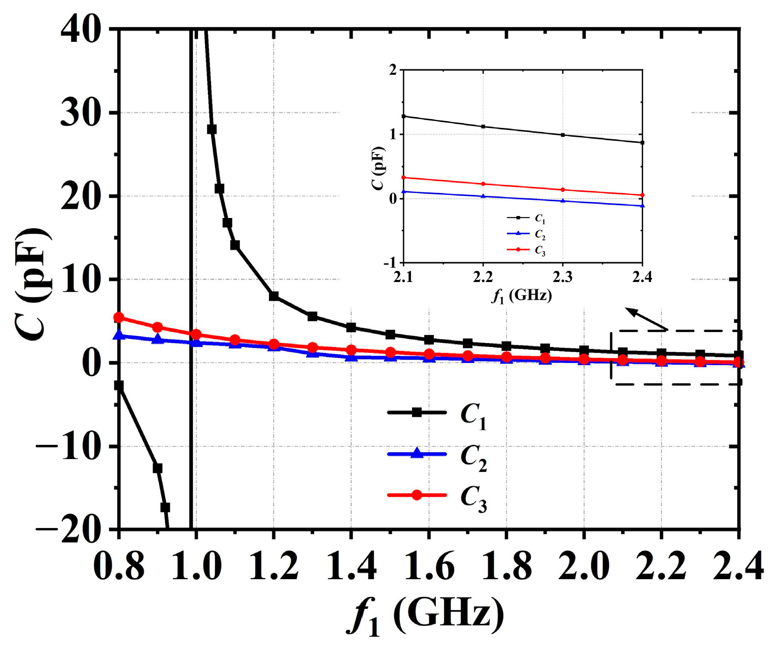
Figure 1. Schematic of the proposed tunable CIT.
Electronics 11 00983 g001
Figure 2. Equivalent circuit of the parallel susceptance.
Electronics 11 00983 g002
Figure 3. Curves of Z0e and Z0o versus θ0.
Electronics 11 00983 g003
Figure 4. Curves of C1 and C2 versus Z1o.
Electronics 11 00983 g004
Figure 5. Curves of C1, C2 and C3 versus f1.
Electronics 11 00983 g005
Figure 6. Theory results for different tuning frequencies f1.
Electronics 11 00983 g006
Figure 7. Allowed and forbidden regions for the tuning impedances. (a) RL > Zg; (b) RL < Zg.
Electronics 11 00983 g007
Figure 8. Theory results for different terminal impedance ZL.
Electronics 11 00983 g008
Figure 9. (a) Layout and (b) photograph of the designed prototype.
Electronics 11 00983 g009
Figure 10. Measured (a) |S11| and (b) |S21| of the designed CIT with only tuning frequency.
Electronics 11 00983 g010
Figure 11. Measured (a) |S11| and (b) |S21| of the designed CIT with only terminal impedance tunable.
Electronics 11 00983 g011
Figure 12. Measured (a) |S11| and (b) |S21| of the designed CIT for ZL = 30 + j25 Ω.
Electronics 11 00983 g012
Figure 13. Measured (a) |S11| and (b) |S21| of the designed CIT for ZL = 40 + j20 Ω.
Electronics 11 00983 g013
Figure 14. Measured (a) |S11| and (b) |S21| of the designed CIT for ZL = 75 − j15 Ω.
Electronics 11 00983 g014
Figure 15. Measured (a) |S11| and (b) |S21| of the designed CIT for ZL = 80 − j30 Ω.
Electronics 11 00983 g015
Table 1. Calculated values of B, C1, C2, and C3 corresponding to different tuning frequency f1.
f1 (GHz)C1 (pF)C2 (pF)B (mS)C3 (pF)
1.113.82.21.32.7
1.35.50.20.11.8
1.53.40.7−1.11.3
1.72.30.5−2.30.9
1.91.70.3−3.60.6
2.11.20.2−4.90.3
Table 2. Parameters of the designed tune impedance transformer.
Zg (Ω)50Z1o (Ω)80
ZL (Ω)60–j10θ1 (°)60
f0 (GHz)1.5L1 (nH)8.2
Z0e (Ω)138.3f1 (GHz)1.1–2.1
Z0o (Ω)9.9C1 (pF)1.2–13.8
θ0 (°)56C2 (pF)0.2–2.2
Z1e (Ω)127.4C3 (pF)0.3–2.7
Table 3. Calculated values of C1, C2, and C3 corresponding to different terminal impedance ZL.
ZL (Ω)C1 (pF)C2 (pF)C3 (pF)
80 − j307.880.991.22
70 − j204.411.011.24
60 − j103.400.701.30
40 + j202.330.800.99
30 + j252.320.821.23
Table 4. Bias conditions for different tuning frequencies.
Freq. (GHz)Biasing Conditions
1.1V1 = 1.3 V, V2 = 2.7 V, V3 = 1.1 V
1.3V1 = 2.7 V, V2 = 4.1 V, V3 = 2.2 V
1.5V1 = 4.4 V, V2 = 5.0 V, V3 = 3.7 V
1.7V1 = 7.1 V, V2 = 7.3 V, V3 = 6.4 V
2.0V1 = 9.4 V, V2 = 8.6 V, V3 = 8.5 V
2.1V1 = 12.9 V, V2 = 10.2 V, V3 = 12.6 V
Table 5. Bias conditions for different terminal impedances.
ZL (Ω)Biasing Conditions
35 + j25V1 = 5.5 V, V2 = 4.7 V, V3 = 1.8 V
40 + j20V1 = 5.2 V, V2 = 6.4 V, V3 = 1.8 V
60 − j10V1 = 4.4 V, V2 = 5.0 V, V3 = 3.7 V
75 − j15V1 = 5.4 V, V2 = 5.8 V, V3 = 4.4 V
Table 6. Bias conditions for different tuning frequencies and terminal impedances.
ZL (Ω)Freq. (GHz)Biasing Conditions (V)
35 + j251.5V1 = 5.5, V2 = 4.7, V3 = 1.8
1.8V1 = 7.1, V2 = 5.8, V3 = 3.1
2.0V1 = 8.7, V2 = 7.2, V3 = 4.4
2.2V1 = 10.6, V2 = 8.5, V3 = 5.8
2.3V1 = 13.2, V2 = 10.0, V3 = 7.6
40 + j201.3V1 = 3.9, V2 = 4.6, V3 = 0.9
1.5V1 = 5.2, V2 = 6.4, V3 = 1.8
1.8V1 = 6.7, V2 = 7.1, V3 = 3.1
2.1V1 = 8.2, V2 = 8.7, V3 = 4.4
2.2V1 = 9.6, V2 = 12.4, V3 = 6.1
75 − j151.1V1 = 1.7, V2 = 3.4, V3 = 1.5
1.3V1 = 3.5, V2 = 4.4, V3 = 2.7
1.5V1 = 5.4, V2 = 5.8, V3 = 4.4
1.7V1 = 6.8, V2 = 7.2, V3 = 5.9
80 − j301.4V1 = 4.7, V2 = 6.4, V3 = 4.9
1.7V1 = 6.2, V2 = 8.0, V3 = 6.9
1.9V1 = 8.4, V2 = 9.9, V3 = 10.7
2.1V1 = 10.6, V2 = 12.2, V3 = 13.8
2.3V1 = 11.9, V2 = 13.6, V3 = 16.0
Table 7. Performance comparisons among the proposed and reported representative CITs.
Ref.TechnologyTuningInsertion Loss
FrequencyImpedance
[17]Tunable inductorΔf/f0 = 23.3%
(Continuous)
NO--
[18]Pin diodes0.9 GHz, 2.0 GHzNO--
[19]Pin inductor at RF breakdownΔf/f0 = 44.4%
(Continuous)
YES
(Discrete)
2–3.5 dB
[20]Pin diodesNOYES
(Discrete)
--
[21]Switched MEMS capacitorsNOYES
(Discrete)
0.4–7.55 dB
[22]VaractorΔf/f0 = 50%
(Continuous)
YES
(Continuous)
2.5–3.5 dB
[23]MEMS-based switchesNOYES
(Discrete)
0.7–2.1 dB
[24]Ferroelectric capacitorsNOYES
(Continuous)
1.4–2.5 dB
[25]VaractorNOYES
(Continuous)
--
[26]RF-MEMS
varactors
NOYES
(Continuous)
2.5–5 dB
[27]Pin diodesNOYES
(Discrete)
About 0.2 dB
[28]NMOS switchesNOYES
(Discrete)
1.8–4 dB
This workVaractorΔf/f0 = 62.5%
(Continuous)
YES
(Continuous)
2–4.5 dB
Publisher’s Note: MDPI stays neutral with regard to jurisdictional claims in published maps and institutional affiliations.

