Abstract
In response to the issue of large input current ripple and noise, which can cause current shocks and compromise the overall stability in single-tube wireless power transmission systems, a P# type LCC-S compensation network and a multi-coil phase-shifting control method have been proposed to suppress input current ripple, improve input current waveform, reduce input current total harmonic distortion (THD), and ultimately enhance system efficiency and stability. Firstly, the working mode and waveform of the P# type LCC-S compensation network are analyzed, and the calculation method for its parameters is provided. Secondly, the analytical relationship between input current, input voltage, coil mutual inductance, and load impedance of the multi-coil array is derived. Additionally, Fourier transform is used to analyze the input current composition, and the phase shift suppression method is employed to reduce the input current ripple. Finally, a test platform is constructed to verify the relevant experiments. The experimental results demonstrate that the input current ripple is significantly suppressed at the rated transmission power, and the system efficiency is improved to 88.2%, which validates the effectiveness of the proposed method.
1. Introduction
Wireless power transfer (WPT) technology enables energy to be transmitted through an air gap without physical contact [1,2,3,4,5]. Due to its advantages of safety, convenience, and flexibility, it is the best choice for charging, in place of cables [6,7,8]. Consequently, it has been widely used in the power supply of consumer electronics, electric cars, special machinery, and medical electronics [9,10].
In the research of wireless power transfer technology, the research on multi-coil parallel transmission is mostly based on full-bridge or half-bridge topology [11,12,13,14,15,16]. However, these topologies have some problems, such as complex peripheral circuits and the risk of short circuits on one arm of the inverter bridge [17,18,19,20,21]. In contrast, the single-switch resonant inverter circuit has the advantages of high reliability, simple control, and low cost, and it is easy to realize zero-voltage turn-on, but it has some disadvantages such as limited transmission power and large input current ripple. Therefore, by connecting multiple transmitters in parallel and controlling the angle of the input current of the system, the conducting ripple is suppressed and the transfer power is increased. It is an effective way to overcome the deficiency of a single-switch resonant inverter. Under the same transfer power, the control scheme of the system is simpler than the full-bridge topology. A master–slave phase parallel inverter topology with phase synchronization control is proposed by [22], but the auxiliary inverter is only used for tuning. In reference [23], a WPT system with input parallel and output series topology based on a full-bridge inverter is proposed, along with an efficiency optimization method. The efficiency of the single-switch LCC-S compensation network was optimized, resulting in an output power of 11 W and efficiency of 86.3% [24]. SiC MOSFET is used in wireless power transfer circuits based on a single-switch PP resonant inverter, which effectively improves the system efficiency, but the input current alignment of the system is not considered [25].
Due to the unique characteristics of the single-switch resonant inverter wireless power transfer system, the conventional LCC resonant topology cannot be directly applied. The compensation network of a single-switch resonant inverter transmitter typically features a P-type structure. The resonant frequency of PP-type and PS-type circuits is determined by the transmitter’s Lt, the receiver’s Lr, the mutual inductance M, and the load RL [26].
LCC topology has the following advantages:
- a.
- The compensation network parameters can be adjusted to achieve constant voltage output for the system.
- b.
- The resonant frequency of the system is only related to the transmitter and receiver which are not affected by the change in mutual inductance or load, which will not be detuned easily when the system works.
- c.
- The LCC topology has a high-quality index of merit as a high-order network and a good filtering effect on high harmonics. The voltage gain is adjustable, and it requires a low input voltage level.
However, when the magnetic coupler shifts, the mutual inductance M changes, which can significantly alter the resonant frequency and ultimately impact the transmission power and efficiency of the WPT system. Additionally, P-type compensation networks have low voltage gains and a low figure of merit. At high input voltages, the filtering effect of the system is also poor. To summarize, the main contributions are as follows:
- (1)
- To improve the THD of the system’s input current, the working modes and parameters of different resonant circuits are analyzed, and the P# type LCC-S compensation network is determined. We suggest a P# type LCC-S compensation network suitable for single-switch resonant inverter, specifically for multi-coil single-switch wireless power transfer.
- (2)
- To improve the transmission power of the system, three coils are input in parallel to increase the transmission power of the system. Aiming at the topology of three-coil parallel input, Fourier expansion analysis is carried out to obtain the mathematical model of three-coil compensation network.
- (3)
- To suppress the ripple of the input current, the effective values of the fundamental and harmonic components are obtained through a frequency domain analysis of the input current. Meanwhile, the relationship between the input current of the coil and input voltage, coil mutual inductance and negative load impedance under the unbalanced coupling of three turns is deduced. In view of the topology of the three-coil parallel input, the input current ripple is suppressed using the method of phase shift control. The system efficiency is improved.
2. System Structure and Operation Process
2.1. The Circuit Model of Triple-Coil Single-Switch Resonant Inverter WPT System
The construction and dimensions of the three-coil WPT system are shown in Figure 1. The distance between the transmitter and the receiver is 50 mm. The length and width of the ferrite are 160 mm, and the thickness is 2 mm. The magnetic coupler is wound with 0.1 mm × 150 strand litz wire.
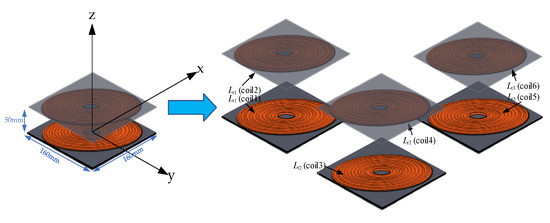
Figure 1.
Three-coil WPT system.
The circuit construction of the system is shown in Figure 2. Vdc is the input DC voltage of the single-switch resonant inverter; Q1~Q3 is the power MOSFET; Lf1~Lf3 is the transmitter compensation inductance; Cf1~Cf3 is the transmitter parallel compensation capacitor; Lt1~Lt3 is the transmitter; Ct1~Ct3 is the transmitter series compensation capacitor; Lf1~Lf3, Cf1~Cf3, Ct1~Ct3, and Lt1~Lt3, respectively, constitute the LCC compensation circuit at the transmitter; Rt1~Rt3 is the parasitic resistance of the transmitter; La1~La3 is the resonant inductor; Ca1~Ca3 is the resonant capacitor; M1~M3 is the mutual inductance between the magnetic coupler; Lr1~Lr3 is the receiver; Rr1~Rr3 is the parasitic resistance of the receiver; Cr1~Cr3 is the compensation capacitor of the receiver; D1~D3 is the rectifier; CL1~CL3 is the output filter capacitor; and RL is the load resistance. Iin1~Iin3 is the input current of each inverter; i1~i3 is the compensation inductance current at the transmitter; it1~it3 is the excitation current of the transmitter; ir1~ir3 is the output current of the receiver; vo1~vo3 is the input voltage of the rectifier; IL is the load current; and VL is the load voltage.
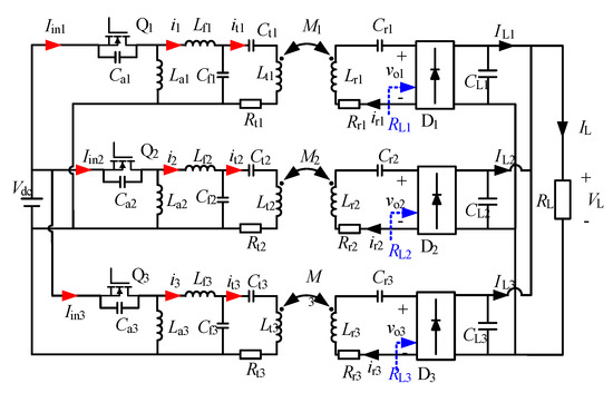
Figure 2.
The WPT system with three parallel-connected coils.
2.2. Analysis of Circuit Model Operation Mode of Three Groups of Single-Switch Resonant Inverter WPT System
Because of the particularity of the single-switch resonant inverter, the conventional LCC resonant network cannot be directly applied. It is possible to add an additional LC resonance circuit at the transmitter for resonance, and the LCC compensation network is used as the compensation circuit, as shown in Figure 3a. So, the single-switch resonant inverter has the characteristics of an LCC compensation network. In addition, the LC resonant circuit also plays a role in adjusting the zero-voltage switching margin (ZVSM). However, the system input current of the traditional single-switch LCC compensation network is seriously distorted, as shown in Figure 4a.
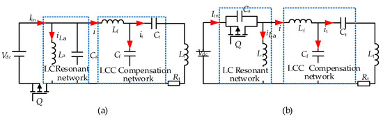
Figure 3.
LCC resonant network based on single-switch resonance inverter. (a) Traditional single-tube resonant inverter LCC compensation network. (b) P# single-tube resonant inverter LCC compensation network.
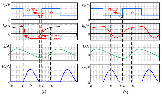
Figure 4.
Comparison of operating modal waveforms of two compensation networks. (a) Traditional single-tube resonant inverter LCC compensates network operating mode waveform. (b) P# single-tube resonant inverter LCC compensates network operating mode waveform.
Therefore, based on the traditional LCC compensation network, this paper proposes a P# type LCC compensation network suitable for the single-switch resonant inverter, as shown in Figure 3b. The resonant capacitor Ca of this circuit is connected in parallel with the MOSFET to transfer the current oscillation at the input of the system to the ground, as shown in Figure 4b, which effectively improves the system input current waveform, reduces the THD of the system input current, and improves the system efficiency.
As shown in Figure 2, the compensation network can be divided into an LC resonance network and an LCC compensation network. For the convenience of analysis, it is assumed that all components in the circuit are ideal components. The system operating mode waveforms of different compensation networks are shown in Figure 4. Vgs is the driving voltage of the MOSFET. iLa is the resonant inductance current, i is the compensation inductance current at the transmitter, and Vds is the voltage between the drain and source of the MOSFET.
As shown in Figure 4 and Table 1, the status of a single period for two different LCC resonant topologies. As can be seen from Figure 4 and Figure 5, the operating difference of the two different compensation networks is only reflected in the input current. When the traditional LCC compensation network works, its input current Iin has large higher harmonics, and the process of phase shifting to suppress the fundamental and lower harmonics will cause the superposition of higher harmonics, so the LCC compensation network is not suitable for phase shifting to suppress the input current. However, the P# type LCC compensation network eliminates the high-order harmonics in the input current Iin and reduces the THD of the input current, so it is suitable for the phase-shifting suppression of the input current.

Table 1.
Modal analysis of the transmitter.
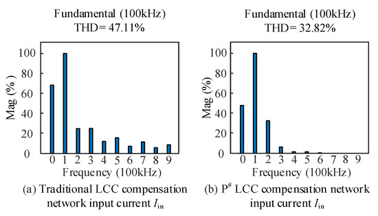
Figure 5.
Comparison of input currents THD of two compensation networks.
2.3. Single-Switch LCC-S Circuit Model Analysis
The waveform of the input AC voltage Uin of the LCC compensation network in one cycle is shown in Figure 6a. The voltage ULa across the resonant inductor La is a periodic square wave voltage and a sine half wave voltage. According to the area equivalence rule, the Uin waveform can be equivalent to Figure 6b.
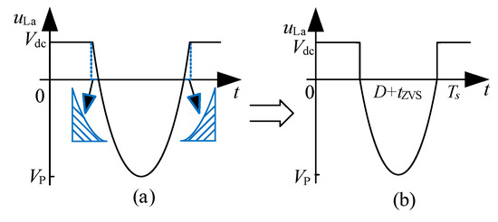
Figure 6.
LCC compensates for the waveform of the network input AC voltage .
According to Figure 6b, the equivalent AC voltage is as follows
According to the volt second balance of the inductance, the inductance voltage is zero in one cycle; the equation is
The peak value of equivalent input voltage can be calculated as
D is the duty ratio, and tzvs is the soft switching margin.
The output impedance RL1, RL2, and RL3 can be expressed as [25]
Due to the good high-order filtering characteristics of the compensation network, the system can be analyzed by using the harmonic approximation method. The equivalent circuit of the system is shown in Figure 7. In order to simplify the analysis process, when the transmitter is far apart, the cross coupling between the transmitter on the same side can be ignored [23]. Theoretically, the number of coils can be expanded to N, and the ripple suppression will be better if the appropriate phase shift angle is found. However, in order to verify the effectiveness of this scheme, three groups of coils are used for theoretical analysis and experimental research.
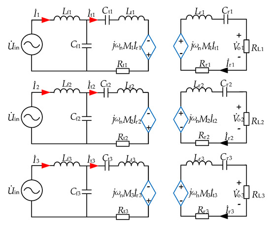
Figure 7.
AC equivalent model of LCC−S.
According to Kirchhoff’s voltage law, the KCL and KVL equations of the LCC−S circuit model in Figure 7 are shown in Equation (5)
According to the operating characteristics of LCC, when the system resonates, the input impedance Zin is pure resistance; when the imaginary part is zero, there is the following relationship [22].
By substituting Equation (6) into (5), the corresponding currents in both sides can be derived as
From Equation (7), the rectifier input voltage of each subsystem is , and .
According to Equation (8), the dc output voltage VL1, VL2, and VL3 can be expressed as
According to Equations (4) and (7), the mutual inductance M1, M2, and M3 between coils is as follows
Therefore, the voltage gains G1, G2, and G3 of each subsystem are as follows
It can be seen from Equation (11) that the voltage gain G is related to the compensation inductance Lf, the mutual inductance M, the equivalent load, and the parasitic resistance of the receiver. Therefore, we can reduce the compensation inductance Lf and increase the voltage gain to reduce the input voltage level.
2.4. Single-Switch LCC-S Circuit Model Parameter Design of Resonance Inductance and Capacitance La and Ca
In order to realize soft switching, according to the design principle of a class E power amplifier, the input resonance frequency fin between the resonance inductance La and the resonance capacitance Ca should be slightly lower than 1.5 times the switching frequency f, as follows [18,19]
The resonance capacitance Ca is selected as
The resonance inductance La is selected as
According to the above parameters, the voltage waveform at both ends of the switch tube is obtained as shown in Figure 8.
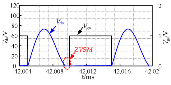
Figure 8.
Soft switching waveforms.
3. System Structure and Phase-Shifting Control
3.1. Ripple Suppression of Input Current
According to Equation (7), the input currents Iin1, Iin2, and Iin3 of each phase subsystem can be expressed as
Fourier decomposition of input current
The , , and can be expressed as
The fundamental waves Iin1, Iin2, and Iin3 and harmonics of the input currents Iin1, Iin2, and Iin3 of each subsystem can be obtained according to Equation (16), and the fundamental waves can be phase-shifted and suppressed according to the vector analysis shown in Equation (18).
If the phase shift angle of subsystem 1 is zero, α and β are the phase shift angles of subsystem 2 and subsystem 3.
According to Equation (17), taking the input voltage of 25 V, the load of 10 Ω, the switching frequency of 100 kHz, and the balanced coupling of three coils as an example, the harmonic content of the input current Iin(t) after Fourier decomposition before and after phase shifting is shown in Figure 9a,b. The black curve in Figure 9a is the input current waveform before phase shifting; it can be decomposed into a DC component, fundamental wave, and superposition of harmonics with Fourier. DC in Figure 9a,b represents the DC component. I–V in Figure 9 represents the DC component fundamental wave and harmonics, respectively. Figure 9a shows that the input current has a large harmonic content and a large fundamental effective value before phase shifting. Figure 9b shows that the input current has a small harmonic content and a small fundamental effective value after phase shifting.
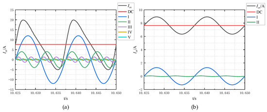
Figure 9.
Input current harmonic content comparison. (a) Harmonic content of input current before phase shift. (b) Input current harmonic content after phase shift.
3.2. System Structure
The system structure diagram is shown in Figure 10. During the transmission process, by adjusting the phase shift conduction angle of the coils α and β, the total current output of the DC source is controlled so that the ripple of the total current is minimized, and the efficiency of the whole machine is higher.
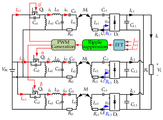
Figure 10.
Schematic diagram of control method.
In the actual system, a single-switch wireless power transfer subsystem is selected as the reference, and its conduction angle is 0°, so the remaining two control degrees of freedom α and β can be obtained according to Equation (18).
4. Verification of Simulation and Experimental Results
4.1. Verification of Simulation Results
The three-coil parallel transmission simulation model was built using MATLAB/Simulink software, and the parameters are shown in Table 2. The switching frequency of the system was 100 kHz, and the duty ratio of the switch tube was set to 0.5.
Table 2.
Prototype parameters of single-switch WPT system.
4.1.1. Verification of Subsystem Balanced Coupling Simulation Results
In order to verify the advantages of P# type single-switch resonant inverter structure, the parameters of traditional and P# type LCC compensation topologies were set to be the same. In the case of the balanced coupling of the system, the input current Iin before and after the phase shift of the traditional single-switch resonant inverter LCC compensation network is shown in Figure 11. When the subsystem adopted the traditional control strategy of simultaneous conduction, the input current was distorted seriously. The THD was 47.1%, the DC component was 7.5 A, and the fundamental wave effective value was 7.7 A. When the subsystem adopted the conduction mode of sequential phase shift of 120°, the current amplitude was greatly reduced, but the current distortion was more serious. The THD was 61.1%. At this time, the DC component was 7.4 A, and the fundamental wave effective value was 1.9 A.
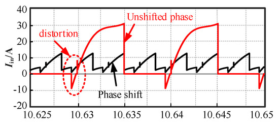
Figure 11.
Comparison of input current before and after phase shifting 120° in traditional single-switch LCC topology.
When the input current Iin of the P# type single-switch resonant inverter LCC compensation network subsystem was simultaneously turned on, as shown in Figure 12, the THD was 32.8%, the DC component was 7.4 A, and the fundamental wave effective value was 11.4 A. The current waveform of the subsystem was smooth after the 120° phase shift in turn. The THD value decreased significantly to only 6.1%, the DC component was 7.4 A, and the fundamental wave effective value decreased to 0.68 A.
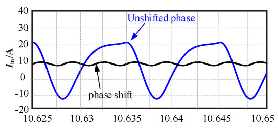
Figure 12.
Comparison of input current before and after phase shift 120° of P# single-switch LCC topology after change.
4.1.2. Verification of Simulation Results of Unbalanced Coupling of Subsystems
In order to verify the universality and effectiveness of the proposed phase shift ripple suppression method, the coupling coefficients of the P# type single-switch resonant inverter subsystem were set to M1 = 50 μH, M2 = 46.4 μH and M3 = 42 μH, respectively. According to Equation (18), the optimal phase shifting angles of the input currents Iin1, Iin2, and Iin3 are 0°, 125.7°, and 239.7°, respectively. The input current Iin is shown in Figure 13. When all subsystems were turned on at the same time, the THD of the input current was 32.9%, the DC component was 7.4 A, and the fundamental effective value was 11.2 A. After the phase shift was turned on, the THD value of the input current decreased greatly to only 9.7%, the DC component was 7.5 A, and the effective value of the fundamental wave was only 0.66 A.
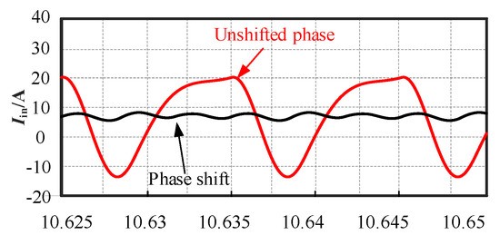
Figure 13.
Comparison of input current before and after phase shift with coupling coefficient M1 = 50 μH, M2 = 46.4 μH, and M3 = 42 μH.
4.2. Verification and Analysis of Experimental Results
In order to further verify the feasibility of the method proposed in this paper, an experimental platform was built, as shown in Figure 14.
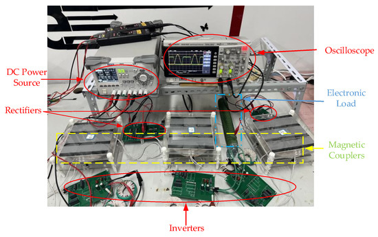
Figure 14.
Experimental prototype.
The main parameters were consistent with the simulation parameters. The controller was STM32F407ZGT6, the drive circuit was UCC27511, and the switch of the P# single-switch resonant inverter was B33N60E power MOSFET. The number of turns of the transmitting and receiving coils was 24 and the diameter was 160 mm. At the same time, a 2 mm thick ferrite was laid on the bottom of the coil to improve the coupling coefficient and shield magnetic leakage. The distance between the transmitter and the receiver was 50 mm.
Figure 15 is a soft switching waveform of the switch tube of the inverter 1. When the driving signal Vgs of the switch changed from the low level at time t1 to the high level at time t2, the drain source voltage Vds of the switch fell to zero, which indicates that the switch realized zero-voltage turn-on.
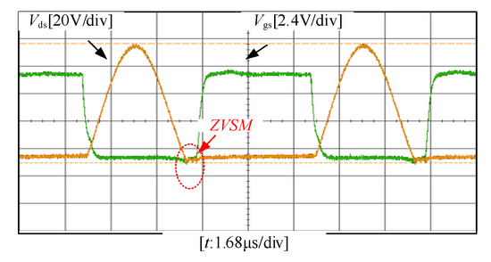
Figure 15.
MOSFET soft switching waveform.
Figure 16 shows waveforms of the input voltage Vo and the input current Ir of the rectifier 1. The RMS of the input voltage Vo was 21.8 V and the RMS of the input current Ir was 2.46 A.
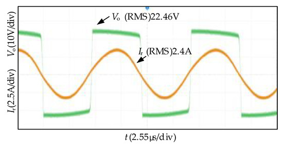
Figure 16.
Rectifier input voltage Vo and current Ir waveform.
Figure 17 is a comparison of the input current Iin of the traditional single-switch resonant inverter and the P# type single-switch resonant inverter LCC compensation topology. Through comparison and analysis, it can be seen that the distortion of the input current Iin of the traditional single-switch resonant inverter was reduced due to the clamping effect of the power supply, but the input current of the P# type LCC compensation topology was smoother.
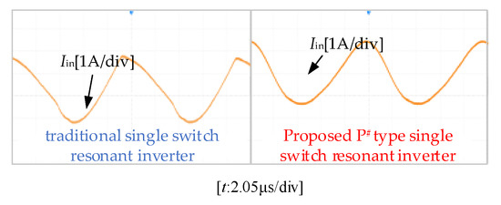
Figure 17.
Comparison of input current Iin waveforms of two compensation topologies.
Figure 18 is a comparison of input current waveforms before and after parallel phase shifting based on the P# type single-switch resonant inverter subsystem under the transmission distance of 50 mm. The input current ripple before phase shifting of the system was large, with a peak-to-peak value of 8.5 A. The input current peak-to-peak value of the subsystem was 2.76 A after phase shifting of 0°, 123.7°, and 241.5°, which greatly reduced the input current ripple and made the input current waveform more stable.
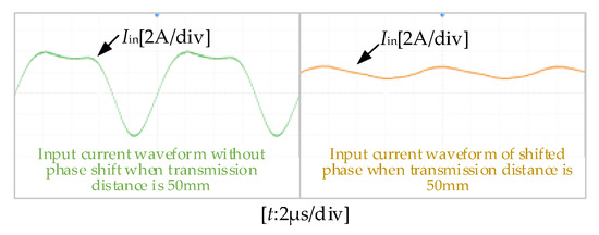
Figure 18.
Input current Iin waveform comparison of shifted phase before and after when the transmission distance is 50 mm.
Figure 19 is the input current waveform before and after parallel phase shifting based on the P# type single-switch resonant inverter subsystem when the transmission distance is 40 mm, 50 mm, and 60 mm, respectively. The peak-to-peak value of the input current before phase shifting of the system was 6.98 A; the peak-to-peak value of the input current of the system was 1.6 A after the subsystem was shifted by 0°, 88.7°, and 251.4°, respectively. It shows that the proposed method also has good anti-offset control performance in the case of asymmetric system parameters.
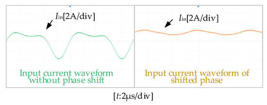
Figure 19.
Input current Iin waveforms comparison of shifted phase before and after when the transmission distance is 40 mm, 50 mm, and 60 mm.
Figure 20 shows the efficiency changes before and after the phase shift of the three coils in parallel by comparing the input voltage of 5–30 V and the load of 5–30 Ω. With the increasing input voltage, when the input voltage was greater than 8 V, the effect after the phase shift was gradually better than that without the phase shift. When the input voltage was 30 V and the load was 15 Ω, the pre-phase-shift efficiency was 84.3% and the post-phase-shift efficiency was 88.2%, an increase of 3.9 percentage points. The fundamental reason is that the proposed control method can effectively improve the input current ripple and improve the system efficiency.
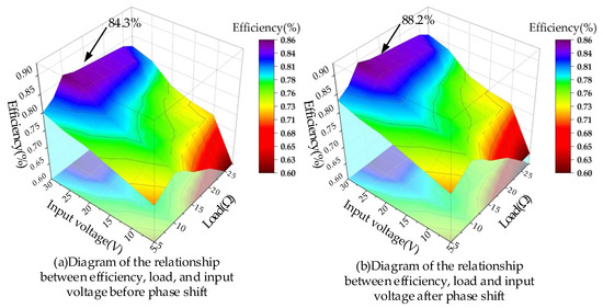
Figure 20.
Comparison of transmission efficiency before and after phase shift.
5. Conclusions
This paper proposes a novel P# type LCC-S compensation network for the single-switch wireless power transfer system of electric-powered vehicles. The proposed method was used to phase shift the ripple to reduce the ripple of the input current and improve the efficiency of the system. Finally, simulation and experimental verification were carried out, which proved the validity and feasibility of this method. The following key conclusions can be drawn:
- (1)
- Connecting the resonant capacitor Ca in parallel with the switch tube can effectively improve the input current waveform and reduce the THD of the input current.
- (2)
- By controlling the phase shift of the excitation current of the multi-coils, the input current ripple can be effectively eliminated, so that the input current becomes stable and the system efficiency can be improved.
- (3)
- When the input voltage was 30 V and the rated power was 150 W, the efficiency of the system increased from 84.3% to 88.2%. It increased by 3.9 percentage points.
Author Contributions
Conceptualization, Y.Y. and X.Z.; formal analysis, S.X., W.Z. and K.G.; investigation, X.Z.; methodology, K.G. All authors have read and agreed to the published version of the manuscript.
Funding
This research was supported by the Youth Project of the National Natural Science Foundation of China (52207004), the Project of Chongqing Banan District of Transformation and industrialization of scientific and technological achievements, grant number 2021TJZ003, and the Graduate Innovation Project of Chongqing University of Technology (gzlcx20223067).
Institutional Review Board Statement
Not applicable.
Informed Consent Statement
Not applicable.
Data Availability Statement
The datasets used and/or analyzed during the current study are available from the corresponding author on request.
Acknowledgments
We want to thank the national active distribution network technology research center of Chongqing University of Technology for the support in the completion of the project.
Conflicts of Interest
The authors declare no conflict of interest.
References
- Yuan, H.; Wang, C. Research on input-parallel single-switch WPT system with load-independent constant voltage output. IEEE Trans. Transp. Electrif. 2023, 9, 1888–1896. [Google Scholar] [CrossRef]
- Li, Y.J.; Hu, F.; Chen, Z. Dual-Phase-Shift control scheme with current-stress and efficiency optimization for wireless power transfer systems. IEEE Trans. Circuits Syst. I Regul. Pap. 2018, 65, 3110–3121. [Google Scholar] [CrossRef]
- Chen, Y.; Zhang, H.; Park, S.-J. A switching hybrid LCC-S compensation topology for constant current/voltage EV wireless charging. IEEE Access 2019, 7, 133924–133935. [Google Scholar] [CrossRef]
- Xie, X.; Xie, C. Constant current output control based on cross-coupling compensation in multireceiver WPT system using active rectifier. IEEE Trans. Transp. Electrif. 2023, 9, 1960–1972. [Google Scholar] [CrossRef]
- Nagashima, T.; Wei, X.; Bou, E. Analysis and design of loosely inductive coupled wireless power transfer system based on class-E2 DC–DC converter for efficiency enhancement. IEEE Trans. Circuits Syst. I Regul. Pap. 2015, 62, 2781–2791. [Google Scholar] [CrossRef]
- Lu, J.; Zhu, G.; Lin, D. Unified Load-Independent ZPA analysis and design in cc and cv modes of higher order resonant circuits for WPT Systems. IEEE Trans. Transport. Electrif. 2019, 5, 977–987. [Google Scholar] [CrossRef]
- Yao, Y.; Wang, Y.; Liu, X. Analysis and Design of an S/SP Compensated IPT System to Minimize Output Voltage Fluctuation Versus Coupling Coefficient and Load Variation. IEEE Trans. Veh. Technol. 2018, 67, 9262–9272. [Google Scholar] [CrossRef]
- Cota, K.A.; Gray, P.A.; Lehn, P.W. An Approach for Selecting Compensation Capacitances in Resonance-Based EV Wireless Power Transfer Systems with Switched Capacitors. IEEE Trans. Transport. Electrific. 2019, 5, 1004–1014. [Google Scholar] [CrossRef]
- Li, S.; Li, W.; Deng, J. Double-sided LCC compensation network and its tuning method for wireless power transfer. IEEE Trans. Veh. Technol. 2015, 64, 2261–2273. [Google Scholar] [CrossRef]
- Budhia, M.; Boys, J.T.; Covic, G.A. Development of a single-sided flux magnetic coupler for electric vehicle IPT charging systems. IEEE Trans. Ind. Electron. 2013, 60, 318–328. [Google Scholar] [CrossRef]
- Zhao, B.; Yu, Q.; Sun, W. Extended-phase-shift control of isolated bidirectional DC–DC converter for power distribution in microgrid. IEEE Trans. Power Electron. 2012, 27, 4667–4680. [Google Scholar] [CrossRef]
- Lin, F.Y.; Kim, S.; Covic, G.A. Effective coupling factors for series and parallel tuned secondaries in IPT systems using bipolar primary pads. IEEE Trans. Transp. Electrific. 2017, 3, 434–444. [Google Scholar] [CrossRef]
- Zaheer, A.; Hao, H.; Covic, G.A. Investigation of multiple decoupled coil primary pad topologies in lumped IPT systems for interoperable electric vehicle charging. IEEE Trans. Power Electron. 2015, 30, 1937–1955. [Google Scholar] [CrossRef]
- Li, H.; Fang, J.; Chen, S. Pulse density modulation for maximum efficiency point tracking of wireless power transfer systems. IEEE Trans. Power Electron. 2018, 33, 5492–5501. [Google Scholar] [CrossRef]
- Bac, N.X.; Vilathgamuwa, D.M.; Madawala, U.K. A SiC-based matrix converter topology for inductive power transfer system. IEEE Trans. Power Electron. 2014, 29, 4029–4038. [Google Scholar]
- Zahid, Z.U. Modeling and control of series–series compensated inductive power transfer system. IEEE J. Emerg. Sel. Topics Power Electron. 2015, 3, 111–123. [Google Scholar] [CrossRef]
- Chen, Y.; Kou, Z.; Zhang, Y. Hybrid topology with configure rable charge current and charge voltage output based WPT charger for massive electric bicycles. IEEE J. Emerg. Sel. Top. Power Electron. 2018, 6, 1581–1594. [Google Scholar] [CrossRef]
- Roslaniec, L.; Jurkov, A.S.; Bastami, A.A. Design of Single-Switch Inverters for Variable Resistance/Load Modulation Operation. IEEE Trans. Power Electron. 2015, 30, 3200–3214. [Google Scholar] [CrossRef]
- Li, Y.; Hu, J.; Chen, F. A new-variable-coil-structure-based IPT system with load-independent constant output current or voltage for charging electric bicycles. IEEE Trans. Power Electron. 2018, 33, 8226–8230. [Google Scholar] [CrossRef]
- Qu, X.; Chu, H.; Wong, S. An IPT battery charger with near unity power factor and load-independent constant output combating design constraints of input voltage and transformer parameters. IEEE Trans. Power Electron. 2019, 34, 7719–7727. [Google Scholar] [CrossRef]
- Dai, X.; Jiang, J.; Wu, J. Charging area determining and power enhancement method for multi-excitation unit configuration of wirelessly dynamic charging EV System. IEEE Trans. Ind. Electron. 2019, 66, 4086–4096. [Google Scholar] [CrossRef]
- Zhu, A.; Zhou, H.; Deng, Q.; Shao, Y.; Chen, J.; Hu, W.; Li, S. Modeling and phase synchronization control of high-power wireless power transfer system supplied by modular parallel multi-inverters. IEEE Trans. Veh. Technol. 2021, 70, 6450–6462. [Google Scholar] [CrossRef]
- Li, Y.; Hu, J.; Li, X.; Mai, R.; Li, Z.; Liu, M.; He, Z. Efficiency analysis and optimization control for input-parallel output-series wireless power transfer systems. IEEE Trans. Power Electron. 2020, 35, 1074–1085. [Google Scholar] [CrossRef]
- Huang, Y.; Lee, A.T.L.; Tan, S.-C. Highly efficient wireless power transfer system with single-switch step-up resonant inverter. IEEE J. Emerg. Sel. Top. Power Electron. 2021, 9, 1157–1168. [Google Scholar] [CrossRef]
- Houji, L.; Chunfang, W.; Rui, Y. Research on single-switch wireless power transfer circuit based on SiC device. Proc. CSEE 2020, 40, 1808–1817. [Google Scholar]
- Zhang, K.; Ma, Y.; Yan, Z. Current loss and detuning effect of seawater on wireless power transfer. IEEE J. Emerg. Sel. Topics Power Electron. 2020, 8, 909–917. [Google Scholar] [CrossRef]


Disclaimer/Publisher’s Note: The statements, opinions and data contained in all publications are solely those of the individual author(s) and contributor(s) and not of MDPI and/or the editor(s). MDPI and/or the editor(s) disclaim responsibility for any injury to people or property resulting from any ideas, methods, instructions or products referred to in the content. |
© 2023 by the authors. Licensee MDPI, Basel, Switzerland. This article is an open access article distributed under the terms and conditions of the Creative Commons Attribution (CC BY) license (https://creativecommons.org/licenses/by/4.0/).