
A Compact Hybrid G-band Heterodyne Receiver Integrated with Millimeter Microwave Integrated Circuits and Schottky Diode-Based Circuits

 ,
,
Abstract
:1. Introduction
2. Configuration and Design
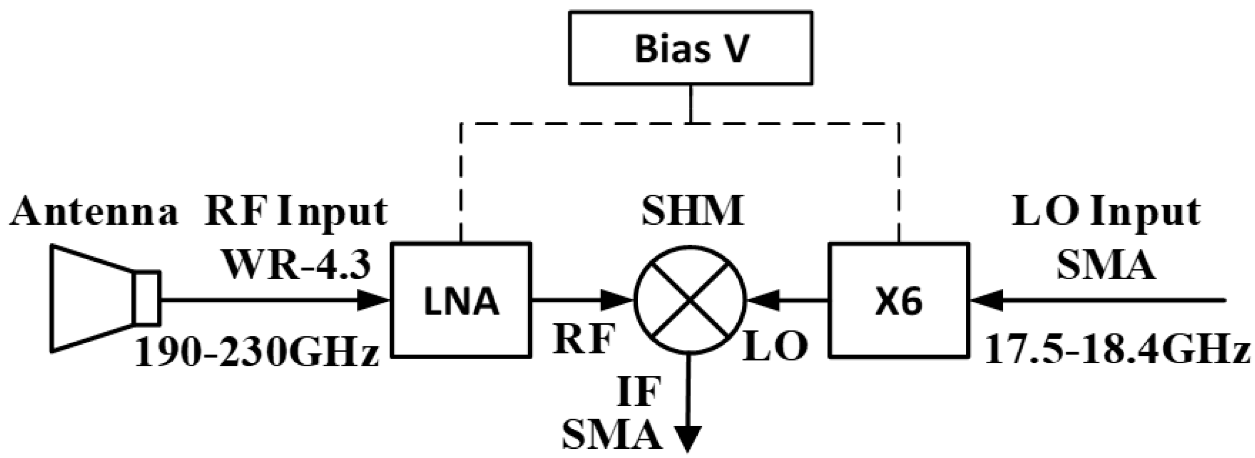
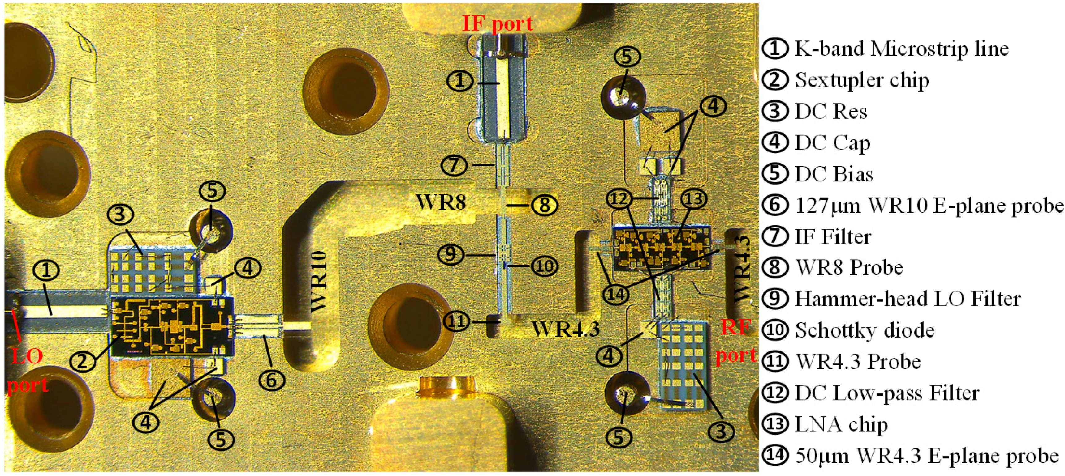
2.1. Overview
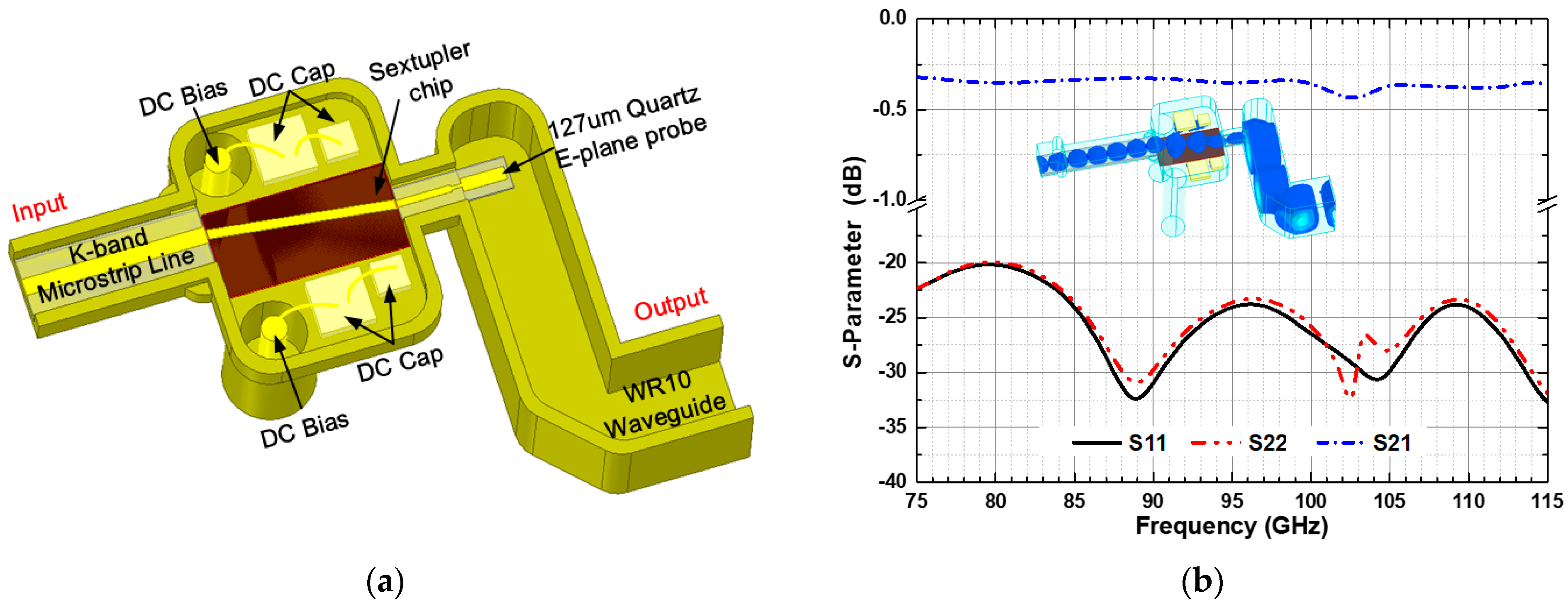
2.2. LO Sextupler Design
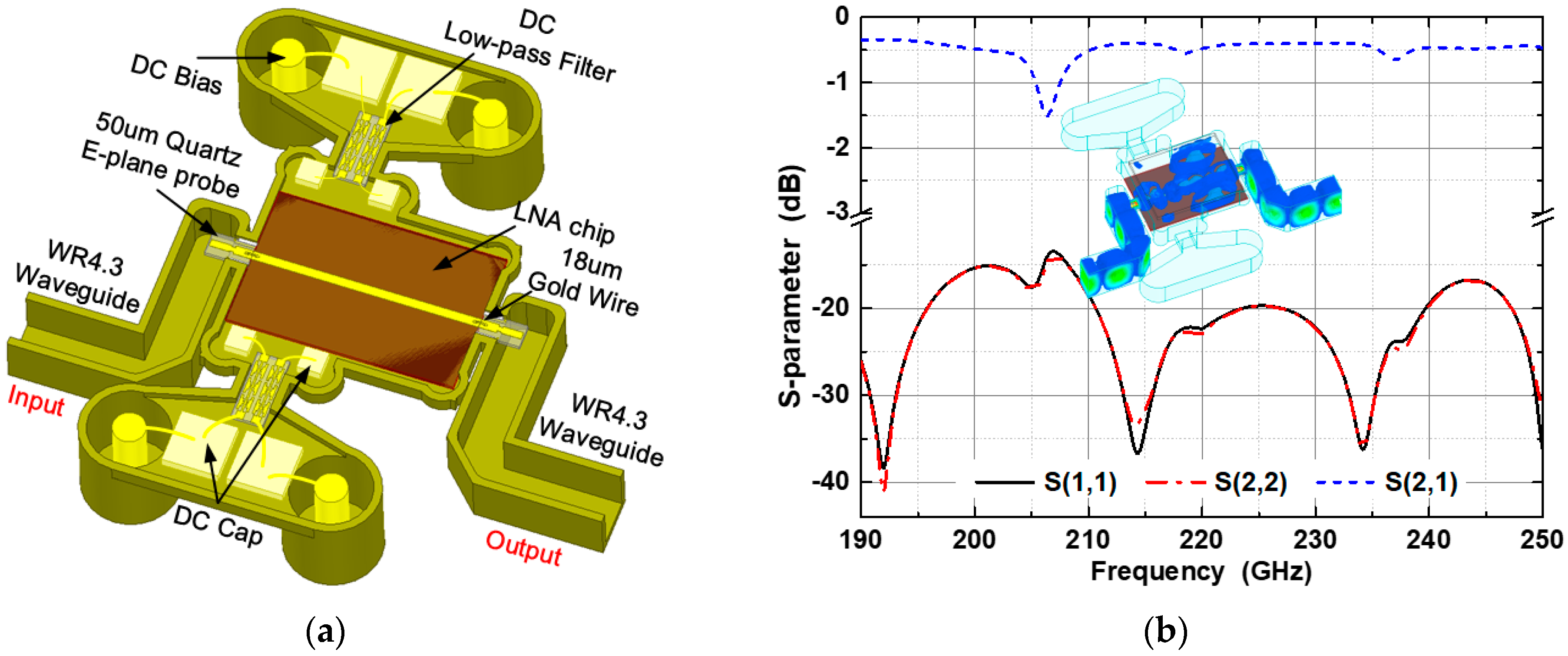
2.3. RF Low-Noise Amplifier Design
2.4. Sub-Harmonic Mixer Design
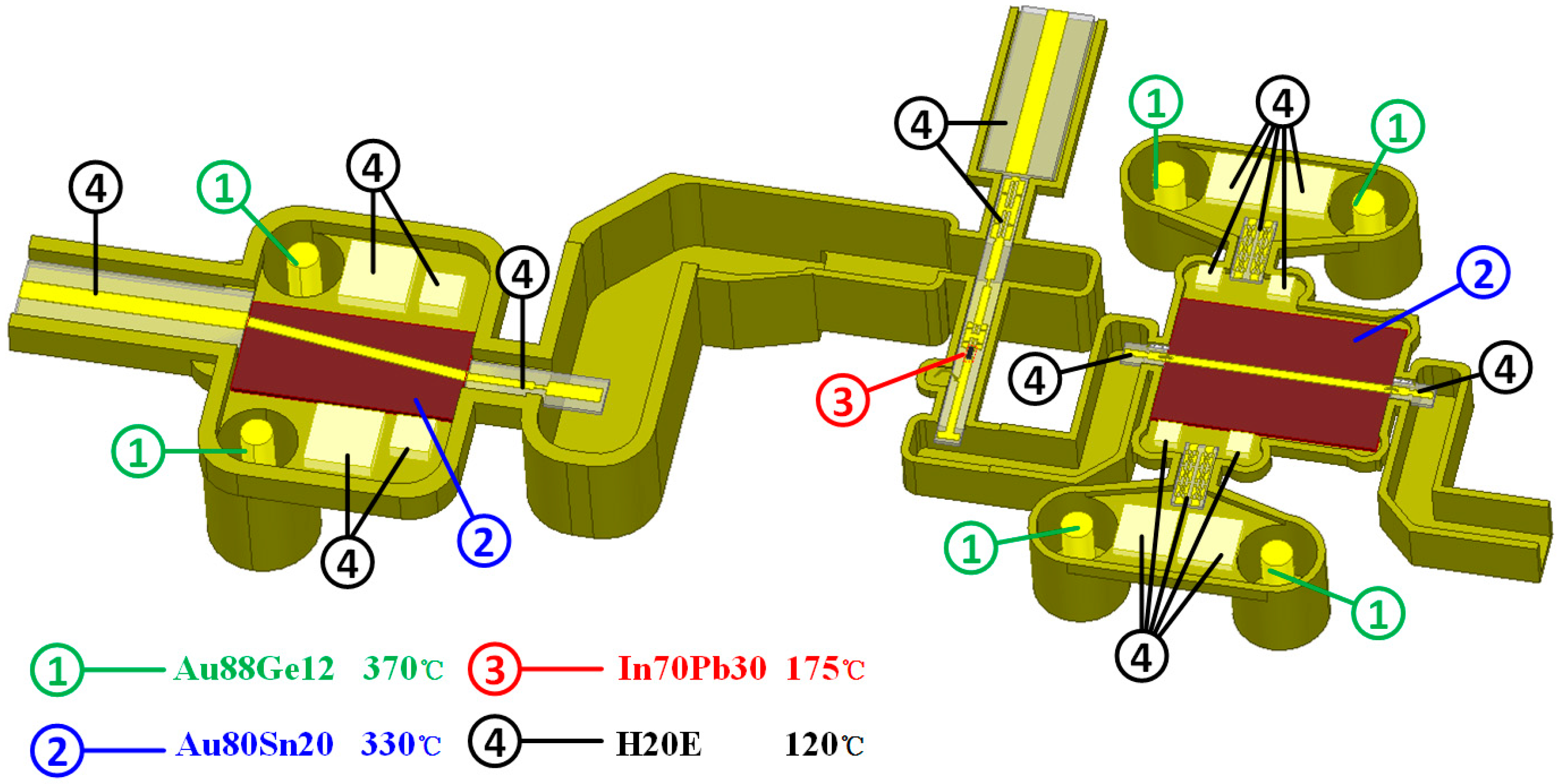
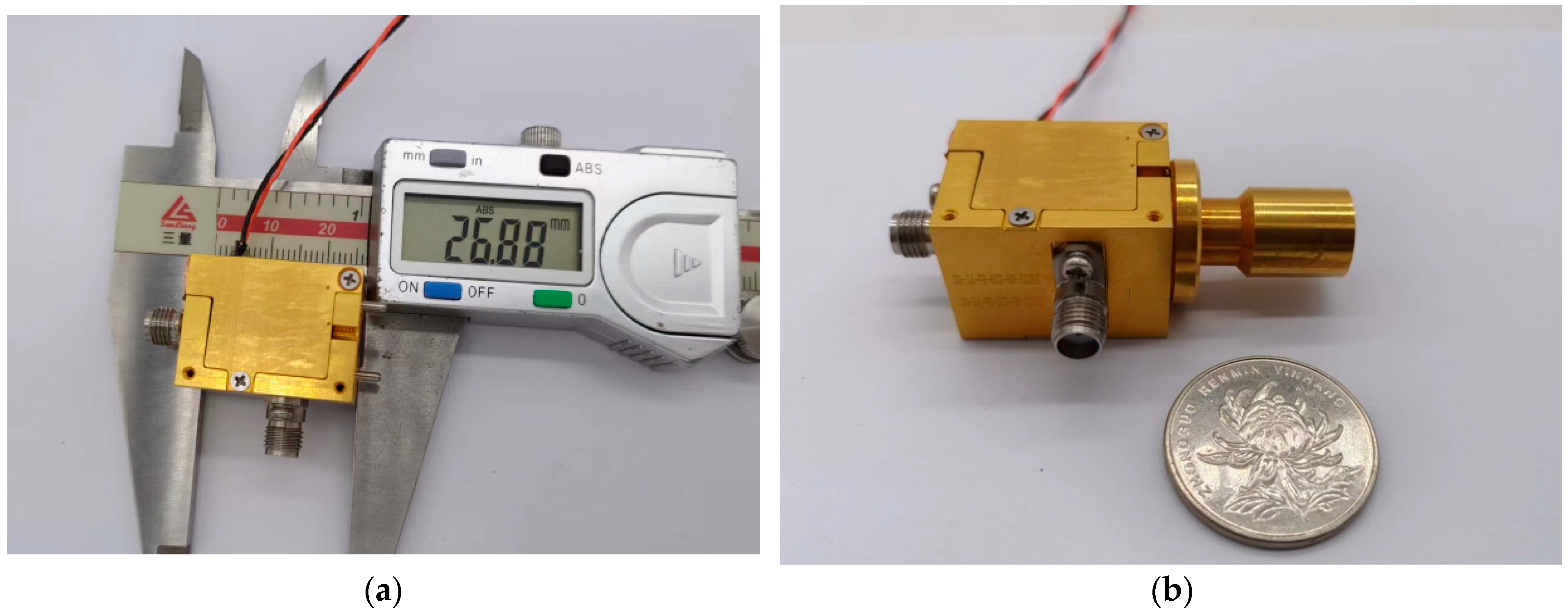
3. Module Assembly
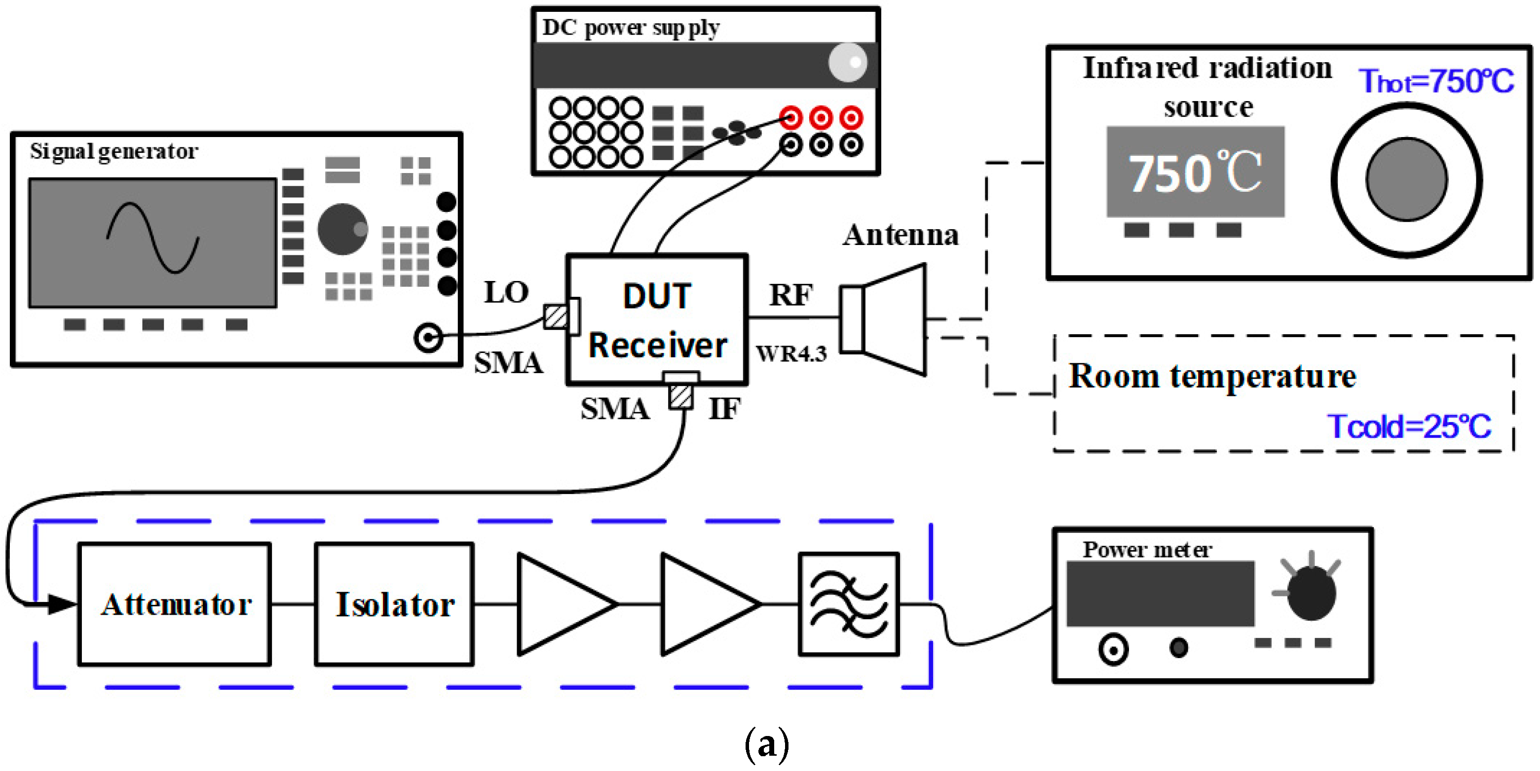
4. Measurement Results
4.1. Conversion Gain
4.2. DSB Noise Temperature
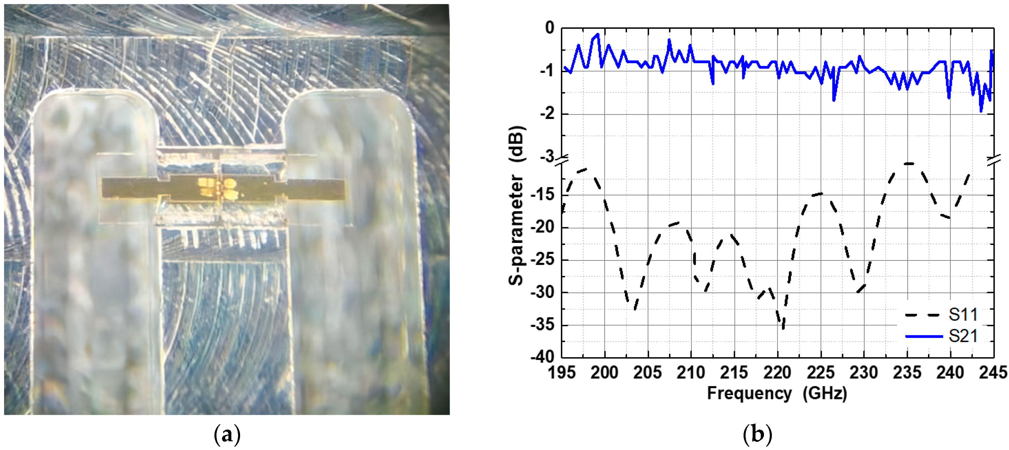
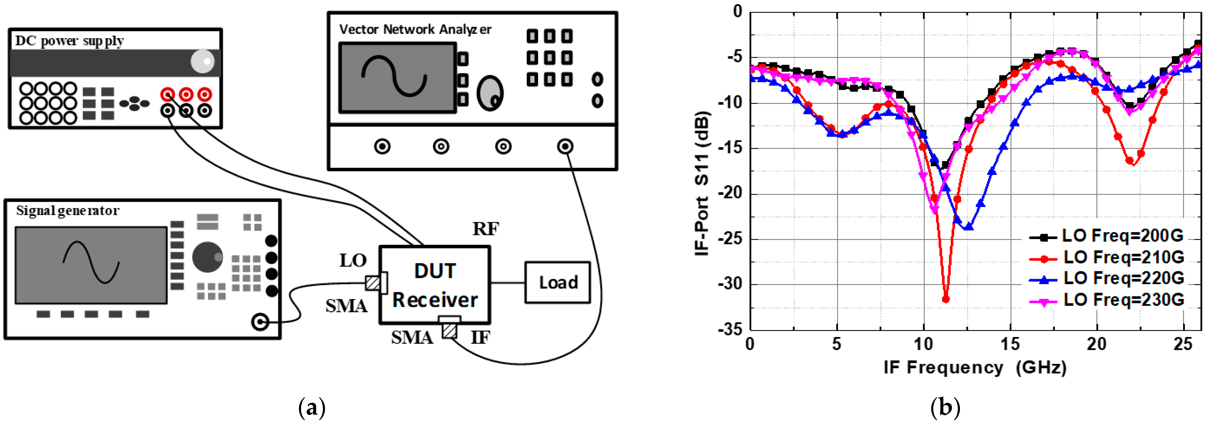
4.3. S-Parameters
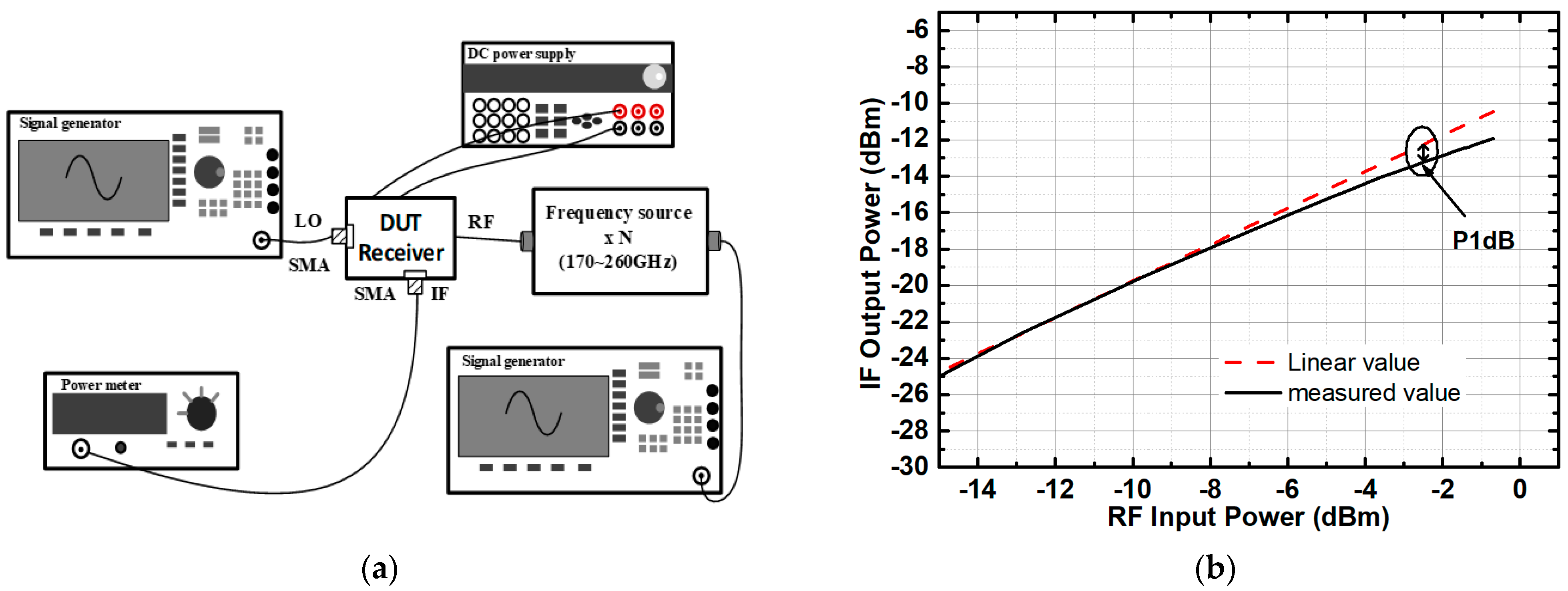
4.4. P1dB
4.5. IF Spectrum
5. Conclusions
Author Contributions
Funding
Conflicts of Interest
References
- White Paper on RF Enabling 6G—Opportunities and Challenges from Technology to Spectrum. Available online: https://www.6gflagship.com/white-paper-on-rf-enabling-6g-opportunities-and-challenges-from-technology-to-spectrum (accessed on 12 April 2021).
- Wang, C.X.; You, X.; Gao, X.; Zhu, X.; Li, Z.; Zhang, C.; Wang, H.; Huang, Y.; Chen, Y.; Haas, H. On the Road to 6G: Visions, Requirements, Key Technologies and Testbeds. IEEE Commun. Surv. Tuts. 2023, 25, 905–974. [Google Scholar] [CrossRef]
- Lin, C.; Li, G.Y. Terahertz communications: An array-of-subarrays solution. IEEE Commun. Mag. 2016, 54, 124–131. [Google Scholar] [CrossRef]
- Han, C.; Akyildiz, I.F. Distance-Aware Bandwidth-Adaptive Resource Allocation for Wireless Systems in the Terahertz Band. IEEE Trans. Terahertz Sci. Technol. 2016, 6, 541–553. [Google Scholar] [CrossRef]
- Wu, Y.; Lemic, F.; Han, C.; Chen, Z. Sensing Integrated DFT-Spread OFDM Waveform and Deep Learning-powered Receiver Design for Terahertz Integrated Sensing and Communication Systems. IEEE Trans. Commun. 2023, 71, 595–610. [Google Scholar] [CrossRef]
- Akyildiz, I.F.; Jornet, J.M.; Han, C. Terahertz band: Next frontier for wireless communications. Phys. Commun. 2014, 12, 16–32. [Google Scholar] [CrossRef]
- Cheng, B.; Cui, Z.; Lu, B.; Qin, Y.; Liu, Q.; Chen, P.; He, Y.; Jiang, J.; He, X.; Deng, X.; et al. 340-GHz 3-D Imaging Radar With 4Tx-16Rx MIMO Array. IEEE Trans. Terahertz Sci. Technol. 2018, 8, 509–519. [Google Scholar] [CrossRef]
- Cui, Z.M.; Gao, J.K.; Lu, B. Real time 3D imaging system based on sparse MIMO array at 340 GHz. J. Infr. Millim. Waves 2017, 36, 102–106. [Google Scholar]
- Kotiranta, M.; Jacob, K.; Kim, H.; Hartogh, P.; Murk, A. Optical Design and Analysis of the Submillimeter Wave Instrument on JUICE. IEEE Trans. Terahertz Sci. Technol. 2018, 8, 588–595. [Google Scholar] [CrossRef]
- Thomas, B.; Brandt, M.; Walber, A.; Gibson, H.; Philipp, M.; Sonnabend, G.; Benzazaa, M.; Gonzalez, R.; Bergada, M.; Martinez, J.; et al. Millimeter & submillimeter wave radiometer instruments for the next generation of polar orbiting meteorological satellites—MetOp-SG. In Proceedings of the 2014 39th International Conference on Infrared, Millimeter, and Terahertz Waves (IRMMW-THz), Tucson, AZ, USA, 14–19 September 2014; pp. 1–3. [Google Scholar]
- Rappaport, T.S.; Xing, Y.; Kanhere, O.; Ju, S.; Madanayake, A.; Mandal, S.; Alkhateeb, A.; Trichopoulos, G.C. Wireless communications and applications above 100 GHz: Opportunities and challenges for 6G and beyond. IEEE Access 2019, 7, 78729–78757. [Google Scholar] [CrossRef]
- Li, O.; He, J.; Zeng, K.; Yu, Z.; Du, X.; Zhou, Z.; Liang, Y.; Wang, G.; Chen, Y.; Zhu, P.; et al. Integrated sensing and communication in 6G: A prototype of high resolution multichannel THz sensing on portable device. EURASIP J. Wirel. Commun. Netw. 2022, 2022, 106–127. [Google Scholar] [CrossRef]
- Wang, C.; Lu, B.; Lin, C.; Chen, Q.; Miao, L.; Deng, X.; Zhang, J. 0.34 THz Wireless Link Based on High Order Modulation for Future Wireless Local Area Network. IEEE Trans. Terahertz Sci. Technol. 2014, 4, 7–85. [Google Scholar] [CrossRef]
- Wang, C.; Lin, C.; Chen, Q.; Lu, B.; Deng, X.; Zhang, J. A 10 Gbit/s Wireless Communication Link Using 16QAM Modulation in 140 GHz Band. IEEE Trans. Microw. Theory Technol. 2013, 61, 2737–2746. [Google Scholar] [CrossRef]
- Chen, Z.; Chen, X.; Cui, W.; Li, X.; Ge, J. A High-Power G-band Schottky Local Oscillator Chain for Submillimeter Wave Heterodyne Detection. J. Infrared Milli. Terahz. Waves 2015, 36, 430–444. [Google Scholar] [CrossRef]
- Chen, Z.; Chen, X.; Cui, W.; Li, X.; Ge, J. A G-Band 2-Pixel Heterodyne Receiver with Integrated Local Oscillator Chain. J. Infrared Milli. Terahz. Waves 2019, 40, 1035–1051. [Google Scholar] [CrossRef]
- Yao, C.; Chen, Z.; Ge, J.; Zhou, M.; Wei, X. A compact 220 GHz heterodyne receiver module with planar Schottky diodes. Int. J. Electron. Commun. 2018, 84, 153–161. [Google Scholar] [CrossRef]
- Yang, Y.; Zhang, B.; Zhao, X.; Fan, Y.; Chen, X. 220 GHz wideband integrated receiver front end based on planar Schottky diodes. Microw. Opt. Technol. Lett. 2020, 62, 2737–2746. [Google Scholar] [CrossRef]
- Li, Y.; Zhang, Y.; Wu, C.; Cui, J.; Zhu, H.; Yan, B. A 16-QAM 45-Gbps 7-m wireless link using InP HEMT LNA and GaAs SBD mixers at 220-GHz-band. China Commun. 2021, 18, 255–262. [Google Scholar] [CrossRef]
- Abbasi, M.; Gunnarsson, S.E.; Wadefalk, N.; Kozhuharov, R.; Svedin, J.; Cherednichenko, S.; Angelov, I.; Kallfass, I.; Leuther, A.; Zirath, H. Single-chip 220-GHz active heterodyne receiver and transmitter MMICs with on-chip integrated antenna. IEEE Trans. Microw. Theory Tech. 2010, 59, 466–478. [Google Scholar] [CrossRef]


| Reference | Frequency (GHz) | Conversion Gain (dB) | Noise Temperature (K) | Dimensions (mm × mm × mm) | Configuration |
|---|---|---|---|---|---|
| [10] | 173–205 | −20~−13 | Not indicated | ≈80 × 30 × 40 | Discrete |
| [11] | 209.4–219.6 | −8.4~−6.2 | 725~1550 | 150 × 60 × 19.1 | Discrete |
| [12] | 185–250 | −11~−7.5 | 750–1600 | 20 × 20 × 35 | Integrated front-end |
| [13] | 221–236 | +9.3 | 3052.8 | 80 × 40 × 20 | Discrete |
| This work | 195–230 | +10.5~+17.5 | 1009–1158 | 27 × 20 × 20 | Integrated front-end + LNA |
Disclaimer/Publisher’s Note: The statements, opinions and data contained in all publications are solely those of the individual author(s) and contributor(s) and not of MDPI and/or the editor(s). MDPI and/or the editor(s) disclaim responsibility for any injury to people or property resulting from any ideas, methods, instructions or products referred to in the content. |
© 2023 by the authors. Licensee MDPI, Basel, Switzerland. This article is an open access article distributed under the terms and conditions of the Creative Commons Attribution (CC BY) license (https://creativecommons.org/licenses/by/4.0/).
Share and Cite
Huang, K.; Zhang, L.; Li, R.; Tian, Y.; He, Y.; Jiang, J.; Deng, X.; Su, W. A Compact Hybrid G-band Heterodyne Receiver Integrated with Millimeter Microwave Integrated Circuits and Schottky Diode-Based Circuits. Electronics 2023, 12, 2806. https://doi.org/10.3390/electronics12132806
Huang K, Zhang L, Li R, Tian Y, He Y, Jiang J, Deng X, Su W. A Compact Hybrid G-band Heterodyne Receiver Integrated with Millimeter Microwave Integrated Circuits and Schottky Diode-Based Circuits. Electronics. 2023; 12(13):2806. https://doi.org/10.3390/electronics12132806
Chicago/Turabian StyleHuang, Kun, Liang Zhang, Ruoxue Li, Yaoling Tian, Yue He, Jun Jiang, Xianjin Deng, and Wei Su. 2023. "A Compact Hybrid G-band Heterodyne Receiver Integrated with Millimeter Microwave Integrated Circuits and Schottky Diode-Based Circuits" Electronics 12, no. 13: 2806. https://doi.org/10.3390/electronics12132806
APA StyleHuang, K., Zhang, L., Li, R., Tian, Y., He, Y., Jiang, J., Deng, X., & Su, W. (2023). A Compact Hybrid G-band Heterodyne Receiver Integrated with Millimeter Microwave Integrated Circuits and Schottky Diode-Based Circuits. Electronics, 12(13), 2806. https://doi.org/10.3390/electronics12132806