1. Introduction
In recent years, the exhaustion of spectrum resources in the microwave band has motivated the adoption of a higher and wider spectrum [
1]. Following this trend of enhancing the carrier frequencies, the Terahertz (THz) (0.1–10 THz) band is envisioned as one of the key technologies for supporting the sixth generation (6G) of wireless communication systems [
2]. The THz band’s extraordinarily wide bandwidth provides extremely high sensing precision, as well as extremely fast transmission speeds of up to hundreds of Gbps, and potentially Tbps [
3,
4]. THz waves have a short wavelength; hence tiny antennas are expected to be used to enable highly portable and wearable electronics [
5]. Additionally, the non-ionization of THz radiation guarantees the safety of THz devices for the human body [
6].
Over the past years, heterodyne transceivers have always been preferred in numerous terahertz applications, including security imaging, earth observation, and high data-rate communications [
7,
8,
9,
10,
11]. Researchers in the field of Integration of Sensing and Communication (ISAC) are increasingly fascinated with the terahertz band because of its unique advantages, including small device size, ultra-high data rate up to Tbit/s, strong sensing ability, and high security at the physical layer [
12]. Traditional terahertz transceivers, which still consist of a number of discrete modules in cascade and operate well, fall short when highly integrated and compact systems are required. To perform the up/down-convert function, traditional terahertz transceivers often require numerous independent functional modules in a cascade [
13,
14,
15,
16,
17,
18,
19]. However, the latest generation of terahertz front ends, applied in spaceborne and airborne platforms, put forward the requirements of miniaturization. As a consequence, the development of highly integrated terahertz Radio Frequency (RF) front-end modules with competitive performance is quite worthwhile.
Using a single integrated multi-function receiver chip to develop compact receivers is indeed a highly integrated, low-cost mainstream approach. However, this paper focuses on a method that incorporates both packaged Schottky diodes and MMICs. This method has several advantages over the multifunctional integrated receiver chip in reference [
20], as follows: (1) High design flexibility. Modules with varying frequency bands and functionalities can be rapidly developed to accommodate diverse system requirements. (2) Better performance. Owing to the inherent properties of the components, Schottky diodes exhibit certain advantages over chips in terms of key metrics for a mixer, such as conversion loss and noise figure. (3) Shorter research and iteration cycles. The design and development process for discrete components exhibits a shorter iteration cycle compared to that of integrated chip design. (4) Enhanced modularity. The system architecture permits the integration of additional components, such as filters and power dividers, to accommodate specialized system requirements. Therefore, this study presents a viable alternative for compact packaging of terahertz receivers with superior performance.
In this paper, a hybrid method of assembly is used to combine MMICs and a Schottky diode-based circuit in a single container. With this method, a single module performs the functions of a low-noise amplifier, harmonic mixer, and local oscillator drive. Due to their different degrees of heat tolerance, Schottky diodes and MMICs require solders with various melting points during the micro-assembly process. Before each component is baked and welded, the solders must be organized according to the melting point, beginning with the greatest melting point and moving down. Finally, by merging electromagnetic and thermal co-simulation design, a miniaturized full-function terahertz receiver is made possible. Its efficacy might be superior to that of a standard terahertz receiver with cascaded discrete functional modules.
The rest of this article is structured as follows. We describe each module in the hypothetical G-band receiver in
Section 2. Then, in
Section 3, the receiver’s overall assembly information is presented, and in
Section 4, the receiver’s measurement results are provided. Finally, in
Section 5, we reach our conclusions.
2. Configuration and Design
2.1. Overview
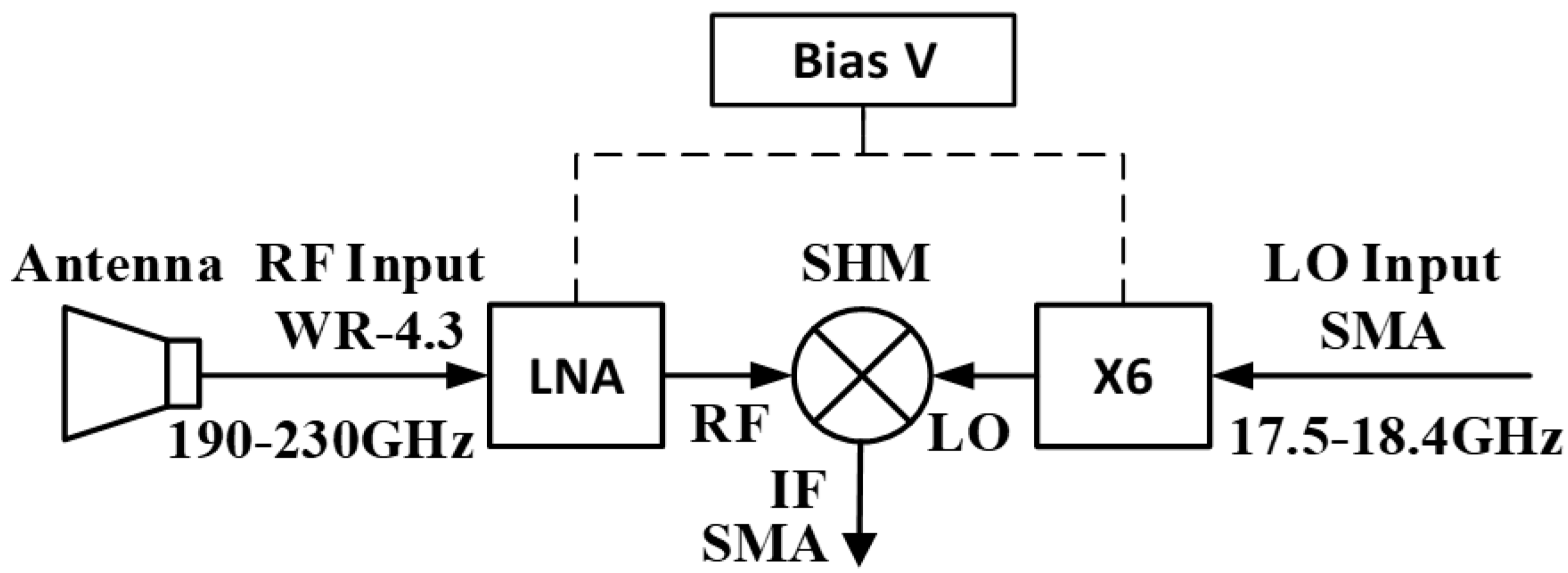
Figure 1 depicts the schematic layout of a terahertz receiver. The W-band (75–110 GHz) sextupler chip, the Schottky diode-based Sub-Harmonic Mixer (SHM), and the terahertz Low Noise Amplifier (LNA) chip make up the majority of the terahertz receiver. Through a coaxial connector, the Local Oscillator (LO) signal enters the module. The 17.5–18.4 GHz signal is then multiplied by a sextupler chip to produce the W-band, which is used for providing the LO signal to the SHM. Additionally, the antenna receives the G-band RF signal, which is then channeled through the WR-4.3 rectangle waveguide and into the module. The SHM then downconverts the RF signal amplified by the LNA chip to Intermediate Frequency (IF).
2.2. LO Sextupler Design
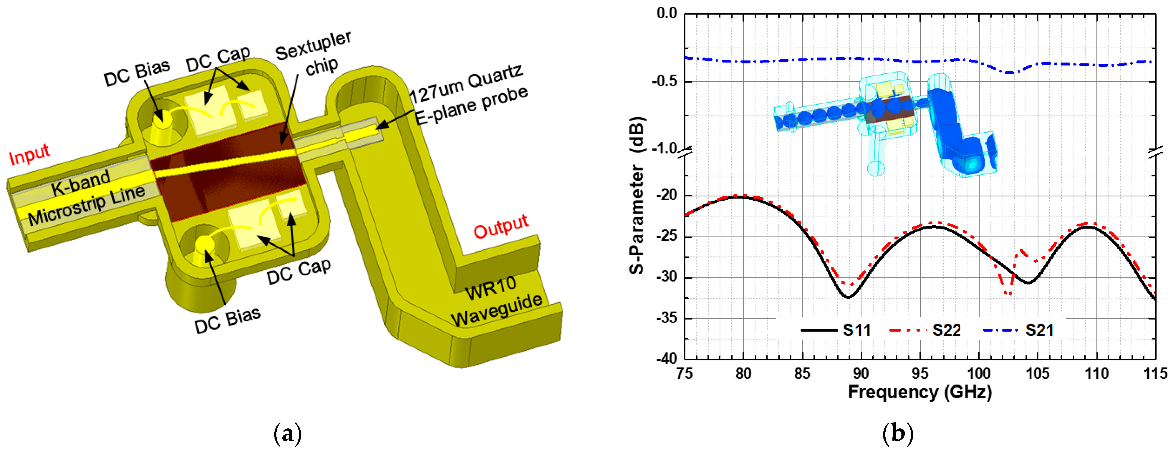
An active sextupler is used to deliver adequate LO power to the mixer in order to convert the input K-band signals to W-band. This component uses an active sextupler chip, which can multiply signals from the 17.5 GHz to 18.4 GHz band to the 105 GHz to 110 GHz band. The output power of the sextupler chip is approximately 6 dBm when pumped with 16 dBm of input power. The InP High Electron Mobility Transistor (HEMT) process is utilized for manufacturing the sextupler chip. For the adjacent harmonics (fifth and seventh harmonics) suppression, the chip is a sextupler chip with a typical value of 20 dBc. In normal circumstances, a common supply voltage of +4 V is used for all the drains, and −0.35 V of the gate voltage is provided to bias the chip depending on its operating condition. The drain current is 80 mA for the chip. The chip was 1.33 mm in width, 70 μm in thickness, and 2.8 mm in length (input and output directions).
Firstly, as seen in
Figure 2a, it is decided that the E-plane probe would transmit the 75–110 GHz output signal into the WR-10 rectangle waveguide, which is fabricated with a 127 μm-thick quartz substrate. Then, the probe and the chip packaging cavity need to be evaluated as a whole.
Figure 2b shows that the W-band E-plane probe’s simulated S-parameters result in a full-band return loss that is better than 20 dB.
2.3. RF Low-Noise Amplifier Design
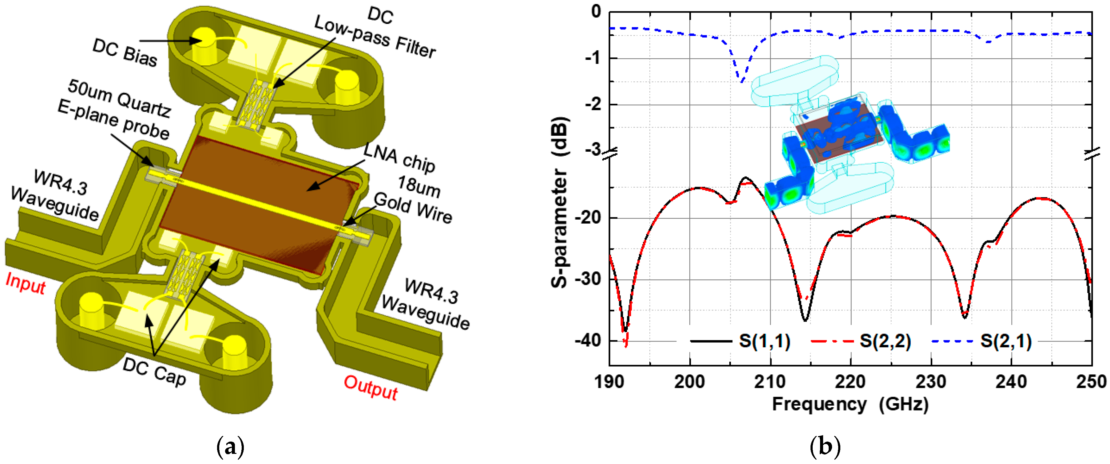
The low-noise amplifier chip is also manufactured by the InP HEMT process. The datasheet of the chip shows that this chip has a linear gain of better than 24 dB and a typical noise figure of 5.8 dB on the chip tested in the 195 GHz and 230 GHz operating bands. The drain current is 37 mA on typical conditions, which requires a common supply voltage of +1.2 V for all of the drains and −0.3 V of the gate voltage to bias the chip depending on its operating conditions. The chip was 0.97 mm in width, 50 μm in thickness, and 2.14 mm in length (input and output directions).
Figure 3a illustrates the factors that must be taken into consideration during the 3D EM simulation of the G-band low-noise amplifier module. Microstrip probes are suspended in the G-band E-plane and attached to the chip’s input and output ports. The DC supply cavities on both sides are divided and connected using just an over-DC low-pass filter in order to prevent resonance of the chip’s RF cavity. The microscale impacts of the electromagnetic field are particularly sensitive to the G-band, where the low-noise amplifier operates. As a result, when designing the THz low-loss waveguide transition probe, it is essential to model and simulate the arc and arc duration of the bonding wire. According to
Figure 3b, the simulated transmission line and both sides of the transition probes with 18 um bonded gold wire have a total transmission loss of 0.5 dB at the 210–230 GHz band. As a rule of thumb, during wire bonding, the gold wire should be as flattened as feasible because the loss of a gold wire will rise with its length and height.
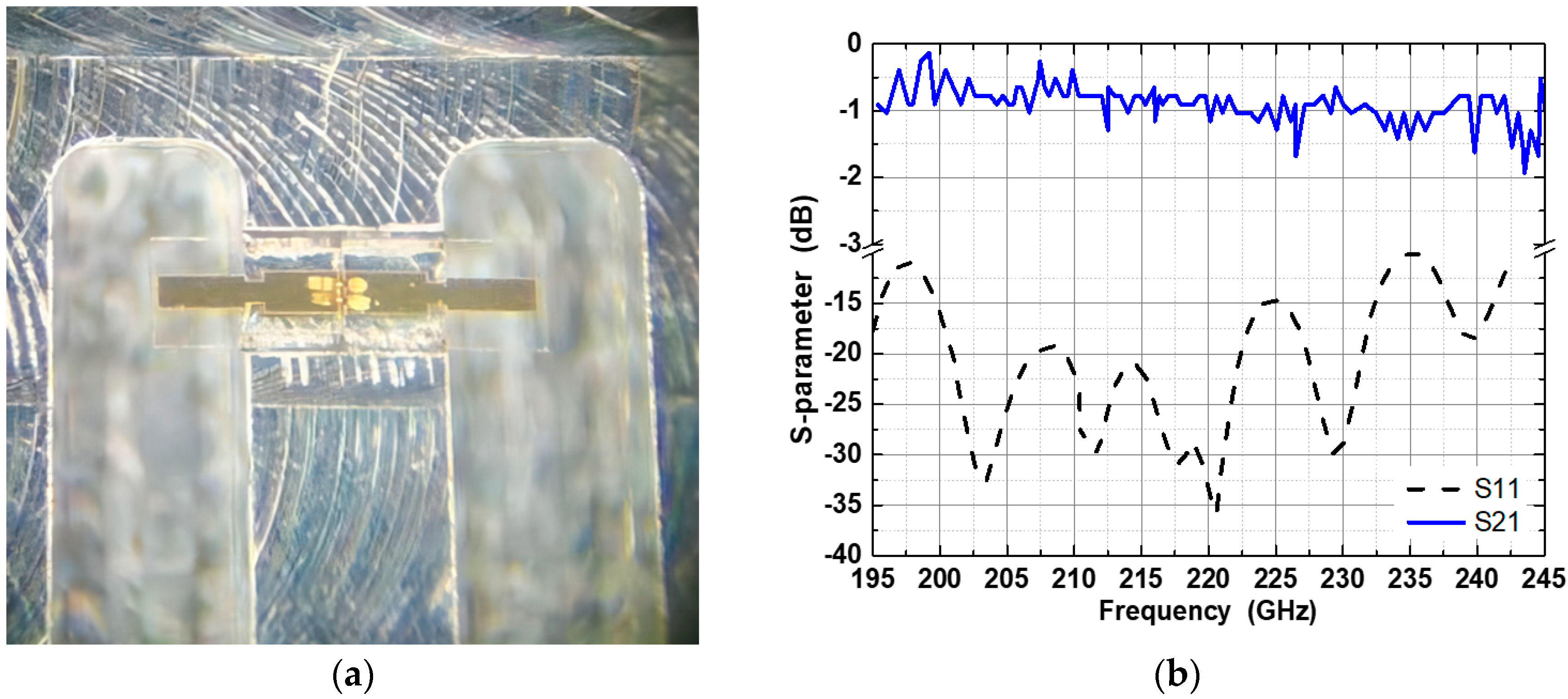
In order to test various probes for rectangular waveguide transition structures, specialized fixtures were created, as seen in
Figure 4a. The probes are positioned back-to-back in the fixture and connected using gold wire bonding. Additionally, it has been determined through comparison trials of several probe types that the suspended microstrip probe performs best in the G-band.
Figure 4b displays the probe’s back-to-back S-parameter performance. The demonstrated back-to-back probe exhibits a typical transmission loss of 1 dB in the 200 GHz to 230 GHz frequency range, from which the loss of a single-ended E-probe could be derived by multiplying a factor of 0.5.
2.4. Sub-Harmonic Mixer Design
The G-band SHM’s construction is shown in
Figure 5a. The G-band SHM’s RF signal is supplied into the mixer Schottky diode pair through the WR4.3 rectangle waveguide, and then out to the microstrip probe. On the opposite side of the Schottky diode pair, the WR-8 rectangular waveguide supplies the LO signal. To decrease the RF signal leakage to the LO port, and stop the RF signal and LO signal from interfering with each other, a low pass filter must be installed at the end of the LO signal, near the Schottky diode. This will ensure that the input of the LO signal is receiving pure LO signals. The IF low pass filter is added to the IF output near the Schottky diode, and it can filter out spurious signals (including the local oscillator signal and other spurious signals obtained by mixing) except the IF signal.
This SHM contains GaAs Anti-Parallel Schottky diodes as a component. There are two anti-parallel anodes in this diode. The major spice parameters are series resistance Rs = 12 Ohm, ideality factor n = 1.18, saturation current Is = 1.5 fA, and nonlinear junction capacitor at zero bias voltage Cj0 = 1.45 fF.
The following strategies are adopted in the design to minimize the transmission loss in the circuit. Firstly, the suspended microstrip is adopted to design the mixer circuit instead of the traditional microstrip. Secondly, the intrinsic resonances of the hammer head filter are introduced to enhance signal choke. Compared to the conventional high-low impedance filter, it conduces to reduce the length of the transmission line. Thirdly, to realize impedance matching in large bandwidth, the RF and LO input waveguide consist of several reduced height waveguides, respectively. Finally, to reduce the LO pumping power, the IF port is designed to have a high impendence of 100 Ohm. It is better for reducing the electron thermal noise and improving the performance of noise temperature in the mixer. As detailed in
Figure 5b, the S11-parameters of the LO and RF ports of the mixer are below 12 dB in the 210–240 GHz frequency range, and the conversion loss of the diode-based SHM is 6.5–8 dB from 210 GHz to 240 GHz.
3. Module Assembly
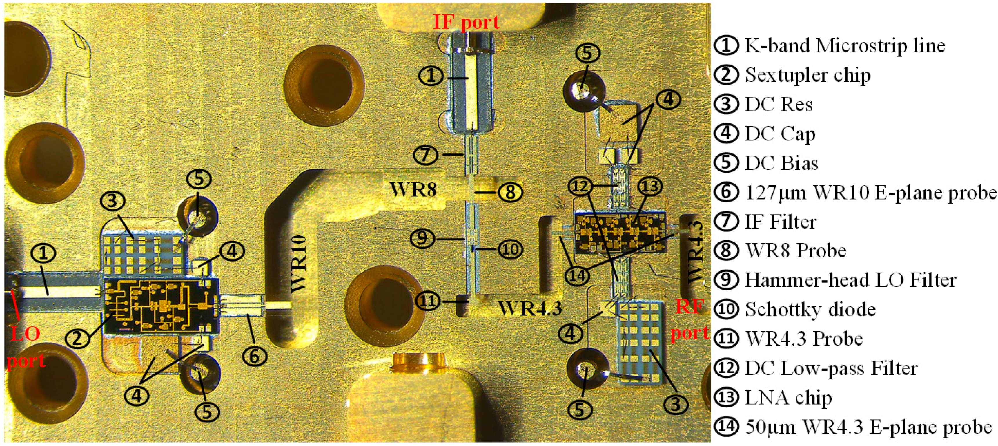
The design of the modules needs to address numerous structural challenges. The signal in the terahertz band only flows through a waveguide with little transmission loss; hence the three main functional components provided above employ waveguide connectivity. However, the output waveguide of the sextupler is a WR10 waveguide (2.54 mm × 1.27 mm) that is gradually reduced in height to become a WR8 waveguide (2.032 mm × 1.016 mm) in order to achieve the optimum impedance match for the mixer input. The RF input waveguide of the mixer is a WR4.3 waveguide (1.092 mm × 0.546 mm), which is the same as the output waveguide of the LNA. The entire cavity is then simulated in order to determine whether the combination of cavities will result in a resonant response. In addition, a 1000 pF capacitor and two 100 pf capacitors and voltage distribution resistor are arranged directly in the resonant cavity of the sextupler, in the same cavity as the chip but without resonance. However, the same number of capacitors and resistors placed in the resonant cavity of the LNA chip will produce resonance since the low noise amplifier operates in the G-band. Therefore, the resonant and supply cavities of the low noise amplifier are independently isolated, and each cavity is transferred to the DC supply via low pass filters. Additionally, some absorbent material has been installed on the top of the chip cavity in the appropriate location to avoid excessive resonance. A microstrip line is used to connect the coaxial connections for both the LO input and the IF output, and it has good transmission capability at frequencies below 20 GHz. The RF input port uses the same WR4.3 standard rectangular waveguide flange as the antenna.
Figure 6 depicts a picture of the G-band receiver module’s internal interconnection arrangement.
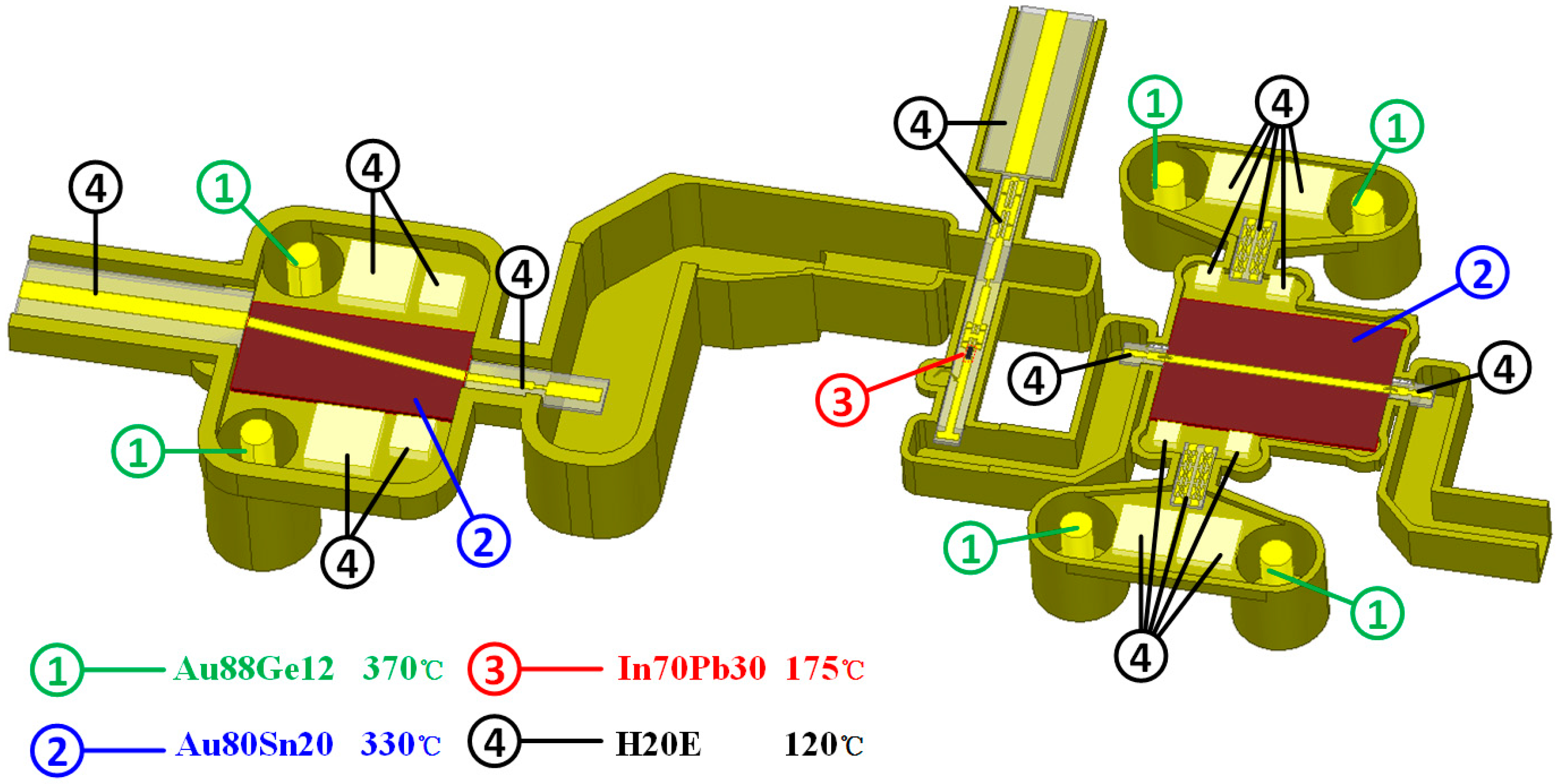
Due to their different levels of heat tolerance, Schottky diodes and MMICs require solders with differing melting points during the micro-assembly process. The recommended solder for each component is shown in
Figure 7. In order to bake and solder each component individually, the solders used in the micro-assembly must be arranged according to their melting points, starting with the highest melting point and going downward. The Au88Ge12 solder, having a melting point of 370 °C, is first used for soldering the DC insulator to the cavity. The second stage involves using Au80Sn20 solder with 330 °C melting temperature to solder the two chips to their respective locations in the cavity. Additionally, using the In70Pb30 solder with a melting point of 175 °C, the Schottky diode is attached to the appropriate location on the mixer substrate. In the following phase, electrically conductive silver epoxy (H20E), with a melting point of only 120 °C, is used to bond the capacitor and the complete substrates in the designated position. After all parts have been soldered and baked, the input and output ports of active chips are linked to the transmission substrates using gold wire bonding. The insulators and capacitors are connected by 100 μm wide gold tape to provide DC power to the chip.
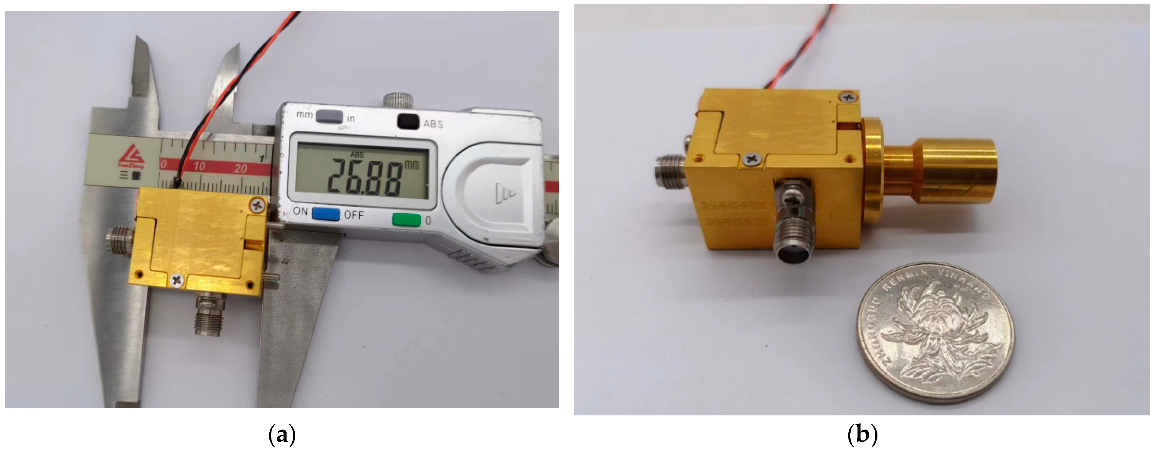
In addition, the module has a power-supply secondary-voltage-stabilizing circuit installed inside of it that powers the two active chips. When the circuit is fed with only +8 V DC, the circuit is able to provide both 4 V and 1.2 V positive and −0.3 V and −0.35 V negative power for the two active chips. During typical module operation, the total module current fluctuates between 110 mA and 116 mA, resulting in overall power consumption of the receiver between 0.88 W and 0.93 W. Finally, the size of the G-band receiver module (excluding the coaxial connectors) is only 27 × 20 × 20 mm
3, as shown in
Figure 8.


 ,
, 


