1. Introduction
In the past five decades, broadband mobile networks have experienced accelerated growth, culminating in the development of 5G networks. Current and future mobile networks, such as 5G and beyond, face technological challenges that include low latency, high data transfer rates, and extensive area coverage. The area coverage is dependent on the frequency used by operators for deploying their wireless networks and devices. While coverage may be limited to a short range, operators compensate by implementing numerous small cells with a lower-complexity design [
1].
This evolution requires an efficient and cost-effective solution for optical wireless front ends. To meet this need, information delivered by mobile stations is repeated over a distributed antenna system (DAS) that employs remote antenna units (RAUs) integrated with optical and wireless modules. These RAUs are used for mobile communications, as well as Internet of Things (IoT) devices and wireless sensor networks (WSNs).
To deploy a large number of terminal devices, the DAS interconnects with high-density remote access units [
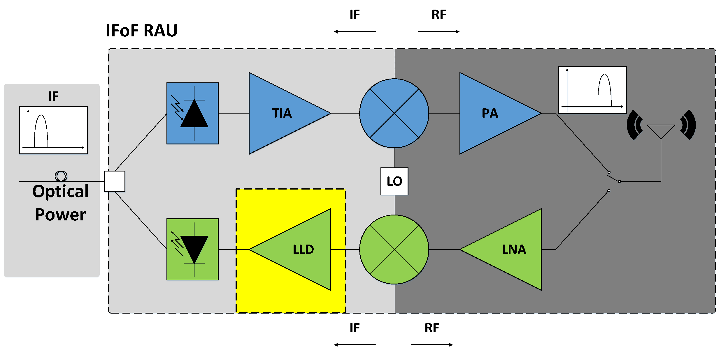
2]. The block diagram structure of an RAU is shown in
Figure 1. In terms of information representation, there is an alternative way to transmit information from a base station (BS), even if the wireless protocol establishes a digital modulation format with an analog representation of binary states that change only the phase—or both the phase and amplitude—for a particular binary symbol. The objective is to avoid the need for signal demodulation. On the contrary, the signal received from the BS is retransmitted, maintaining the same format.
These technologies are generally referred to as radio over fiber (RoF), with a specific approach known as intermediate frequency over fiber (IFoF) [
3]. The inclusion of an RF linear laser driver is fundamental in order to reach an optical power at the output of the light source that follows the form of the analog’s input signal.
Unlike other systems, the IFoF uplink does not require a modulator/demodulator pair to recover baseband information. Instead, the system shifts the frequency from RF to IF before transmitting the same analog signal over an optical fiber. After the block down-converter, a laser driver is required to produce the optical power output, as the light source operates in an electric current range [
4]. In the RAU, the highlighted yellow block represents the light source driver. This block generates a sufficient amount of electric current to produce optical power. Therefore, there is a correlation between the type of light source, the transmission mode over the fiber link, the use of single-mode or multi-mode optic fiber, and the modulation method of the light source.
Analog wide-band transmission systems utilize high-radiance light-emitting diodes (LEDs) and laser diodes, such as vertical-cavity surface-emitting lasers (VCSELs), which are accompanied by blocks to compensate for any non-linearities exhibited by these devices, as shown in
Figure 1, corresponding to the IFoF RAU scheme. The uplink is composed of an electro–optics interface that transmits information from remote terminals to the base station through an optical fiber.
In terms of the IFoF RAU operation, there are two possibilities for modulating the light source. This choice largely depends on how information is represented. In most cases, information is encoded in a digital format, enabling the configuration of an optical transmission system, where bits are represented as light pulses in their simplest form. This holds true regardless of whether the light source is configured for direct or external modulation. However, in many optical front ends, an external modulator is employed when the information is in the form of bits. This approach increases the complexity of electronic block fabrication compared to directly modulating the light source.
In an analog system, a time-variant electric analog signal,
, directly modulates a light source around the bias current point,
. When there is no signal input, the optical power is
. However, when a signal,
, is applied, the optical output power can be determined as follows:
The variable
m represents the modulation index (or modulation depth), which is defined by Equation (
2). The mathematical definition of the modulation index is depicted by the slope shown in
Figure 2 [
5]. It is important to note that for LEDs,
is defined as
, while for laser diodes,
is defined as
. Additionally,
represents the variation of the current around the bias point.
Initially, LEDs can be the preferable choice for analog applications because their output is directly proportional to the drive current. However, an increase in temperature affects the LED junction, causing it to operate in the non-linear region and introducing distortion. An alternative option is to utilize injection lasers operating above the threshold current, which provides a more suitable option for analog transmission compared to LEDs. However, mode instabilities can occur in the linear region, resulting in kinks observed at the laser output. In such cases, the utilization of single-mode light sources offers better linearity for the direct modulation of analog signals.
The non-linear response from a light source is a major problem for analog signals compared to digital signals. Non-linearity causes signal dispersion, altering the shape of the signal. To address this issue, there are several options for IC electronic designs to interact with the optical source. A cost-effective option is the use of an analog linear drive circuit that delivers a certain amount of electric current corresponding to an analog voltage input signal. This work presents the design and integration of an analog linear laser driver integrated circuit (IC) using 65-nm CMOS technology.
This paper is sequentially organized into several sections. Firstly, we provide explanations for the fundamentals and operation of the laser driver as part of the optical transmitter. In section two, we present detailed considerations regarding the main design of the linear laser driver. In section three, the procedure to integrate and characterize the linear laser driver (LLD)-integrated circuit is presented. In section four, the experimental results are summarized, along with a technical comparison of this work with other previously developed approaches. Finally, the main conclusions of the work will be presented.
2. Linear Laser Driver Design
An analog laser driver has important requirements for proper operation. That is why the laser driver inside the RAU scheme plays a fundamental role as the electronic block in the transmitter. Its main function is to take an information voltage signal and convert it into an analog modulation current suitable for the VCSEL direct modulation scheme [
6]. Several specifications are necessary for ensuring adequate operation. However, the most important factor is to deliver a highly linear response. This means that for a given input signal, the output should correspond to the same form as the input. It should not matter if the block provides some gain that compensates for losses introduced by impedance adaptation and wire connections.
The criteria mentioned above lead to certain requirements during the design of an analog laser driver. The reduction in transistor dimensions required to achieve a high-frequency response also leads to a lower breakdown voltage, making it more difficult to maintain an appropriate dynamic range voltage across the laser. This presents a challenge for new optical transmission systems, especially those using IFoF technology [
7].
As shown in
Figure 2, the expected behavior of direct modulation in a VCSEL focuses on the linear response at the output. This means that a diminished swing of the input signal should produce proportional optical power, and both transient and response frequencies should be analyzed.
The objective of designing a linear laser driver is to achieve a gain value of above 10 dB for an IFoF operation bandwidth, with an upper-frequency limit set to 500 MHz. Several experimental works have successfully demonstrated this capability in indoor DASs that support 4G LTE-A and 5G mobile services [
8].
The input and output impedance of the laser diode are both approximately 50
, given that they have a direct connection to other blocks. It is mandatory to include a control feedback loop to ensure a constant electrical current output, which can correct for any variations due to temperature changes or the aging of the VCSEL [
6,
9].
The design of a linear laser driver is required to maintain the injection current of a VCSEL, independent of temperature. To achieve this, the VCSEL must be biased by a high-impedance current source that provides a current above the threshold current. The VCSEL operates in the linear region for suitable analog modulation, and the LLD drives the current between maximum and minimum values. The optical output power level typically varies from 1 to 10 mA. Therefore, the LLD needs to swing the bias current in order to enable direct modulation through an analog input signal, ensuring optical transmission with different amplitudes and frequencies [
10].
Another crucial consideration is the need for the linear laser driver to establish an optimal impedance coupling with the VCSEL while maintaining an appropriate bias level. This is because commercial VCSELs typically have a dynamic resistance of 50 for a bias current of around 10 mA, necessitating an impedance matching between the LLD and the light source. Furthermore, it is preferable to achieve optimal performance from the laser without implementing a power-hungry control loop stage.
The structure proposed in this work is based on two degenerated differential pairs. This structure is commonly employed in many electronic designs due to its reliability in terms of linearity. It reduces the dependence on the transconductance of transistors by incorporating degeneration resistance. As a result, the gain can be expressed mathematically with two variables: the values of the load and source resistors. The linear behavior of the degenerated differential pair makes it well-suited for use as a laser driver. The gain of a degenerated differential pair is defined in the literature as follows, where R
D represents the drain resistor and R
DEG represents the degenerated resistor:
The objective is to design transistors with dimensions that yield a sufficiently high transconductance, g
m, allowing us to neglect the second term in the denominator of Equation (
3). As a result, the gain expression simplifies to a linear dependence on the drain resistor and degenerated resistor, as defined in Equation (
4), where
is typically between 1.5 and 2.
A current mirror is used to provide a fixed current for transistor biasing, which results in a stable operating point and a wide dynamic range for the input voltage. The laser driver schematic is shown in
Figure 3, with a differential method of driving a laser diode.
The schematic features n-MOS transistors that set the biasing point and common mode at half the value of the supply voltage (1.2 V). The first stage has a high gain and the second stage has an output impedance of 50 . Under these conditions, the biasing of the two stages compromises the DC response, and it is desirable to bias the second stage with the output of the first.
In the first stage, the dimensions of transistors M1 and M2 are set to W = 50 m with a channel length of L = 250 nm, arranged in a four-finger configuration. The drain resistor RD takes a value of 1 k, and the degeneration resistor RDEG is set to 50 . The second stage is very similar to the first, with the only difference being the dimensions of transistors M5 and M6, which are set to W = 200 m with a channel length of L = 140 nm. They are physically arranged in an eight-finger configuration, and both the drain and degeneration resistors have a value of 50 .
3. Integration and Characterization Setup for the LLD
The workflow for testing and measuring IC blocks consists of static and dynamic measurements [
11]. For the LLD, an important block is the current mirror design, as it provides a bias current for both stages through an applied voltage at the gate, fixing the transistor’s operating point to the saturation region. This helps to limit drain current variation and achieve a high common-mode rejection ratio (CMRR). A technical specification scheme is presented in
Figure 4. Additionally, resistance values are specified for both degeneration (R
DEG) and drain (R
D) resistors, which determine the gain, as defined in Equation (
4). To evaluate the nonlinear distortion, total harmonic distortion (THD) is computed by measuring the amplitude and frequency at the output, with a correct setup for visualization in an oscilloscope.
The frequency response considers the VCSEL input impedance as a load of the LLD. This means the usage of an equivalent circuit for the injection laser, resulting in more precise results that are presented in the following sub-section.
Another important aspect involves specifying the process design kit (PDK) for the 65-nm CMOS technology. More specifically, the process corresponds to TSMC 65 nm CMOS LOGIC_RF 1P9M (single poly and nine metal layers), salicide, Cu technology. This process utilizes standard n-channel MOS transistors, and the threshold voltage is computed by the simulator. It operates with a supply voltage of 1.2 V. The minimum channel length is 60 nm, and N+ poly resistors without salicide are employed. The model operates with a nominal temperature of 25 °C.
The laser driver integration combines both differential pairs into a single layout design, with the dimensions of the LLD being 70 µm by 80 µm, as presented in
Figure 5.
3.1. IC Dice Encapsulation
The linear laser driver integrated circuit was fabricated into a multi-project wafer (MPW). This integration requires a preliminary simulation that accounts for all parasitics occurring in pads, particularly in the metal paths of signal connections. Subsequently, the design is delivered to the foundry, providing all the connection specifications, including pin assignments for the pads.
The dimensions of the linear laser driver are 562 × 722 µm, including bond pads. Within a reserved area of 4 mm2 in the multi-project wafer, it is possible to accommodate other designs. Hence, it is imperative to optimize connections, such as sharing a pad for bias that maintains a consistent DC voltage value, and consider potential scenarios for test bench characterization and hardware design. The input and output differential signals play a crucial role, not only in simulations but also in the layout design. By ensuring symmetrical metal paths, we effectively minimize phase shifts.
3.2. Hardware Design
To characterize LLD, it is necessary to design and mount a printed circuit board (PCB) with appropriate connectors for input–output signals, bias pins, and signal–probe connectors. Another crucial hardware design constraint is to ensure that the microstrip is characterized with an impedance of 50
to match the impedance of the vector network analyzer (VNA) and oscilloscope in the test bench.
Figure 6 illustrates the schematic for the hardware design, including capacitors for filtering any radio-frequency signals in the laboratory and coupling capacitors for filtering AC from DC offset differential signals.
Note that the test bench configuration establishes a differential input–output signal, regardless of other passive or active elements used to combine those signals. It is important to select an appropriate VNA and oscilloscope to maintain the original simulation setup during the characterization procedure.
3.3. Linear Laser Driver PCB for Characterization
After completing the hardware design, the PCB for the LLD test bench setup is mounted. Prior to this, verification of connectivity and microstrip path continuity was carried out between common connection points. It is important to note that the ground reference was not limited to a single pin; in order to mitigate electromagnetic and radio-frequency interference, all relevant elements acting as antennas share the same ground reference, including those associated with measurement equipment. The final hardware setup is presented in
Figure 7, which highlights the LLD chip and all the auxiliary elements discussed in previous sections.
4. Results
In the laboratory, before proceeding with static and dynamic characterization, it is mandatory to follow an orderly task procedure to prevent any potential hardware damage caused by manual handling or excessive bias current. According to this mention, the first step is to bias the PCB using a DC power supply equipped with power-meter functionalities. This enables checking the current required by the LLD chip and auxiliary elements. The following sections present the main results of the LLD characterization.
4.1. Frequency Response
A critical parameter to evaluate is the frequency response and the bandwidth measured at the half-power point. As mentioned in previous paragraphs, the LLD is designed to operate with IFoF technologies.
Figure 8 displays a gain of 12.3 dB for a differential output. This measurement was conducted at the Wallonia Electronics and Communications Measurements Platform (WELCOME), located at the Institute for Information and Communication Technologies, Electronics, and Applied Mathematics (ICTEAM) of the Catholic University of Louvain. The WELCOME platform is equipped with a Keysight Technologies four-port VNA model N5242B PNA-X Microwave Network Analyzer, which has a frequency range of 10 MHz to 26.5 GHz in its standard configuration and supports balanced measurements.
Figure 8 displays the post-layout simulation frequency response labeled as S
21dd, post-simulation. It is worth noting the utilization of the BSIM4.6.1 model for simulations, ensuring more accurate results at the schematic level, post-layout instances, and bench-probe simulations. The latter emulate characterization measurements.
Additionally, to obtain accurate measurements in balanced VNA configuration, an electronic calibration kit N4691B helps to mitigate systematic errors caused by cable movements, defining the reference plane to SMA input–output connectors. Cable movements can introduce uncertainties and affect the accuracy of measurements, particularly when using an open-ended coaxial probe. The calibration kit is specifically designed to provide precise and reliable calibrations for coaxial measurements [
12].
The experimental S
21dd trace is presented in
Figure 8. The measured bandwidth result reaches 415 MHz, which is above the frequencies required for IFoF, 100–300 MHz [
13].
4.2. DC Response
There is a correlation between the linearity of the light source and the DC response of the linear laser driver. However, a practical method to determine the DC response of the LLD is to administer a swing of the direct current voltage, so as to probe the response of the LLD structure, taking into account the DC operating point and the cutoff and saturation regions of the n-MOS transistors. The voltage input signal can range from 0 V to 80 mVpp, ensuring a linear operating point and preventing distortions at the output of the LLD.
In the previous paragraphs, the correspondence between the optical power output and the bias current for a VCSEL light source was explained.
Figure 9 demonstrates a linear response within a specific voltage range, achieved by operating the n-MOS transistors in the saturation region.
4.3. Time Response
Transient analysis is a convenient method for verifying whether the output signals are distorted. Additionally, it enables us to determine if the output reaches 1.2 volts, which is the maximum DC level for a 65-nm CMOS.
Total harmonic distortion (THD) is a common method used to measure the level of non-linear distortion present in the output signal of an electronic amplifier. THD can be affected by various factors, such as the design of the amplifier, the load impedance, and the input signal level and frequency.
While the time representation of input and output signals is helpful for visualizing the presence of distortion at the output, THD measurement enables us to understand whether any of the corresponding harmonics contribute to distortion in the operation of the LLD.
To quantify linearity, THD measurements were conducted for five different frequencies and amplitudes. This allows us to observe the performance of the LLD across various setups and configurations, where the influence of second- and third-harmonic components can affect the shape of the output response signal. The results are presented in
Figure 10. The experimental setup consists of connecting the LLD differential output directly to an oscilloscope, which generates the signal itself, thereby reducing the influence of additional connectors and impedance mismatches.
5. Discussion
The experimental results for LLD design and implementation show great promise in terms of frequency response, linearity, and power consumption. It is crucial to establish a comparison with similar works at this stage, to define a research direction for introducing improvements and advancing toward the integration of this cell into a specific remote antenna unit, as explained in the introduction.
Currently, the literature presents various designs of laser diode drivers, primarily focusing on digital transmission as a common application. However, with the evolution and deployment of radio over fiber technologies, there is a growing demand for integrating new analog cells, specifically for intermediate frequency over fiber applications.
The implementation of linear laser drivers poses a significant challenge for future analog electronic designs. This is because any analog baseband or modulated signal can be retransmitted using an intermediate frequency over fiber (IFoF) configuration, where the output optical power exhibits an analog swing when a linear laser driver is employed.
In
Table 1, several significant reported laser drivers are listed for comparison. It is important to note that this particular work is innovative. It is the only laser driver that operates in a linear regime, the others operate in commutation. Therefore, the proposed laser driver is the only one suitable for IFoF links. It emphasizes low power consumption, cost-effectiveness, and excellent linearity performance.


