Article

Design and Validation of a V-Gate n-MOSFET-Based RH CMOS Logic Circuit with Tolerance to the TID Effect

1
Korea Atomic Energy Research Institute, Jeongeup 56212, Republic of Korea
2
Department of Electronic Engineering, Jeonbuk National University, Jeonju 54896, Republic of Korea
*
Author to whom correspondence should be addressed.
Electronics 2023, 12(15), 3331; https://doi.org/10.3390/electronics12153331
Submission received: 20 June 2023 / Revised: 1 August 2023 / Accepted: 2 August 2023 / Published: 3 August 2023
(This article belongs to the Special Issue Advanced CMOS Devices)

Abstract

:
This study designed a radiation-hardened (RH) complementary metal oxide semiconductor (CMOS) logic circuit based on an RH variable-gate (V-gate) n-MOSFET that was resistant to the total ionizing dose (TID) effect and evaluated its tolerance to radiation. Among the different CMOS logic circuits, NOT, NAND, and NOR gates were designed using V-gate n-MOSFETs by employing layout transformation techniques and standard p-MOSFETs. Before the process design, we predicted the radiation damage using modeling and simulation techniques and validated the tolerance by conducting actual radiation tests after the process design. Furthermore, we implemented the CMOS logic circuit process design in a 0.18 µm CMOS bulk process. The actual radiation test applied a total cumulative radiation dose of 25 kGy at 5 kGy per hour in a high-level gamma-ray irradiation facility. Consequently, the resistance of the RH CMOS logic circuit based on the RH V-gate n-MOSFET to the TID effect was validated through experiments.

1. Introduction

The logic circuit is the fundamental unit in semiconductor-based electronic devices used in radiation environments, such as the online monitoring systems of nuclear power plants, field-programmable gate arrays (FPGAs) [1], digital signal processors (DSPs) [2], and aerospace memory integrated circuits. These devices perform various functions, such as charge pump circuits, power management circuits, and I/O ports [3]. Logic circuits, which comprise a complementary metal oxide semiconductor (CMOS), are susceptible to cumulative radiation effects known as total ionizing dose (TID) effects, which can lead to data conversion errors, timing issues, and increased power consumption [2,3,4,5,6]. Therefore, a radiation-hardened design of the fundamental unit of electronic devices, that is, the logic circuit, is crucial. Furthermore, by ensuring radiation hardness at the basic unit circuit level, radiation-hardened designs for complex system-level circuits can be achieved.
When constructing CMOS logic circuits in sub-micron processes, p-MOSFETs are unaffected by TID effects. However, n-MOSFETs experience TID effects and generate trapped charges in the shallow trench isolation (STI) oxide, leading to leakage currents [7]. Recently, significant research has been conducted on layout modification techniques targeting n-MOSFETs, which are particularly susceptible to TID effects. The layout modification technique resists the TID effect by simply changing the layout of a unit MOSFET while using an existing commercial process. This technique does not require an additional process because the existing commercial process can be used without modification. The ELT, DGA, L Style, and I-gate structures are representative examples of MOSFET structures with layout transformation techniques [8,9,10,11,12,13,14]. Among them, the RH variable-gate n-MOSFET, which is minimized in terms of its speed and area, provides various structural advantages to the design of RH circuits, considering that it can efficiently connect the electrodes of each device in the construction of a semiconductor integrated circuit (IC) [15]. Therefore, this study proposes an RH CMOS logic circuit that is constructed using n-MOSFETs with such structures, along with conventional p-MOSFETs. The RH CMOS logic circuit is predicted in advance for radiation damage through modeling and simulation techniques and is implemented as an actual chip through a 0.18 µm CMOS process. Furthermore, we perform a radiation exposure test with a cumulative radiation dose of a total of 25 kGy to validate the radiation tolerance of the implemented chip. The remainder of this paper is structured as follows: Section 2 introduces the proposed RH CMOS logic circuit and performs the modeling and simulation of the proposed RH CMOS logic circuit. Section 3 describes the chip implementation and experimental results of the proposed RH CMOS logic circuit. Finally, Section 4 presents the conclusion.

2. Proposed RH CMOS Logic Circuits

The main damage to the TID effect of CMOS logic circuits is caused by the leakage current, owing to the fixed charge generated in the isolation oxide of the n-MOSFET. Therefore, the fixed charge generated from the isolated oxide of the n-MOSFET should be reduced in an RH design of a CMOS logic circuit. This study proposes an RH CMOS logic circuit structure using an RH variable gate (V-gate) n-MOSFET [15] and standard p-MOSFET to prevent these fixed charges. In this section, we describe the RH V-gate n-MOSFET resistant to TID effects and the proposed RH CMOS logic circuit structure. Subsequently, the RH CMOS logic circuit based on the RH V-gate n-MOSFET is modeled in a 3D structure using a technology computer-aided design (TCAD) tool. The modeled RH CMOS logic circuit simulates the damage caused by the TID effect and the results are analyzed and compared with the damage to a standard CMOS logic circuit.

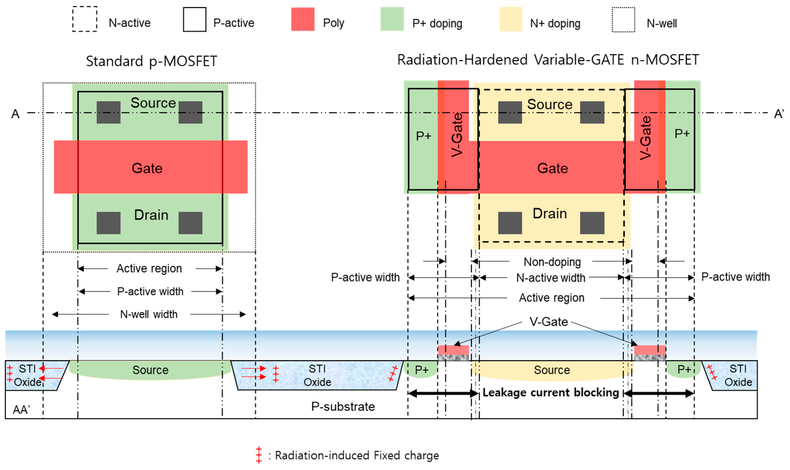
2.1. Introduction to the RH CMOS Logic Circuit

Figure 1 shows the basic configuration of the proposed RH CMOS logic circuit. The n-MOSFET and p-MOSFET in the CMOS are implemented as an RH V-gate n-MOSFET and Standard p-MOSFET, respectively. A-A′ show respective cross-sectional views. When radiation is incident on a CMOS, it undergoes the following four physical processes. First, it forms electron–hole pairs in the oxide layer. Electrons with a high mobility quickly escape the oxide layer, leaving holes with a slower mobility trapped inside the bandgap of the oxide layer. Second, the remaining holes trapped inside the bandgap move toward the silicon–oxide interface. Third, some of the holes get captured by Strained-Si bonds, owing to lattice mismatch, thereby generating fixed charges. Finally, charge carriers are induced by these fixed charges and accumulate. As a result, for n-MOSFETs, the Vth voltage decreases and the leakage current increases due to the fixed charges created in the gate oxide. Conversely, for p-MOSFETs, the Vth voltage increases due to the fixed charges in the gate oxide [16,17]. However, in the current sub-micron processes, where the gate oxide thickness is less than 10 nm, holes are not trapped in the gate oxide, but only in the STI oxide [17]. Therefore, for n-MOSFETs, the Vth voltage remains unchanged, owing to the TID effects; however, a leakage current occurs as a result of the accumulated holes in the STI oxide. For p-MOSFETs, the Vth voltage and leakage current do not change due to the TID effect; however, the drain current decreases due to radiation-induced short-channel effects [18]. This drain current reduction is almost negligible for the sizes of the p-MOSFETs used in logic circuits, and the p-MOSFETs used in CMOS logic circuits are relatively insensitive to TID effects. Therefore, by using a radiation-hardened (RH) n-MOSFET and standard p-MOSFET, an RH CMOS logic circuit can be constructed. In this study, a V-gate n-MOSFET was used as the RH n-MOSFET, which incorporates V-gate poly, P+ doping, and P-active layers to minimize the effects of the radiation-induced fixed charges present in the insulating oxide layer compared to the standard n-MOSFET, as shown in Figure 1. Through the V-gate poly, the leakage current path between the drain and source was blocked by replacing the thick STI oxide with a thin gate oxide on the drain and source sides. The threshold voltage was increased to prevent channel inversion caused by the fixed charges trapped in the silicon oxide and the generation of a leakage current by adding P+ doping and a P-active layer. Compared to the existing ELT, DGA, and I-gate layouts, it was minimized in terms of speed and area. By utilizing these principles, various structural advantages can be provided when configuring CMOS logic circuits with more efficient electrode connections of n-MOSFETs and p-MOSFETs, by adjusting the gate poly, p+, and p-active layer in various forms such as an I-shape, L-shape, C-shape, and Z-shape. Additionally, the channel size (W/L) of the device can be changed by adjusting the size of the RH layer. Therefore, radiation damage can be prevented regardless of the device size [11,15,19]. Unlike ELT and DGA n-MOSFETs, the W/L ratio of V-gate n-MOSFETs remains unchanged; therefore, the W/L size ratio must not be modified and process validation is possible during circuit design. Moreover, the V-gate poly-layer serves as a silicide-blocking layer to prevent band-to-band tunneling between the n+ and p+ layers. Owing to these advantages, the RH V-gate n-MOSFET and standard p-MOSFET can be used as the basic components to design logic circuits such as CMOS INV, NAND, NOR gates, and others.

2.2. V-Gate n-MOSFET-Based CMOS Logic Circuit Modeling and Simulation

The damage characteristics of the TID effect can be determined via irradiation experiments by designing a circuit and fabricating it into a chip. However, the process of conducting an irradiation experiment after circuit design and chip fabrication is expensive and time consuming, and radiation safety hazards are possible. In contrast, if the TID effects in semiconductors are modeled and simulated using software, the damage characteristics can be efficiently assessed without requiring extensive experimental testing. Consequently, the damage characteristics of the TID effect in the V-gate n-MOSFET-based CMOS logic circuit were evaluated using a TCAD tool. Furthermore, it was modeled according to the procedure shown in Figure 2, and the simulation results were analyzed.
To model the TID effect using the TCAD tool, a V-gate n-MOSFET-based CMOS logic circuit was first modeled in a 3D structure and its function was subsequently validated through a simulation. The characteristics of the TID effect were evaluated through simulations after modeling the fixed charge generated by the TID effect through ion implantation.
First, each RH CMOS logic circuit was modeled as a 3D structure, as shown in Figure 3. The NOT, NAND, and NOR gates are shown in Figure 3a,b, respectively. As shown in Figure 3b, it can be either a NAND gate or a NOR gate depending on the metal interconnections. The donor and acceptor concentrations of the RH V-gate n-MOSFET and standard p-MOSFET used in the logic circuit are shown in Figure 3c,d, respectively. The TID effect in the CMOS mainly results from the leakage current that occurs between the drain and the source of the n-MOSFET. Therefore, suppose that the leakage current path between the drain and the source of the n-MOSFET is blocked. Then, the CMOS becomes resistant to the TID effect. Using the aforementioned principle, RH CMOS logic circuits (NOT, NAND, and NOR gates) were constructed using RH V-gate n-MOSFETs. The channel size of the RH V-gate n-MOSFET used in the RH CMOS logic circuit was set to 2 µm/0.5 µm (W/L), the gate oxide thickness was 6.7 nm, and the body thickness was 3 µm. The doping concentrations of the substrate and channel were 2 × 10¹⁶/cm3 and 2 × 10¹⁶/cm3, respectively, whereas the doping concentration of the source, drain, and body was 3 × 10¹⁸/cm3. In the case of the standard p-MOSFET, the channel size was set to 4 µm/0.5 µm (W/L), and the gate oxide, body thickness, substrate doping concentration, channel doping concentration, source, drain, and body doping concentration were the same as those of the n-MOSFET. The n-well doping concentration was 3 × 10¹⁸/cm3. The characteristics of the modeled n-MOSFET and p-MOSFET refer to the CMOS 180 nm process.
To validate the functioning of the 3D-modeled RH CMOS logic circuit, the operating characteristics were checked with respect to time through a circuit simulation, as shown in Figure 4. For the NOT gate, an inverted output was obtained according to the input pulse. In the case of the NAND gate, logic “0” was output when the two inputs were high. In the case of the NOR gate, logic “1” was output when the two inputs were low. The RH CMOS logic circuit, which was modeled and validated for the operating characteristics, was compared and analyzed with a standard CMOS logic circuit to validate its effect on TID. Figure 5 shows the modeling of the fixed charge generated in the oxide layer of each n-MOSFET by the TID effect using the cutoff depth method [20]. The modeling of the TID effect of the standard CMOS logic circuit and RH CMOS logic are shown in Figure 5a,b, respectively. A-A′ and B-B′ show respective cross-sectional views. Currently, the doping concentration of the fixed charge injected into the oxide is 3 × 10¹⁸/cm3.
The damage characteristics owing to the TID effect of the standard and RH CMOS logic circuits were validated through circuit simulations, as shown in Figure 6. In the simulation, the standard CMOS NOT gate output of logic “1” decreased from 3.3 V to 2.51 V, the NAND gate decreased from 3.3 V to 2.22 V, and the NOR gate decreased from 3.3 V to 1.96 V, owing to the TID effect. However, unlike the standard CMOS logic circuit, the RH CMOS logic circuit was validated to have radiation resistance characteristics that showed the same results as those before the damage.

3. Chip Implementation and Experimental Results of RH CMOS Logic Circuit

For the RH CMOS logic circuit using the RH V-gate n-MOSFET, the damage to the TID effect was predicted in advance through modeling and simulation. In this section, the RH CMOS logic circuit was designed as an IC chip using KEY FOUNDRY’s 0.18 µm (STI) CMOS process to validate the actual damage characteristics of the TID effect. Additionally, the simulation results for the damage were obtained by modeling the leakage current flow owing to the TID effect. The circuit and IC chip were designed using the Cadence’s Specter and Virtuoso tools, which can be used to design circuits with process devices, create layouts, and can be validated. Subsequently, the operating characteristics of the fabricated chip were validated and an actual radiation experiment was conducted at the high-level radiation irradiation facility of the Korea Institute of Advanced Radiation Technology (ARTI). Finally, the radiation tolerance characteristics of the V-gate n-MOSFET-based CMOS logic circuit were validated.

3.1. Chip Implementation of the RH CMOS Logic Circuit

Two circuits were designed using KEY FOUNDRY’s 0.18 µm (STI) CMOS process to compare and analyze the actual damage characteristics of the RH CMOS logic circuit using the RH V-gate n-MOSFET with the standard CMOS logic circuit, as shown in Figure 7. The schematics of the NOT, NAND, and NOR gates, are shown in Figure 7a–c, respectively. The standard CMOS logic circuit and RH CMOS logic circuit are the same in terms of schematic representation, with the layout of the n-MOSFET being the only difference between the standard n-MOSFET and V-gate n-MOSFET. The channel sizes for the n-MOSFET and p-MOSFET in the NOT, NAND, and NOR gates are the same as the results obtained from the two models. The channel sizes for the n-MOSFET and p-MOSFET are designed as 2 μm/0.5 μm (W/L) and 4 μm/0.5 μm (W/L), respectively.
Figure 8 shows the layout of the RH CMOS logic circuit. Compared with the standard CMOS logic circuit, only the n-MOSFET was replaced with the RH V-gate layout-type n-MOSFET. In the CMOS structure, fixed charges in the STI oxide between the drain and source (n+) of the n-MOSFET and the n-well of the p-MOSFET can generate leakage current paths. These leakage current paths can be easily eliminated by using guard rings. Therefore, guard ring (p+, n+) techniques were applied to the n-MOSFET and p-MOSFET in the proposed RH CMOS logic circuit to prevent leakage current paths when fixed charges occur in the STI oxide between the drain and source (n+) of the n-MOSFET and n-well of the p-MOSFET.
Figure 9 shows the circuit simulation of the designed CMOS logic circuit with the leakage current flowing through. To simulate the leakage current flowing through the n-MOSFET owing to the TID effect, the n-MOSFET was modeled as a current source, whereas the resistance of the p-MOSFET when the n-MOSFET was OFF and the p-MOSFET was ON was modeled as a resistor for the circuit simulation. If a leakage current of 20 uA flows through the n-MOSFET when it is in the OFF state due to the TID effect, there will be a voltage drop in the product of the p-MOSFET’s on resistance and the leakage current for logic “1.” However, if no leakage current is flowing through the n-MOSFET, the voltage value of logic “1” will be maintained at the supply voltage of 3.3 V. Once the circuit design, layout, and simulation verification are completed, the chip manufacturing process will be carried out through semiconductor fabrication. Subsequently, the manufactured chip was implemented as a device under test (DUT) for electrical testing and radiation testing.

3.2. Radiation Exposure Test and Analysis of Results

The electrical characteristics were first determined to validate whether the CMOS logic circuits of the fabricated chip operated normally. The output was measured by applying square waves (0–3.3 V) of IN1 and IN2 with different cycles to the input terminal. Figure 10 shows the electrical characteristic output graph of the CMOS logic circuit. The output peak values of the standard and RH CMOS logic circuits operated normally at approximately 3.2 V and the initial peak values were validated.
Subsequently, an irradiation experiment was conducted to validate the TID effect in an actual radiation environment. The TID effect test was conducted at a high-level radiation facility at the Advanced Radiation Research Institute of Korea. Figure 11 shows the irradiation test setup. The test was divided into a control room that applied voltage to the DUT and measured the result through an oscilloscope, and an irradiation room that irradiated the cumulative dose to the test sample through a radiation source. For the irradiation test conditions, the dose was set to 5 kGy/h per hour, the total cumulative dose was set to 25 kGy, and the electrical data were measured by applying sinusoidal waves (0–3.3 V) to the input terminals IN1 and IN2 at different frequencies.
The experimental results are shown in Figure 12. After irradiation, the peak voltage of the standard CMOS NOT gate decreased from 3.221 V to 2.97 1 V, the NAND gate decreased from 3.231 V to 2.904 V, and the NOR gate decreased from 3.246 V to 2.51 V. This confirms that the radiation damage was caused by voltage drops of approximately 0.25, 0.33, and 0.74 V for the NOT, NAND, and NOR gates, respectively. In contrast, the peak voltage of the RH CMOS NOT, NAND, and NOR gates using the RH V-gate n-MOSFET ranged from 3.213 V to 3.211 V, 3.241 V to 3.24 V, and 3.255 V to 3.238 V, respectively, with a small voltage drop. In other words, the radiation resistance characteristics were validated. Additionally, as shown in Figure 13, when the leakage current was extracted, the general CMOS NOT, NAND, and NOR gates were approximately 11.52 µA, 13.05 µA, and 21.69 µA, respectively. In contrast, the leakage currents of the RH CMOS logic circuits were nearly unaffected by radiation damage, measuring approximately 10 nA, 34 nA, and 42 nA, respectively, in the order of tens of nanoamperes.
Table 1 summarizes the leakage currents flowing in the CMOS logic circuit owing to the TID effect. Unlike conventional CMOS logic circuits, the RH CMOS logic circuit exhibited minimal leakage currents owing to the TID effect. In this study, we validated the damage that occurred in standard CMOS logic circuits owing to the TID effect, as well as the radiation tolerance characteristics of RH CMOS logic circuits, using n-MOSFETs with RH V-gate layout structures. The CMOS logic circuits used in radiation environments are mainly used in various systems, such as DSPs or FPGAs, and tens of millions of logic circuits are used in one system. Supposed cumulative damage occurs in a CMOS logic circuit, which influences the next level, overlaps with the accumulated damage, and causes a malfunction of the system, such as timing errors or data errors. Therefore, the design of radiation-resistant CMOS logic circuits is crucial. As mentioned earlier, the V-gate layout structure is smaller and faster than structures that utilize other layout transformation techniques. Furthermore, by controlling the gate poly, p+, and p-active layer in various forms, such as an I-shape, L-shape, C-shape, and Z-shape, there are advantages in configuring CMOS logic circuits with more efficient electrode connections of the n-MOSFET and p-MOSFET. Additionally, this can ensure symmetry, making them robust against mismatches. Therefore, by merely altering the gate shape and adding a few layers, this technique becomes more radiation resistant and can be applied to existing processes, providing a distinct advantage compared to MOSFETs that use other layout modification techniques.

4. Conclusions

This study proposed an RH CMOS logic circuit for the radiation-resistant design of CMOS logic circuits, which are essential elements in most semiconductor ICs. The proposed RH CMOS logic circuit used the RH V-gate n-MOSFET based on the layout modification technique, which is resistant to the TID effect for the n-MOSFET constituting the CMOS. The RH V-gate n-MOSFET was minimized in terms of speed and area among the layout modification techniques and provided various structural advantages to RH circuit design, considering that the electrodes of each device can be connected more efficiently when configuring semiconductor ICs. A 3D structure was modeled and simulated using the TCAD tool to predict the damage characteristics of the TID effect before chip fabrication. The damage characteristics were modeled using the cutoff depth method for the fixed charges generated in the oxide layer of the n-MOSFET. The simulation results showed that, unlike the standard CMOS logic circuit, the radiation tolerance characteristics of the RH CMOS logic circuit were consistent with those before the damage. Upon the completion of the modeling and simulation, standard and RH CMOS logic circuits were designed using KEY FOUNDRY’s 0.18 µm (STI) CMOS process to validate the actual radiation damage characteristics of the RH CMOS logic circuit. Each circuit was designed using the Cadence and Specter tools and was finally implemented as an IC chip after the layout design and process validation. The normal operation of the fabricated IC chip was validated through an electrical characteristic test. A radiation irradiation test was conducted using a high-level gamma-ray irradiation device at the Korea Advanced Radiation Research Institute to validate the actual damage characteristics. Based on the experimental results, the RH CMOS logic circuit based on the RH V-gate n-MOSFET was found to be resistant to the TID effect, unlike the standard CMOS logic circuit. Finally, when the V-gate n-MOSFET with these advantages was configured as a CMOS logic circuit, the area of the system significantly decreased, the speed improved, and the leakage current was almost nonexistent, owing to the radiation resistance. This research was conducted with the aim of enhancing the radiation tolerance of the semiconductors used in radiation environments, such as space and nuclear power plants. Additionally, significant contributions are expected to achieve the anti-radiation of electronic systems in radiation environments by improving the area and speed of existing devices.

Author Contributions

Conceptualization, D.K. and N.L.; methodology, D.K. and S.C.; software, D.K. and M.L.; validation, S.C., D.K. and M.L.; investigation, D.K.; data curation, D.K. and M.L.; writing—original draft preparation, D.K. and M.L.; writing—review and editing, S.C. and D.K.; visualization, M.L.; supervision, S.C.; project administration, N.L. All authors have read and agreed to the published version of the manuscript.

Funding

This research was supported by the KAERI Institutional R&D Program (Project No. 523420-23). This research was supported by the IDEC.

Data Availability Statement

No new data were created or analyzed in this study. Data sharing is not applicable to this article.

Conflicts of Interest

The authors declare no conflict of interest.

References

  1. Huang, Q.; Jiang, J. An overview of radiation effects on electronic devices under severe accident conditions in NPPs, rad-hardened design techniques and simulation tools. Prog. Nucl. Energy 2019, 114, 105–120. [Google Scholar] [CrossRef]
  2. Xin, Y.; Wu, L.; Xiaolong, L.; Mohan, L.; Xin, W.; Jing, S.; Qi, G. Total Ionizing Dose Effect and Failure Mechanism of Digital Signal Processor. Chin. J. Electron. 2021, 32, 986–990. [Google Scholar] [CrossRef]
  3. Hu, Z.; Liu, Z.; Shao, H.; Zhang, Z.; Ning, B.; Chen, M.; Bi, D.; Zou, S. Total ionizing dose effects in elementary devices for 180-nm flash technologies. Microelectron. Reliab. 2011, 51, 1295–1301. [Google Scholar] [CrossRef]
  4. Li, J.; Chen, W.; Li, R.; Wang, G.; Qi, C.; Liu, Y.; Jin, X.; Bai, X.; Wang, C. Effects of total ionizing dose on transient ionizing radiation upset sensitivity of 40–180 nm SRAMs. AIP Adv. 2022, 12, 015026. [Google Scholar] [CrossRef]
  5. Gaul, S.; van Vonno, N.; Voldman, S.; Morris, W. Integrated Circuit Design for Radiation Environments; Wiley: New York, NY, USA, 2019. [Google Scholar]
  6. Dewitte, H.; Paillet, P.; Rizzolo, S.; Roch, A.L.; Marcandella, C.; Goiffon, V. Ultra-high total ionizing dose effects on MOSFETs for analog applications. IEEE Trans. Nucl. Sci. 2021, 68, 697–706. [Google Scholar] [CrossRef]
  7. Kumar, M.; Ubhi, J.S.; Basra, S.; Chawla, A.; Jatana, H.S. Total ionizing dose hardness analysis of transistors in commercial 180 nm CMOS technology. Microelectron. J. 2021, 115, 105182. [Google Scholar] [CrossRef]
  8. Chen, L.; Gingrich, D.M. Study of N-channel MOSFETs with an enclosed-gate layout in a 0.18 µm CMOS technology. IEEE Trans. Nucl. Sci. 2005, 52, 861–867. [Google Scholar] [CrossRef]
  9. Bucher, M.; Nikolaou, A.; Papadopoulou, A.; Makris, N.; Chevas, L.; Borghello, G.; Koch, H.D.; Faccio, F. Total Ionizing Dose Effects on Analog Performance of 65 nm Bulk CMOS with Enclosed-Gate and Standard Layout. In Proceedings of the International Conference on Microelectronic Test Structures, Austin, TX, USA, 19–22 March 2018. [Google Scholar] [CrossRef]
  10. Cardoso, G.S.; Balen, T.R. Performance Evaluation of Radiation Hardened Analog Circuits based on Enclosed Layout Geometry. In Proceedings of the 17th IEEE Latin American Test Symposium (LATS), Foz do Iguacu, Brazil, 6–8 April 2016. [Google Scholar] [CrossRef]
  11. Lee, M.S.; Lee, H.C. Dummy gate-assisted n-MOSFET layout for a radiation-tolerant integrated circuit. IEEE Trans. Nucl. Sci. 2013, 60, 3084–3091. [Google Scholar] [CrossRef]
  12. Lee, M.S.; Lee, H.C. Aspect ratio model for radiation-tolerant dummy gate-assisted n-MOSFET layout. Int. Sch. Res. Not. 2014, 2014, 145759. [Google Scholar] [CrossRef] [PubMed] [Green Version]
  13. Malik, M.; Prakash, N.R.; Kumar, A.; Jatana, H.S. L Style n-MOSFET Layout For Mitigating TID Effects; Springer: Silicon Valley, CA, USA, 2021. [Google Scholar]
  14. Lee, M.; Cho, S.; Lee, N.; Jeong, S.; Kim, S. Design of a radiation-tolerant I-gate n-MOSFET structure and analysis of Its characteristic. J. Korea Inst. Inf. Commun. Eng. 2016, 20, 1927–1934. [Google Scholar] [CrossRef] [Green Version]
  15. Lee, M.; Lee, N.; Kim, J.; Hwang, Y.; Cho, S. Modeling and simulation-based layout optimization for tolerance to TID effect on n-MOSFET. Electronics 2021, 10, 887. [Google Scholar] [CrossRef]
  16. Bala, S.; Kumar, R.; Kumar, A. Total ionization dose (TID) effects on 2D MOS devices. Trans. Electr. Electron. Mater. 2021, 22, 1–9. [Google Scholar] [CrossRef]
  17. Saks, N.S.; Ancona, M.G.; Modolo, J.A. Generation of interface states by ionizing radiation in very thin MOS oxides. IEEE Trans. Nucl. Sci. 1986, 33, 1185–1190. [Google Scholar] [CrossRef] [Green Version]
  18. Ogasawara, M.; Yoshida, R.; Oshima, Y.; Ando, M.; Kimura, A.; Hirakawa, K.; Lwase, M.; Nabeya, S.; Yoda, T.; Ishihara, N. Dependence of total ionizing dose effect of nMOS transistors on the on/off duty ratio of a gate voltage. Jpn. J. Appl. Phys. 2021, 60, 104501. [Google Scholar] [CrossRef]
  19. Malik, M.; Prakash, N.R.; Kumar, A. Comparative analysis of radiation tolerant analog circuit layout in 180 nm CMOS technology for space application. Microelectron. J. 2023, 131, 105665. [Google Scholar] [CrossRef]
  20. Turowski, M.; Raman, A.; Schrimpf, R.D. Nonuniform total-dose-induced charge distribution in shallow-trench isolation oxides. IEEE Trans. Nucl. Sci. 2004, 51, 3166–3171. [Google Scholar] [CrossRef]
Figure 1. Basic configuration of the proposed RH CMOS logic circuit.
Electronics 12 03331 g001
Figure 2. Modeling sequence of the TID effect.
Electronics 12 03331 g002
Figure 3. Three-dimensional structural modeling of a V-gate n-MOSFET-based RH CMOS logic circuit. (a) NOT gate, (b) NAND(NOR) gate, (c) donor concentration, and (d) acceptor concentration.
Electronics 12 03331 g003
Figure 4. Operating characteristics of the RH CMOS logic gate.
Electronics 12 03331 g004
Figure 5. Modeling of the TID effect of (a) a standard CMOS logic circuit, and (b) an RH CMOS logic circuit.
Electronics 12 03331 g005
Figure 6. TID damage characteristics of the standard and RH CMOS logic circuits.
Electronics 12 03331 g006
Figure 7. Schematic of the logic circuit (a) NOT gate, (b) NAND gate, and (c) NOR gate.
Electronics 12 03331 g007
Figure 8. Layout of the RH CMOS logic circuit.
Electronics 12 03331 g008
Figure 9. Circuit simulation result of the CMOS logic circuit.
Electronics 12 03331 g009
Figure 10. Electrical characteristic test of the fabricated chips.
Electronics 12 03331 g010
Figure 11. Irradiation test configuration.
Electronics 12 03331 g011
Figure 12. Radiation characteristics experiment.
Electronics 12 03331 g012
Figure 13. Actual measurement results of the leakage current of the CMOS logic circuit based on the cumulative dose.
Electronics 12 03331 g013
Table 1. Actual measurement results of the leakage current of the experiment on the TID effect.
TypeLeakage Current (@25 kGy)
Standard CMOS NOT [μA]11.52
Radiation-Hardened CMOS NOT [μA]0.01
Standard CMOS NAND [μA]13.05
Radiation-Hardened CMOS NAND [μA]0.034
Standard CMOS NOR [μA]21.69
Radiation-Hardened CMOS NOR [μA]0.042
Disclaimer/Publisher’s Note: The statements, opinions and data contained in all publications are solely those of the individual author(s) and contributor(s) and not of MDPI and/or the editor(s). MDPI and/or the editor(s) disclaim responsibility for any injury to people or property resulting from any ideas, methods, instructions or products referred to in the content.

