Abstract
The Cache plays an important role in computer architecture by reducing the access time of the processor and improving its performance. The hardware design of the Cache is complex and it is challenging to verify its functions, so the traditional Verilog-based verification method is no longer applicable. This paper proposes a comprehensive and efficient verification testbench based on the SystemVerilog language and universal verification methodology (UVM) for an instruction Cache (I-Cache) controller. Corresponding testcases are designed for each feature of the I-Cache controller and automatically executed using a python script on an electronic design automation (EDA) tool. After simulating a large number of testcases, the statistics reveal that the module’s code coverage is 99.13%. Additionally, both the function coverage and the assertion coverage of the module reach 100%. Our results demonstrate that these coverage metrics meet the requirements and ensure the thoroughness of function verification. Furthermore, the established verification testbench exhibits excellent scalability and reusability, making it easily applicable to higher-level verification scenarios.
1. Introduction
As the complexity of chips increases, the task of verifying their functionality becomes more challenging. Any abnormal function within a chip module can lead to system failure, emphasizing the need for robust chip verification methods. Among the critical modules in a processor chip, the Cache [1,2] plays a significant role by storing frequently accessed instructions or data. It possesses features such as a relatively small capacity and high speed. The Cache operates at a clock rate comparable to that of the processor, which is typically faster than the main memory. As a result, the Cache substantially enhances the processor’s performance. Given the intricate hardware design of the Cache, it becomes crucial to employ an appropriate function verification method to ensure its correctness.
In the work by Biswal et al. [3], system-level verification was conducted for the system on chip (SOC) where the Cache resides. However, more detailed and specific verification for the Cache module itself was not performed, creating risks for the entire SOC system. Simultaneously, the work also lacks an explanation of the reusability of the module-level verification testbench. In SoC systems, verification is typically conducted at various levels, progressing sequentially from low to high. The low-level verification testbench can be reused in the high-level verification testbench, necessitating the completion of module-level verification prior to system-level verification. The module-level verification testbench should possess good reusability to enable coupling with the system and verification testbench. Zhou [4] proposed a UVM verification testbench that does not include a reference model component. This testbench focused on module-level verification, specifically targeting the main function of each module, without utilizing assertions and other verification methods. The actual working scenario of a chip is complex, encompassing not only the main functional aspects but also incorporating abnormal working scenarios. These scenarios may involve timing relationships, interrupt responses, and other factors that need to be considered to achieve comprehensive functional verification. Kaur [5] designed a four-way set-associative Cache controller and performed functional simulation using an online simulator. While the simulation waveform for typical function points was provided, coverage statistics were not performed. This means there is a lack of quantitative indicators to measure verification completeness, which could potentially result in hidden design issues. Similarly, in the work by Omran et al. [6], the authors simulated their designed Cache using an emulator that accompanies the field programmable gate array (FPGA) device. This type of emulator supports fewer features and allows for the use of the Verilog language to build a simple verification testbench and develop directional excitation applied to the Cache. This approach aims to achieve functional verification. Although this method can verify the main functions of the Cache, it is challenging to cover all the working scenarios for the Cache to perform directional testing due to its incentive properties. As a result, the whole verification process fails to achieve good completeness. To summarize, in the current stage of research there is a lack of a verification testbench for Cache design with a complete verification scheme and high reusability. In order to achieve this goal, it is necessary to select appropriate tools and verification methods.
UVM is a verification framework based on the SystemVerilog language, which itself evolved from the Verilog hardware description language. SystemVerilog is fully compatible with Verilog and combines hardware design capabilities with software language characteristics, making it widely used in chip verification processes. SystemVerilog adheres closely to the principles of object-oriented programming (OOP) and incorporates most of the features found in object-oriented languages. This object-oriented approach brings several benefits when compared to traditional Verilog verification methods. The UVM verification testbench built on top of SystemVerilog offers strong reusability, a clear and organized structure, and high efficiency. In traditional Verilog verification, which is often based on directed testing, the focus is on verifying hardware designs with relatively simple structures and functions. However, UVM introduces a random verification strategy [7] that allows for scenario-based testing, allowing for the verification of various working scenarios of the chip. This approach significantly improves the completeness of the verification process. UVM is also evolving towards coverage-driven verification (CDV), where coverage metrics are used to evaluate the progress of verification. By setting coverage goals, engineers can ensure that the verification process comprehensively exercises different aspects of the design. One of the reasons UVM is an efficient verification methodology lies in its incorporation of special mechanisms. The sequence mechanism facilitates the generation of reusable stimuli, the phase mechanism provides a hierarchical structure for the simulation process, and the objection mechanism allows for control over the simulation termination. These features contribute to the efficiency of UVM in performing simulation verification, spanning from the module level to the system level in digital circuits [8].
In this paper, we build a coverage-driven verification approach based on the UVM testbench for the I-Cache controller. UVM, which inherits from the open verification methodology (OVM), is a next-generation verification methodology known for its efficiency and reusability. Specifically, random testcases are first developed to verify the general functional features of the module. During this process, function coverage groups are defined to ensure adequate coverage. For specific scenarios, directional testcases are developed to verify the normal functioning of the module, potentially targeting exception scenarios as well. Moreover, some temporal relationships are checked with SystemVerilog Assertions (SVA) [9] and assertion coverage is measured. Overall, this paper aims to leverage the advantages of the UVM verification testbench to enhance the completeness, reusability, and extensibility of the Cache function verification process, addressing limitations encountered by previous approaches.
2. Function of Design and Verification Plan
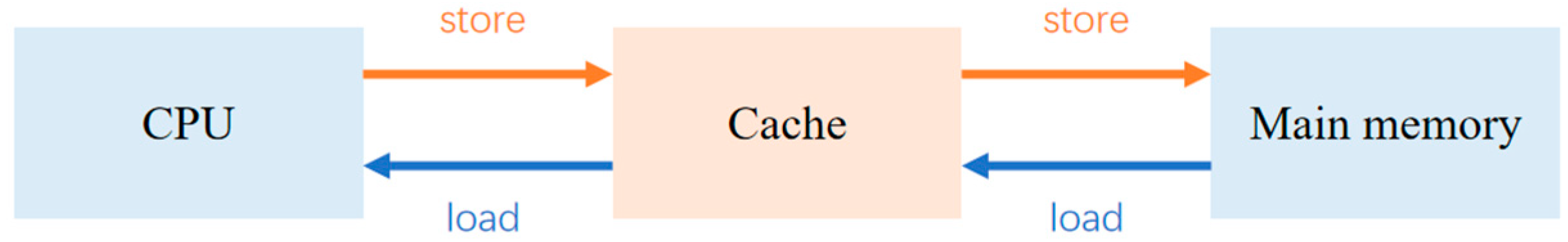
The data in the Cache is a copy of some of the data in the main memory. So, when the central processing unit (CPU) wants to use the data in the main memory, it can retrieve the required data from the faster Cache, resulting in reduced access time. The relationship between the CPU, Cache, and main memory is depicted in Figure 1. According to the theory of the Harvard structure, the first-level Cache is divided into an instruction Cache and a data Cache. These Caches are independent of each other and respectively store the instructions and data required by the processor. On the other hand, the second-level Cache does not make a distinction between instructions and data. In the context of the CPU accessing the Cache, if the required data are present in the Cache, they are referred to as a “hit”. Otherwise, they are referred to as a “miss”.
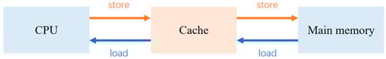
Figure 1.
Relationship between CPU, Cache, and main memory.
The I-Cache operates as a direct-mapped Cache in all Cache configurations. This means that each location in the system memory can reside in exactly one location in the I-Cache. Because the I-Cache is direct-mapped [10], its replacement strategy [11,12,13] is simple: each newly cached line replaces the previously cached line. The I-Cache is a non-blocking Cache [14], which means that multiple unprocessed misses are allowed, in which case a specific module is required to store the information of unprocessed misses.
2.1. Main Components of the I-Cache Controller
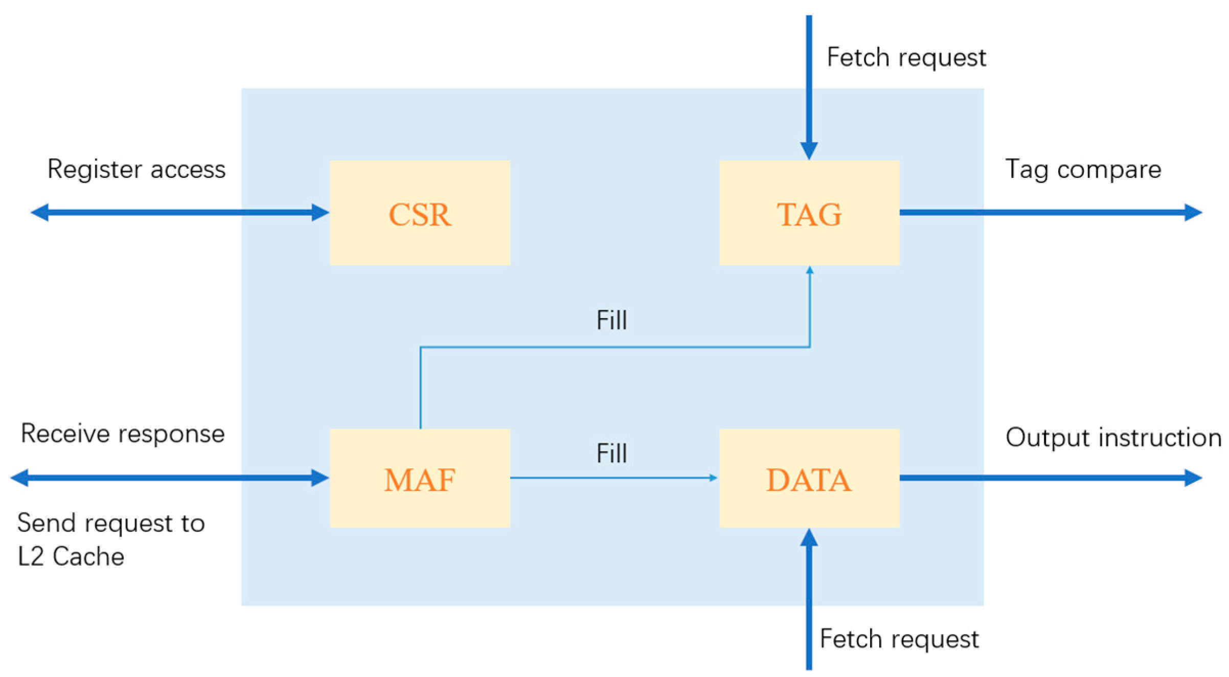
As is evident from the previous section, the controller interacts with data from multiple components. The register configuration channel originates from the load-store unit, which serves as the first component. Among the components, the CPU utilizes the instructions stored in the load-store unit. Furthermore, in the multilevel structure of the Cache, when the instruction Cache is unavailable, the controller initiates a request to the next level of memory, known as the L2 Cache. The structural block diagram of the I-Cache to be verified is shown in Figure 2. The CPU sends a fetch request to the I-Cache. If the tag comparison in the TAG module is successful, instruction data are output from the DATA module. The MAF module sends a request to the L2 Cache and receives the response. The registers inside the I-Cache are accessed via a register bus. More detailed descriptions are as follows:
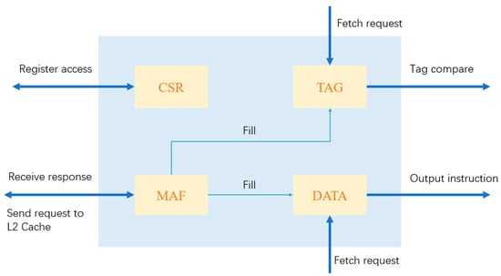
Figure 2.
Structural block diagram of the I-Cache controller.
- CSR: Control and status register. The registers inside the CSR module are configured through the configuration bus to support related functions. The definition of the registers are shown in Table 1.
 Table 1. Definition of registers.
 - MAF: miss addr file, which is also known as miss status handling register (MSHR). When a missing item occurs, the module saves the missing information, sends a request message to the L2 Cache, and waits for the L2 Cache to return the data. It contains four item units, and each item unit can save a missing message. It defines a pointer to control the switch of these four items. This module also populates the data it holds internally into the TAG module and the DATA module.
- TAG: The module consists of a tag storage unit and corresponding control logic. It fills the upper part of the address from the MAF into the tag storage, and completes the tag comparison when a fetch request arrives to determine whether the current access is a hit.
- DATA: The module consists of a data storage unit and corresponding control logic. Its primary function is to store data from the MAF and determine whether the accessed object is a Cache region or a static random-access memory (SRAM) [15,16] region based on the currently set Cache size.
2.2. Main Functions of the I-Cache Controller
The key functions of the I-Cache controller are as follows:
- The Cache size can be configured, including 0 kb, 4 kb, 8 kb, 16 kb, and 32 kb. The total storage space size is 32 kb. For example, when the Cache size is configured to 4 kb, the SRAM size is 28 kb.
- It supports freeze mode. The significance of the freeze mode is to protect the contents of the Cache under certain circumstances. If the Cache space is larger than 0 kb, no memory will be filled in the freeze mode even if a Cache loss occurs, which is normal when the freeze mode is disabled.
- It supports instruction prefetch. When the CPU initiates a fetch operation to the I-Cache (assuming the fetch address is addr), and the result of this operation is missing, the I-Cache sends a request to the L2 Cache, and the L2 Cache returns the data corresponding to the addr and the data of the addresses adjacent to the addr. The command prefetch improves the Cache system efficiency.
- It supports global and block invalidation operations. We can configure specific registers via configuration bus to complete the corresponding operation. If the Cache size is changed when the system is running, the global invalidation operation is triggered to avoid unnecessary errors.
2.3. Proposed Verification Plan
UVM excels in verifying digital circuit designs, particularly for complex circuits. Its advantages include improved reusability, organized structure, support for random verification strategies, and coverage-driven verification, making it a popular choice in the chip verification domain. The chip encompasses real-world working scenarios, and it is essential that we ensure the chip’s ability to function properly in various working scenarios. This includes both normal and abnormal scenarios, as well as boundary scenarios. Therefore, when formulating verification schemes, it is crucial to consider the aspect of completeness in verification. In this paper, diverse verification methods are employed to guarantee comprehensive verification.
- Common work scenarios
- Random testcases are designed for simulation verification. In the simulation process, the scoreboard will conduct a real-time data comparison (the two data sources are respectively from the reference model and the monitor monitoring DUT data). If the comparison fails, the corresponding error information will be printed in the simulation log, and the wrong data packet and its corresponding id will be given in detail.
- (1)
- CPU sequential fetch: The Cache size and freeze mode are randomly configured. The fetch address increases in sequence. Since the controller supports instruction prefetch functionality, the instructions corresponding to two adjacent addresses are retrieved sequentially.
- (2)
- CPU branch fetch: The Cache size and freeze mode are randomly configured. Fetch refers to the process of increasing the address sequence. When a branch address suddenly appears, it can result in the occupation of more items.
- Special work scenarios
- (1)
- CPU access times out: The item will be automatically released, which will result in a miss on the next fetch. Under normal circumstances, the current item is released when it is accessed successfully.
- (2)
- L2 Cache returns data in an out-of-order manner: During a sequential branch fetch, the instruction Cache sends two consecutive requests to the L2 Cache. Depending on the situation in the L2 Cache, it may not return the requested data in the expected order.
- SVA check
Special timing relationships are checked using SVA, and error messages are printed in the simulation log file when violations occur.
3. UVM Verification Testbench
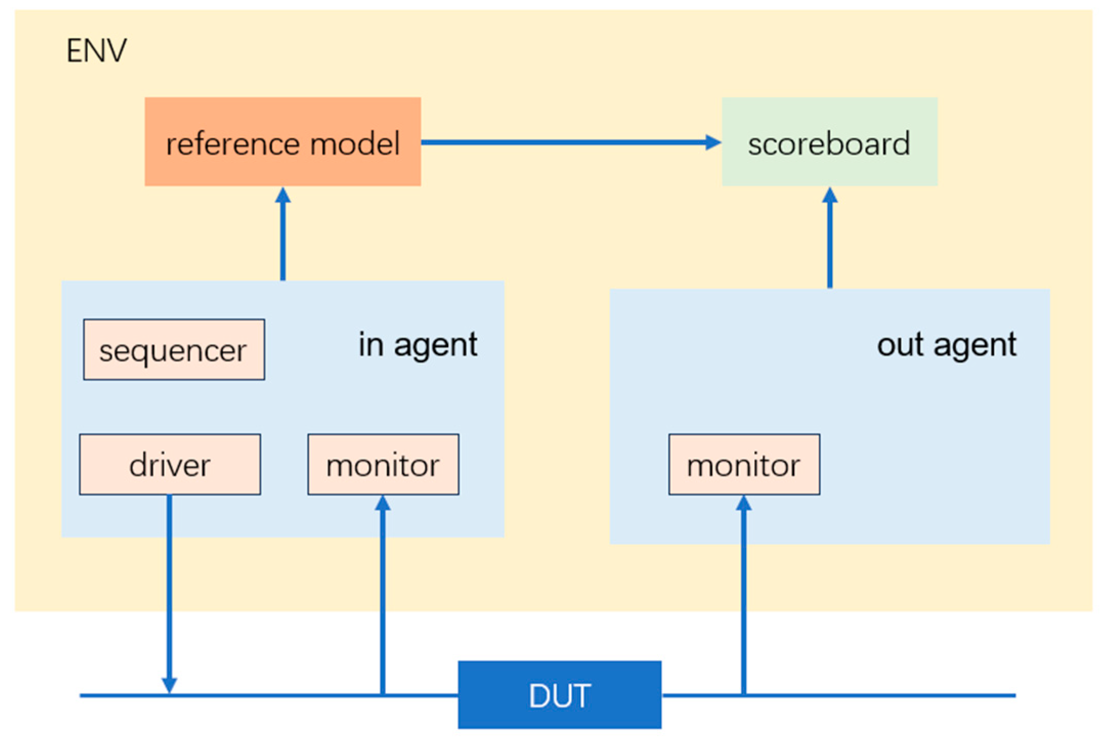
As shown in Figure 3, a basic UVM verification testbench is centered around the verification environment [17,18], which typically contains components such as agent, reference model, and scoreboard. In general, each agent represents a data protocol. The agent is connected to the DUT through an interface, and the components also establish the necessary connections to maintain data communication within the verification environment.
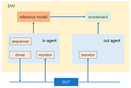
Figure 3.
The structure of a basic UVM verification testbench.
3.1. Architecture of the Verification Testbench
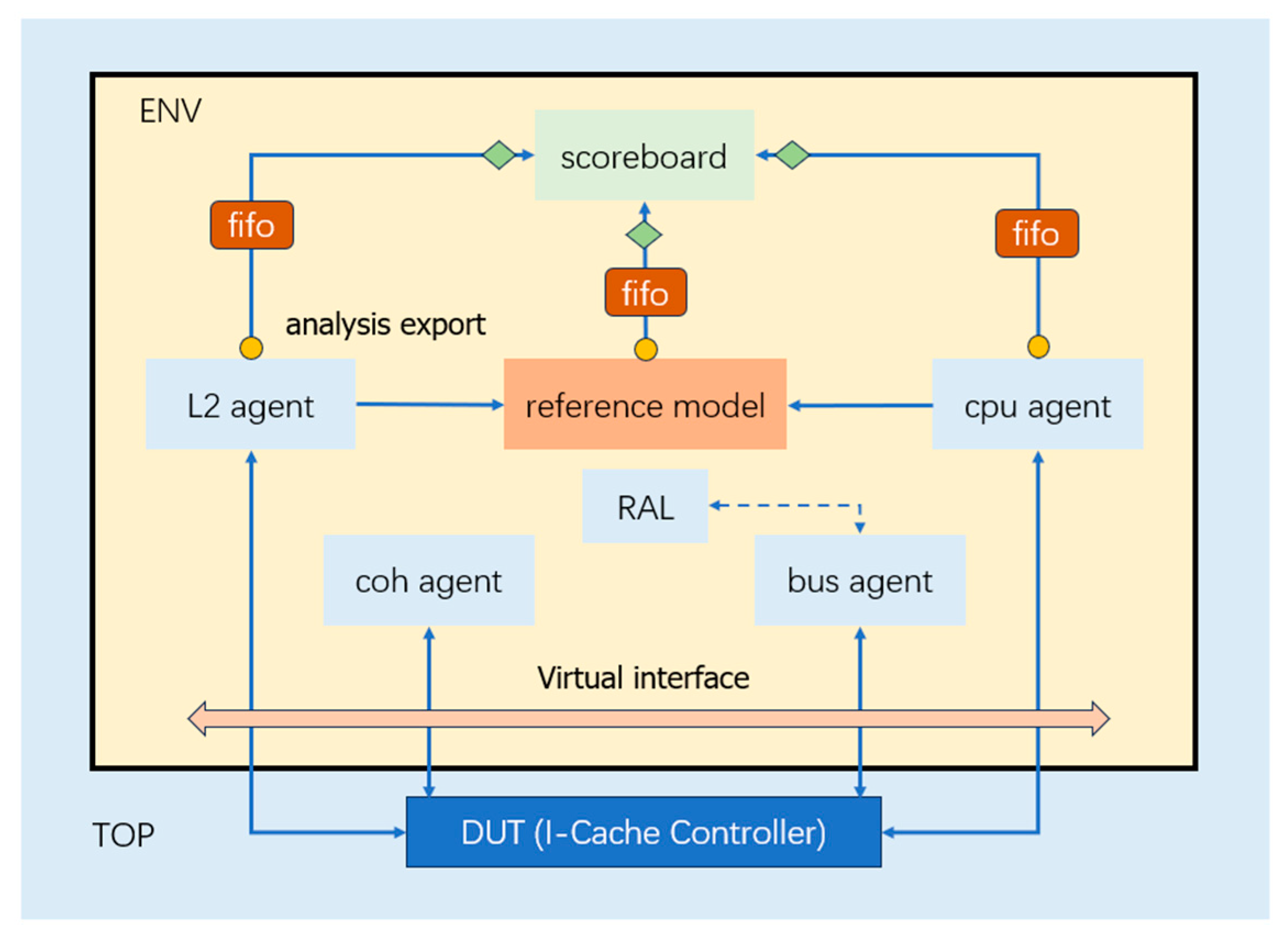
The verification testbench proposed in this paper is an extension of the previously shown verification testbench in Figure 3, and its architecture diagram is depicted in Figure 4. As discussed in Section 2, the registers in the Cache need to be configured through the register configuration bus to enable operations such as changing the Cache size and freeze mode. This functionality is implemented by the bus agent in the verification environment. When the CPU reaches the fetch pipeline [19], it initiates a fetch operation to the I-Cache. To simulate the CPU’s access to the I-Cache, the CPU agent is set up in the verification environment. In the event of a Cache miss in the I-Cache, a request is sent to the L2 Cache, and the system waits for the L2 Cache to return the data. Hence, an L2 agent is established to handle the I-Cache’s interactions with the L2 Cache. Additionally, a coherency (coh) agent is included to manage invalidations between the I-Cache and the L2 Cache. The register abstraction layer (RAL) [20] is an essential component of the verification environment, providing convenient access to registers through various methods. The verification environment includes an essential component known as the reference model [21], implemented using a software language to achieve the same functions as the hardware design. During the random test phase, the reference model plays a crucial role in verifying the logic of the I-Cache by comparing the data from the I-Cache with the data from the scoreboard [22]. The scoreboard, being the final component in the verification environment, automatically performs data comparisons.
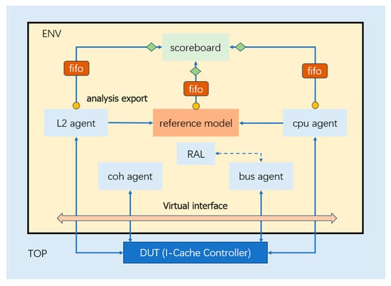
Figure 4.
The architecture of the proposed verification testbench.
TOP is the top layer of the verification testbench, where the DUT is instantiated and the verification testbench is started by the UVM’s built-in function run_test(). ENV is the main part of the verification testbench and includes various components. The components use analysis export to communicate with each other and use “first in first out (fifo)” as an intermediary to store data. The role of the virtual interface is to connect the component to the DUT. The verification testbench creates an instance based on the name of the testcase and runs it, executing phases in the testcase and then calling phases in all components until the simulation is complete.
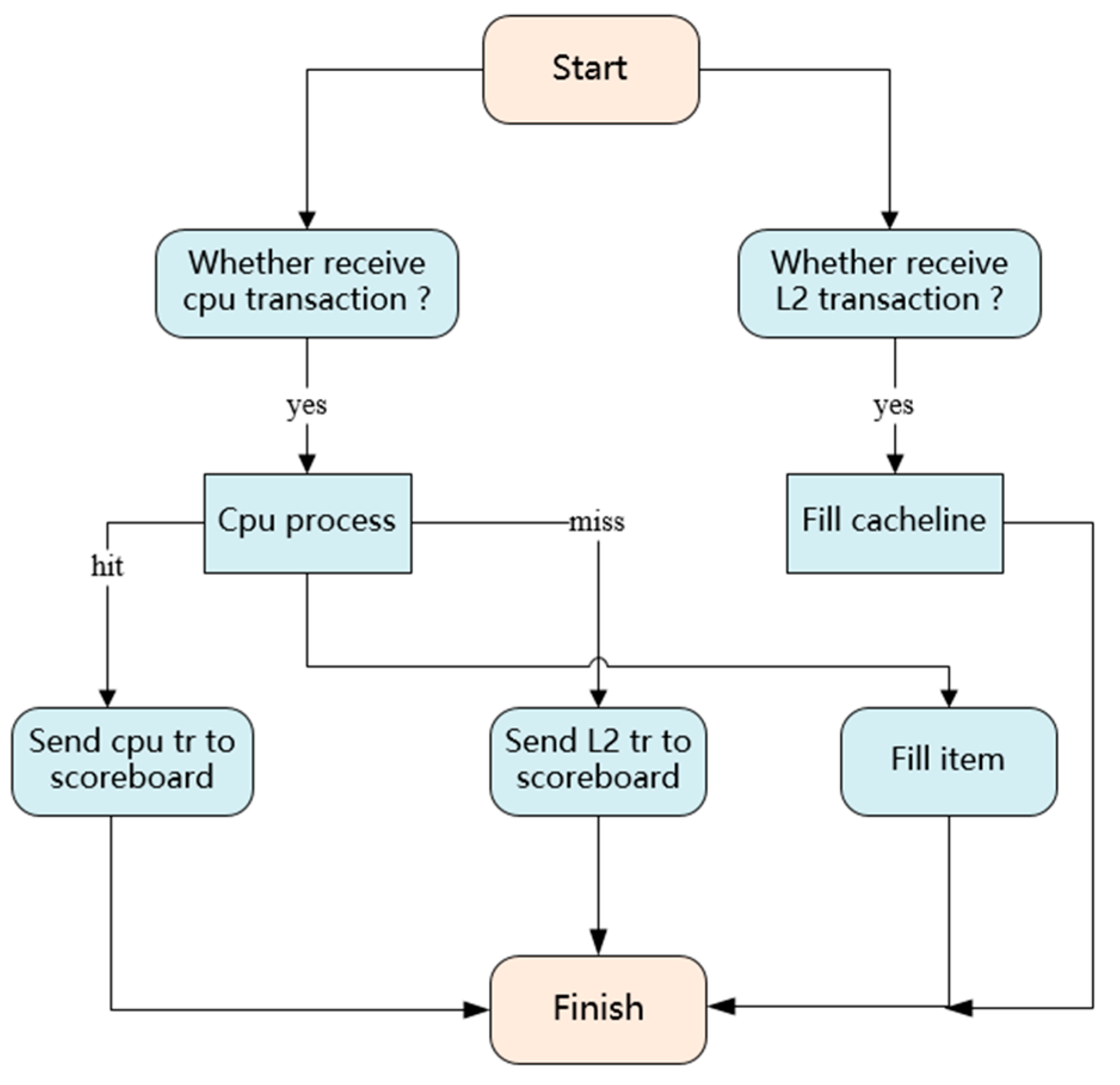
The workflow of the reference model is shown in Figure 5. In the initial state, the model waits to receive transactions from other components. When a transaction is received, it enters the corresponding task for calculation. Depending on the result of the calculation, it either sends the resulting transaction to a different component or enters another task for further processing.
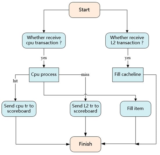
Figure 5.
The workflow of the reference model.
In comparison to the description of the design in register transaction level (RTL) code, the reference model implemented using a high-level language is more abstract and concise, representing a macro-modeling process. For modeling in processor core chips, C++ is commonly used, while matlab finds more utility in the field of communication chips. SystemVerilog supports data types such as arrays and queues, which facilitates details like instruction data storage. In this design, SystemVerilog is employed to implement the reference model, offering the advantage of handling data information at the transaction level rather than the signal level. Transaction-level information is more abstract, resulting in a more concise and efficient operation process. The reference model implemented in this design does not involve delay processing and is a model without time series. The entire process can be summarized in the following steps: receiving the transaction, performing the operation, and sending the result of the operation. The entire process is completed instantaneously and does not require any time.
3.2. Extensibility of the Verification Testbench
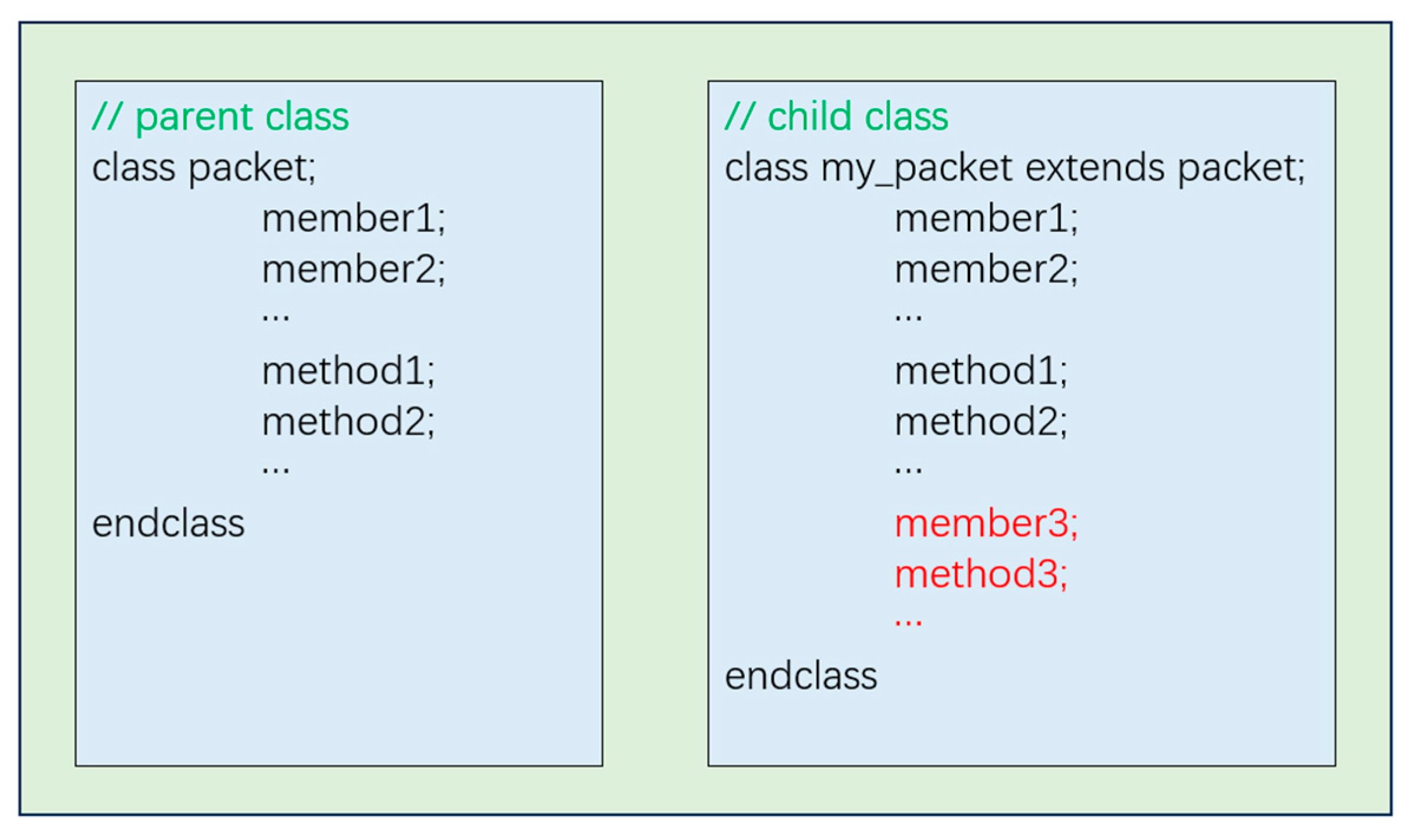
Since the verification testbench proposed in this paper is based on SystemVerilog and UVM, the extensibility of the testbench benefits from the characteristics of both methods. On one hand, SystemVerilog exhibits the traits of an object-oriented language, including encapsulation, inheritance, and polymorphism. Taking inheritance as an example, SystemVerilog allows a child class to inherit all the members and methods of a parent class. A child class not only possess all the elements of a parent class but can also define their own elements. When additional functionality is incorporated into the DUT, a child class can be derived from a parent class, eliminating the need to redefine a new class. As depicted in Figure 6, this process facilitates the extensibility of the verification testbench.
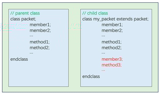
Figure 6.
The inheritance relationship between two classes.
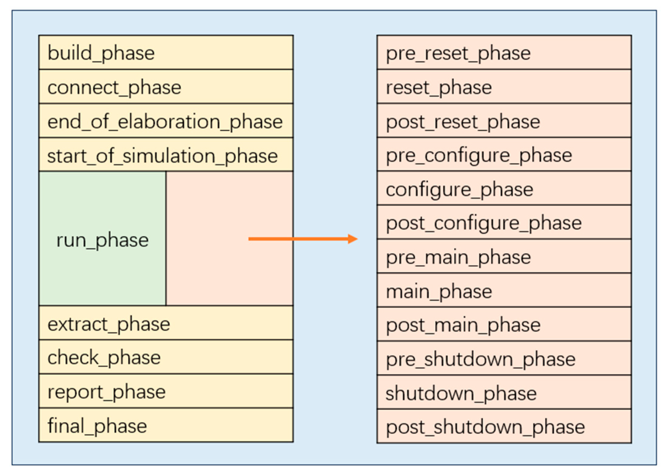
On the other hand, the unique phase mechanism of UVM divides the simulation process into distinct phases, each dedicated to a specific function. For instance, the build_phase oversees the creation of components and variables, while the connect_phase addresses component interconnections. The execution sequence of the UVM phase is illustrated in Figure 7, with each phase being executed from top to bottom. In practice, a typical verification testbench does not utilize all of these phases; rather, it selectively employs specific phases based on its requirements. If the need arises to report important information, a report_phase can be incorporated. Consequently, the utilization of UVM’s phase mechanism further enhances the extensibility of the verification testbench.
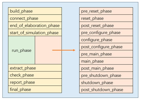
Figure 7.
The execution sequence of the UVM phase.
3.3. Reusability of the Verification Testbench
The verification testbench is designed for an I-Cache controller, which is a module-level design. A module is a part of a system, so the corresponding module-level verification testbench is also a part of a system-level verification testbench. To facilitate, UVM provides transaction-level modeling (TLM) for data interaction among different components. TLM is suitable for the different levels of the verification testbench. The standardization and uniformity of UVM allow for the easy merging and connection of different verification testbenches, which is a significant contribution of UVM towards the reusability of the verification testbench.
Additionally, in the proposed verification testbench, each agent is equipped with a configuration file. This file contains settings for variables and control switches. In certain cases, the usage of the reference model and scoreboard may not be necessary, and they can be deactivated through the configuration file without removing these two components from the verification testbench. This approach not only enhances the flexibility of the verification testbench but also reduces the consumption of EDA tools due to the extensive data processing performed within the reference model. This feature can also be employed in a system-level verification testbench, further enhancing the reusability of the verification testbench.
4. Results and Discussion
Before designing testcases based on the verification methods described in Section 4, we first design incentive sequences that we can use in combination in different testcases to apply different incentives to the DUT. The EDA simulation tool is then used to run all testcases on the verification testbench. This process generates a series of waveform files and simulation log files that can be used to check simulation results. The debugging mechanism of UVM is valuable for checking simulation results. UVM offers various printing macros, including uvm_info, uvm_error, et al., which allow for the setting of importance levels. These macros are typically integrated into testcase code. In case of unexpected outcomes, the macros are printed to the simulation log. By utilizing python scripts to process numerous log files, it becomes possible to identify the testcases that did not pass. Table 2 describes all testcases and provides the corresponding simulation states. All testcases passed simulation, confirming that the corresponding function points were accurately implemented in the design.
Table 2.
Testcase list and simulation states.
4.1. Waveform Analysis
This section analyzes the simulation waveforms of typical working scenarios. Each waveform represents the actual operational state inside the chip, making it an essential basis for assessing the functionality of the module.
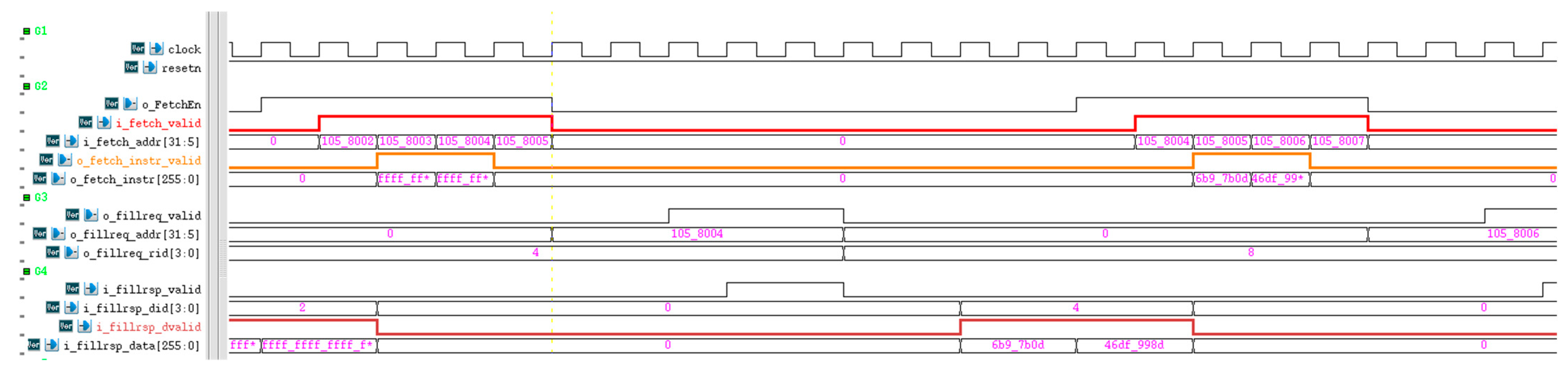
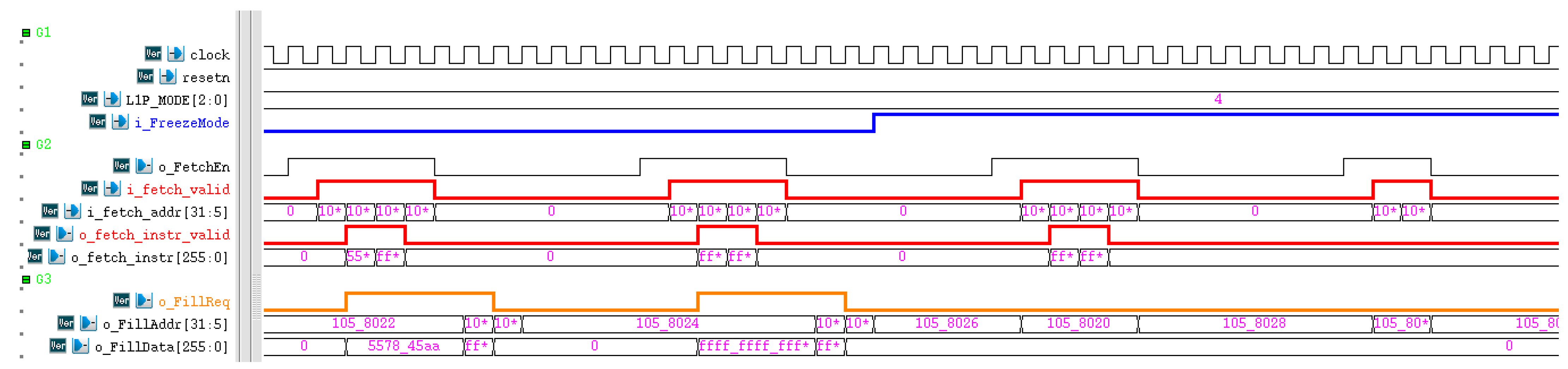
The waveform diagram of sequential fetching is shown in Figure 8. A high level of ‘o_FetchEn’ indicates that fetch operations can be performed at the current time. Meanwhile, ‘i_fetch_valid’ indicates the validity of ‘i_fetch_addr’. ‘o_fetch_instr_valid’ signifies current fetch status, and ‘o_fetch_data’ represents instruction data. When a fetch request is missed, the signal ‘o_fillreq_valid’ becomes active, along with the accompanying request information provided by ‘o_fillreq_addr’ and ‘o_fillreq_rid’. After a certain period of time, the L2 Cache returns data and performs the fetch operation again, resulting in a hit. The situation is similar for branch-fetching instructions, except that the offset address is determined during the instruction-fetch stage.
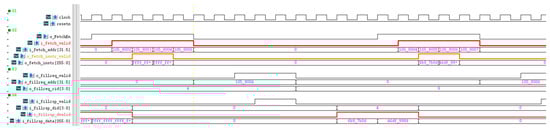
Figure 8.
Waveform diagram of sequential fetch instruction.
If freeze mode is disabled, the data returned from the L2 Cache will be stored in the storage unit when a miss occurs. The ‘o_FillReq’ signal indicates whether the data should be filled. When freeze mode is enabled, data padding is not performed. A miss occurred when the fetch instruction was executed again, which also confirmed that the previous data were not filled. The waveform of freeze mode is shown in Figure 9.
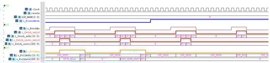
Figure 9.
Waveform diagram of freeze mode.
4.2. Coverage Analysis
By utilizing python scripts, we can automate the execution of testcases and specify the number of runs for each case. It is possible to set up a significant number of runs for random testcases. Out of a total of 4400 testcase simulations, all passed without errors. Upon completion of all simulations, the Verdi tool can be employed to view coverage. Coverage assessment can be categorized into code coverage, functional coverage, and assertion coverage to evaluate the verification progress from different perspectives.
- Code coverage
Code coverage is automatically collected by the Verdi tool without the need to add additional code to the verification testbench. The module’s total code coverage is 99.13%, which includes line coverage, flip coverage, branch coverage, and conditional coverage. These measurements assess the execution of the code from different perspectives, as shown in Figure 10. It can be observed that the code achieves nearly complete coverage, with only a small amount of redundant code.
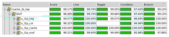
Figure 10.
Results of code coverage.
- Function coverage
To collect function coverage [23,24,25], we need to define function coverage groups and sample coverage groups. As shown in Figure 11, 100% functional coverage indicates that different configuration scenarios are covered during random verification.
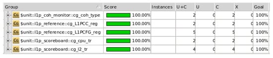
Figure 11.
Results of function coverage.
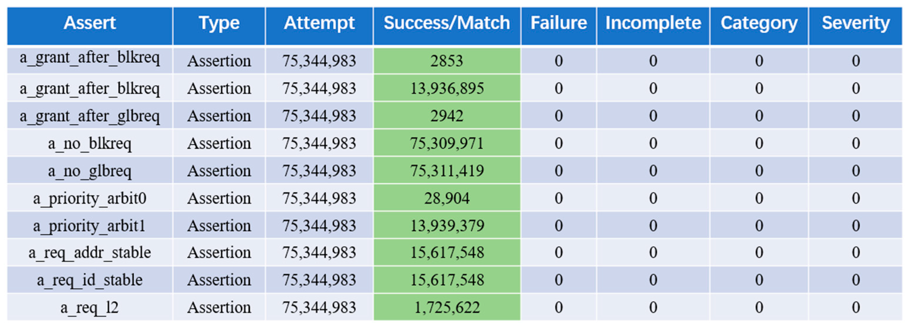
- Assertion coverage
For assertion coverage, the corresponding assertion needs to be defined. Figure 12 is part of an SVA to check the priority relationship of the request signal. As shown in Figure 11, the assertion coverage collected by the verification testbench is 100%, which ensures that no timing errors occur inside the module.
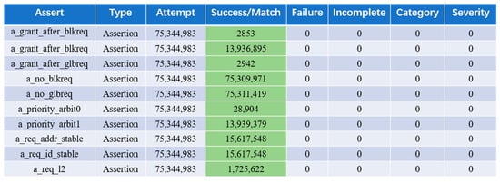
Figure 12.
Results of assertion coverage.
While the simulation results indicate that the code coverage is close to 100%, it does not fully demonstrate the adequacy of the verification process. Code coverage only reflects the current code execution and does not guarantee the proper functioning of the implemented function points or their corresponding functions. For a comprehensive assessment, function coverage is necessary. Additionally, certain special timing relationships, which can be considered as part of the module’s functionality, may not be easily measured by function coverage alone; in such cases, assertion coverage plays a crucial role. These coverages complement each other to ensure the completeness of functional verification. Table 3 provides a description of the comparison among different works. The first work adopted a verification testbench built using traditional Verilog. Although this method is relatively simple and capable of verifying the main functions of the design, it suffers from poor performance and is unsuitable for complex, large-scale digital designs. The second work performed Cache verification based on FPGA. A drawback of this method is its dependence on the specific FPGA device used, resulting in a complicated and non-universal transplantation process. Additionally, this method lacks the ability to observe signal-level information through the simulation waveform, making it less intuitive. The third work designed a UVM verification testbench, which offers good reusability. However, the study lacks a sufficient number of testcases, potentially leading to low code coverage and incomplete verification.
Table 3.
Comparison of several works.
In terms of multiple indicators, our work demonstrates several advantages over others. Firstly, our verification method achieves good verification completeness, not only by running testcases to generate simulation waveforms but also by gathering statistics on different types of coverage. Secondly, our proposed verification testbench exhibits high extensibility, primarily attributed to the inherent advantages of SystemVerilog and the phase mechanism of UVM. Finally, the proposed verification testbench demonstrates a high level of reusability. This is attributed not only to the advantages provided by the TLM communication mechanism of UVM but also to our optimization of the UVM verification testbench. We have implemented a configuration file for each agent, enabling flexible control over individual components. As a result, the proposed testbench becomes easier to reuse in the higher-level verification testbench.
5. Conclusions
This paper proposes a UVM verification testbench for an I-Cache controller. We introduced the composition of the verification testbench and its reference model component. Testcases corresponding to function points were run on the proposed verification testbench and simulation results were obtained. We achieved high coverage by implementing multiple verification methods, which demonstrates the completeness of functional verification. Furthermore, the proposed verification testbench has excellent extensibility and reusability, allowing for its applicability to more advanced verification scenarios without the need for significant modifications. In the future, it is important to consider how to further improve the efficiency of functional verification work, and one potential approach is to leverage machine learning for executing testcases.
Author Contributions
The conceptualization of the research for this project was jointly performed by C.L. and X.X.; C.L. was responsible for software development. B.W. was responsible for review and editing. X.X. and Z.C. were involved in the process of verifying the experimental results. All authors have read and agreed to the published version of the manuscript.
Funding
This work was supported by the China Key System & Integrated Circuit Co., Ltd., China.
Data Availability Statement
Not applicable.
Conflicts of Interest
The authors declare no conflict of interest.
Abbreviations
| UVM | universal verification methodology |
| EDA | electronic design automation |
| SOC | system on chip |
| FPGA | field programmable gate array |
| OVM | open verification methodology |
| SVA | system-Verilog assertion |
| CPU | central processing unit |
| MAF | miss address file |
| MSHR | miss status handling registers |
| OOP | object-oriented programming |
| CDV | coverage-driven verification |
| DUT | design under test |
| RAL | register abstraction layer |
| RTL | register transaction level |
| TLM | transaction level modeling |
References
- Lyu, Y.; Qin, X.; Chen, M.; Mishra, P. Directed Test Generation for Validation of Cache Coherence Protocols. IEEE Trans. Comput.-Aided Des. Integr. Circuits Syst. 2019, 38, 163–176. [Google Scholar] [CrossRef]
- Zhang, R.; Yang, K.; Liu, Z.; Liu, T.; Cai, W.; Milor, L. A Comprehensive Framework for Analysis of Time-Dependent Performance-Reliability Degradation of SRAM Cache Memory. IEEE Trans. Very Large Scale Integr. VLSI Syst. 2021, 29, 857–870. [Google Scholar] [CrossRef]
- Biswal, B.P.; Singh, A.; Singh, B. Cache coherency controller verification IP using SystemVerilog Assertions (SVA) and Universal Verification Methodologies (UVM). In Proceedings of the 2017 11th International Conference on Intelligent Systems and Control (ISCO), Coimbatore, India, 5–6 January 2017; pp. 21–24. [Google Scholar]
- Zhou, S.; Geng, S.; Peng, X.; Zhang, M.; Chu, M.; Li, P.; Lu, H.; Zhu, R. The Design Of UVM Verification Platform Based on Data Comparison. In Proceedings of the 2020 4th International Conference on Electronic Information Technology and Computer Engineering, Xiamen, China, 22–24 October 2021; pp. 1080–1085. [Google Scholar]
- Kaur, G.; Arora, R.; Panchal, S.S. Implementation and Comparison of Direct mapped and 4-way Set Associative mapped Cache Controller in VHDL. In Proceedings of the 2021 8th International Conference on Signal Processing and Integrated Networks (SPIN), Noida, India, 26–27 August 2021; pp. 1018–1023. [Google Scholar]
- Omran, S.S.; Amory, I.A. Implementation of LRU Replacement Policy for Reconfigurable Cache Memory Using FPGA. In Proceedings of the 2018 International Conference on Advanced Science and Engineering (ICOASE), Kurdistan Region, Iraq, 9–11 October 2018; pp. 13–18. [Google Scholar]
- Ali, A.M.; Shalaby, A.; Saif, S.; Taher, M. A UVM-based Verification Approach for MIPI DSI Low-Level Protocol layer. In Proceedings of the 2022 International Conference on Microelectronics (ICM), Casablanca, Morocco, 4–7 December 2022; pp. 74–77. [Google Scholar]
- Wang, J.; Tan, N.; Zhou, Y.; Li, T.; Xia, J. A UVM Verification Platform for RISC-V SoC from Module to System Level. In Proceedings of the 2020 IEEE 5th International Conference on Integrated Circuits and Microsystems (ICICM), Nanjing, China, 23–25 October 2020; pp. 242–246. [Google Scholar]
- Anwar, M.W.; Rashid, M.; Azam, F.; Naeem, A.; Kashif, M.; Butt, W.H. A Unified Model-Based Framework for the Simplified Execution of Static and Dynamic Assertion-Based Verification. IEEE Access 2020, 8, 104407–104431. [Google Scholar] [CrossRef]
- Chen, P.; Yue, J.; Liao, X.; Jin, H. Trade-off between Hit Rate and Hit Latency for Optimizing DRAM Cache. IEEE Trans. Emerg. Top. Comput. 2018, 9, 55–64. [Google Scholar] [CrossRef]
- Choi, H.; Park, S. Learning Future Reference Patterns for Efficient Cache Replacement Decisions. IEEE Access 2022, 10, 25922–25934. [Google Scholar] [CrossRef]
- Jiang, L.; Zhang, X. Cache Replacement Strategy with Limited Service Capacity in Heterogeneous Networks. IEEE Access 2020, 8, 25509–25520. [Google Scholar] [CrossRef]
- Xiong, W.; Katzenbeisser, S.; Szefer, J. Leaking Information Through Cache LRU States in Commercial Processors and Secure Caches. IEEE Trans. Comput. 2021, 70, 511–523. [Google Scholar] [CrossRef]
- Desalphine, V.; Dashora, S.; Mali, L.; Suhas, K.; Raveendran, A.; Selvakumar, D. Novel Method for Verification and Performance Evaluation of a Non-Blocking Level-1 Instruction Cache designed for Out-of-Order RISC-V Superscaler Processor on FPGA. In Proceedings of the 2020 24th International Symposium on VLSI Design and Test (VDAT), Bhubaneswar, India, 23–25 July 2020; pp. 1–4. [Google Scholar]
- Kanhaiya, P.S.; Lau, C.; Hills, G.; Bishop, M.D.; Shulaker, M.M. Carbon Nanotube-Based CMOS SRAM: 1 kbit 6T SRAM Arrays and 10T SRAM Cells. IEEE Trans. Electron Devices 2019, 66, 5375–5380. [Google Scholar] [CrossRef]
- Ling, M.; Lin, Q.; Tan, K.; Shao, T.; Shen, S.; Yang, J. A Design of Timing Speculation SRAM-Based L1 Caches With PVT Autotracking under Near-Threshold Voltages. IEEE Trans. Very Large Scale Integr. VLSI Syst. 2021, 29, 2197–2209. [Google Scholar] [CrossRef]
- Hussien, A.; Mohamed, S.; Soliman, M.; Mostafa, H.; Salah, K.; Dessouky, M.; Mostafa, H. Development of a Generic and a Reconfigurable UVM-Based Verification Environment for SoC Buses. In Proceedings of the 2019 31st International Conference on Microelectronics (ICM), Cairo, Egypt, 15–18 December 2019; pp. 195–198. [Google Scholar]
- Massoud, E.; AbdelSalam, M.; Safar, M.; Watheq El-Kharashi, M. A Reusable UVM-SystemC Verification Environment for Simulation, Hardware Emulation, and FPGA Prototyping: Case Studies. In Proceedings of the 2022 International Conference on Microelectronics (ICM), Casablanca, Morocco, 4–7 December 2022; pp. 38–41. [Google Scholar]
- Wang, J.; Liu, J.; Wang, D.; Zhang, S.; Fan, X. MemUnison: A Racetrack-ReRAM-Combined Pipeline Architecture for Energy-Efficient in-Memory CNNs. IEEE Trans. Comput. 2022, 71, 3281–3294. [Google Scholar] [CrossRef]
- El-Ashry, S.; Adel, A. Efficient Methodology of Sampling UVM RAL during Simulation for SoC Functional Coverage. In Proceedings of the 2018 19th International Workshop on Microprocessor and SOC Test and Verification (MTV), Austin, TX, USA, 9–10 December 2018; pp. 61–66. [Google Scholar]
- Na, J.; Yang, J.; Gao, G. Reinforcing Transient Response of Adaptive Control Systems Using Modified Command and Reference Model. IEEE Trans. Aerosp. Electron. Syst. 2019, 56, 2005–2017. [Google Scholar] [CrossRef]
- Hosny, S. A Unified UVM Methodology For MPSoC Hardware/Software Functional Verification. In Proceedings of the 2022 11th International Conference on Modern Circuits and Systems Technologies (MOCAST), Bremen, Germany, 8–10 June 2022; pp. 1–5. [Google Scholar]
- Adel, A.; Saad, D.; El Mawgoed, M.A.; Sharshar, M.; Ahmed, Z.; Ibrahim, H.; Mostafa, H. Implementation and Functional Verification of RISC-V Core for Secure IoT Applications. In Proceedings of the 2021 International Conference on Microelectronics (ICM), Cairo, Egypt, 19–22 December 2021; pp. 254–257. [Google Scholar]
- Harshitha, N.B.; Kumar, Y.G.P.; Kurian, M.Z. An Introduction to Universal Verification Methodology for the digital design of Integrated circuits (IC’s): A Review. In Proceedings of the 2021 International Conference on Artificial Intelligence and Smart Systems (ICAIS), Tamil Nadu, India, 25–27 March 2021; pp. 1710–1713. [Google Scholar]
- Xu, C.; Ni, W.; Song, Y. UVM-based Functional Coverage Driven AXI4-Stream Verification. In Proceedings of the 2019 IEEE 13th International Conference on ASIC (ASICON), Chongqing, China, 29 October–1 November 2019; pp. 1–4. [Google Scholar]
- Liang, K.; Wu, J.; Ren, H.; Zhang, Z.; Tan, B. Design and Implementation of DSP Cache. In Proceedings of the 2021 IEEE 21st International Conference on Communication Technology (ICCT), Virtual, Montreal, QC, Canada, 14–23 June 2021; pp. 993–997. [Google Scholar]
- Tiejun, L.; Jianmin, Z.; Sikun, L. An FPGA-based Random Functional Verification Method for Cache. In Proceedings of the 2013 IEEE Eighth International Conference on Networking, Architecture and Storage, Xi’an, China, 17–19 July 2013; pp. 277–281. [Google Scholar]
- El-Ashry, S.; Khamis, M.; Ibrahim, H.; Shalaby, A.; Abdelsalam, M.; El-Kharashi, M.W. On Error Injection for NoC Platforms: A UVM-Based Generic Verification Environment. IEEE Trans. Comput.-Aided Des. Integr. Circuits Syst. 2020, 39, 1137–1150. [Google Scholar] [CrossRef]


Disclaimer/Publisher’s Note: The statements, opinions and data contained in all publications are solely those of the individual author(s) and contributor(s) and not of MDPI and/or the editor(s). MDPI and/or the editor(s) disclaim responsibility for any injury to people or property resulting from any ideas, methods, instructions or products referred to in the content. |
© 2023 by the authors. Licensee MDPI, Basel, Switzerland. This article is an open access article distributed under the terms and conditions of the Creative Commons Attribution (CC BY) license (https://creativecommons.org/licenses/by/4.0/).