Article

Indirect Matrix Converter Hardware-in-the-Loop Semi-Physical Simulation Based on Latency-Free Decoupling

1
School of Electrical Engineering and Automation, Xiamen University of Technology, Xiamen 361024, China
2
Xiamen Key Laboratory of Frontier Electric Power Equipment and Intelligent Control, Xiamen 361024, China
3
Nuclear Power Operations Research Institute (NPRI), Shanghai 200131, China
*
Author to whom correspondence should be addressed.
Electronics 2023, 12(23), 4802; https://doi.org/10.3390/electronics12234802
Submission received: 7 September 2023 / Revised: 18 November 2023 / Accepted: 21 November 2023 / Published: 27 November 2023

Abstract

:
In the process of hardware-in-the-loop simulations (HILs) of indirect matrix converters (IMCs), solving the mathematical models of complex multiswitching converter topologies has become a major problem. The conventional approach is to split the complex mathematical model into multiple serial subsystems; however, this inevitably produces delays in the simulation steps between different subsystems, leading to numerical oscillations. In this paper, the method of latency-free decoupling is adopted, which has no time-step delay between different subsystems, making each subsystem a parallel operation. This can improve the numerical stability of the simulations and can effectively reduce the step size of the real-time simulation and alleviate the problem of real-time simulation resource consumption. In this paper, we discuss in detail the modeling process of IMC hardware-in-the-loop simulations with Finite Control Set Model Predictive Control (FCS-MPC), and experimentally validate our method using the Speedgoat test platform, resulting in a simulation step size of less than 200 ns. The simulation results are compared with the results of Matlab’s Simpower power system, which allows us to evaluate the accuracy of our model.

1. Introduction

With the development of power electronics and computer control, research on matrix converters (MCs) has been receiving increasing attention. MCs are advanced topology power converters, which have the advantages of a simple topology, no intermediate energy storage links, low harmonic pollution to the grid, a sinusoidal input current and output voltage, an input power factor of 1, an adjustable output voltage amplitude and frequency, a bi-directional energy flow, etc. [1]. It has been proposed that MCs should be used in motors by adopting an indirect control technique, which reduces the switching losses, and should be applied in hospital pumping or vehicle applications [2].
IMCs not only have these same advantages, but they also overcome the disadvantages of conventional MCs, such as the complex control strategy and multiple switches, making them a new type of MC with great development potential. For example, the authors of [3] propose a new type of IMC with an open rectifier stage— the first of its kind—creating a new class by replacing the four active control switches of the rectifier stage with four diodes, which reduces the cost and improves the efficiency. For the control algorithm of IMCs, in [4], FCS-MPC for IMC control is proposed to realize a model with a controllable input power, a controllable load power and a fixed switch output waveform. In [5], several mainstream three-phase AC-AC converters were reviewed and compared, and the implementation of space vector modulation (SVM) and the corresponding switching mode generator was introduced. The authors of [6] propose the realization of FCS-MPC through virtual vector modulation, which can effectively reduce the error of current control methods and was proven to improve the steady-state control performance of IMCs.
In the control system development phase, simulation testing techniques that allow testing without first building the physical system are called HILs. However, with the rapid development of power electronics technologies, the converter’s switching frequency has become increasingly demanding. For example, the control frequency of IMCs is generally more than 20 kHz; in order to more accurately simulate an actual situation, the model’s simulation step size generally needs to be 100 times more than the control frequency, which means that a real-time IMC simulation requires a very small simulation step size to meet the system requirements. Therefore, the real-time simulation modeling of IMCs is challenging.
Usually, this can be solved by changing the hardware or improving the simulation modeling method; for example, in [7], a method of determining matrix equations based on a modified node voltage analysis is proposed to cope with high-frequency switching power electronic converter modeling and real-time simulations. HIL model construction is realized using a dual active bridge converter as an example. The authors of [8] proposed a method with which to improve the circuit models of field programmable gate arrays (FPGAs), eliminating the problem due to synchronization errors between the simulation time network and the control platform and enhancing its scalability. As for device-level developments, ref. [9] proposes a real-time, high-voltage, high-current silicon carbide metal–oxide semiconductor field-effect transistor half-bridge power module modeling method using FPGAs, which employs Eulerian discretization to discretize the state-drain current, gate-source voltage and drain-source voltage of the device. The model was applied to medium- and high-voltage DC-DC dual active bridge converters, achieving time efficiency and producing current values under various voltage and current levels for on and off transients. The model can be generalized to other SiC-based power electronics systems. A methodology for the alternative compensated voltage source interfaces required for the real-time simulation of power systems is presented in ref. [10]. Application of a generalized equivalent model to a hybrid multilevel converter is presented in ref. [11], where the combination of CPUs and FPGAs effectively improved the model accuracy and computational efficiency. In ref. [12], a generalized equivalent model that can be applied to wind power systems and modular multi-level converters (MMCs) is proposed; in addition, ref. [13] proposes a voltage-balancing method for MMCs, which was verified as being superior to the conventional method for HILs. In [14], on the other hand, an HILS system was used to verify the feasibility of a supercapacitor variface to protect equipment connected to a distributed power supply in the case of a low-voltage overcurrent with a power compensator.
In real-time simulations of a circuit model, the selection of an appropriate decoupling method determines the model’s minimum delay path for real-time simulations, and the minimum delay path determines the minimum step size that can be achieved in the simulation. The current mainstream decoupling method, the delay insertion decoupling method, is usually used. In [15], the delay insertion method (LIM) is used for real-time simulations of power electronic systems with high switching frequencies and common power topologies, with a description of how to create an LIM three-phase DC/AC converter model to prove its feasibility. In ref. [16], a new parallel simulation method is proposed, which does not include a time step delay over the entire system division process. By dividing the system into a two-step prediction and control simulation, the overall system stability is improved. The method was verified using the RTLAB simulator and the method’s effectiveness was proven using the results of the Simpower system in Matlab for comparison. The authors of ref. [17], using a solid-state transformer as an example, proposed a hybrid accompanying circuit modeling method and electromagnetic transient program method combined with the traditional EMTP computational tasks. The parallelization of the FPGA’s hardware structure was taken full advantage of, a compact EMTP algorithm was designed and the same type of offline playback was used to verify the model’s accuracy. Ref. [18] proposes a new approach to circuit decoupling and segmentation, where each state variable is discretized in a different way, combining implicit and explicit methods to decouple the system without the need for artificial delay compensation. This method can be applied in the commercial market. Ref. [19] proposes a multi-rate delay insertion method for fast transient simulations which can be used in large-scale interconnected planar networks and can effectively reduce the computational cost.
In contrast, this paper focuses on the real-time simulation of mainstream traditional IMC circuits. The non-delay decoupling method is introduced to improve the accuracy of the model, reduce the simulation time steps and improve the FPGA’s resource consumption problem. The traditional IMC FCS-MPC method is introduced and, finally, the HILs IMC circuit model is realized. The Simpower system simulation results in Matlab and the FPGA’s resource consumption are compared to verify the accuracy and effectiveness of the model.
This paper is organized as follows. In Section 2, the mathematical IMC circuit topology model and the application of the FCS-MPC algorithm are introduced in detail. Section 3 details the circuit division method used by LFD and applies it to IMC circuits. Then, for benchmarking purposes, in Section 4, a real-time simulation of our model in Speedgoat is detailed and it is compared to the SPS model. Finally, the paper is summarized in Section 5.

2. Circuit Topology of IMCs

2.1. IMC Mathematical Model

An IMC is mainly composed of a filter circuit, a rectifier stage and an inverter stage; the intermediate DC link does not require additional energy storage capacitor components. Figure 1 shows a typical IMC circuit; the operation principle is that the three-phase AC voltage is first converted to DC by the rectifier stage and then converted to three-phase AC again in the inverter stage. The IMC control of both the output voltage and input current can effectively be decoupled from each other, allowing the input voltage to be generated independently of the input. Regardless of the input voltage value, it can be used to control the phase of the input current.
When the switch is modeled using the ideal switch model, the signals on the rectifier side and inverter side are S r i and S i i . In the circuit topology shown in Figure 1, a mathematical IMC model regarding the current–voltage input–output relationship can be derived, where the switching signal takes a value of 0 or 1 and the DC bus voltage U D C is as follows:
U D C = T r u i i
where the input voltage u i i = [ u a i u b i u c i ] T and T r is the instantaneous transmission matrix at the input.
T r = [ S r 1 S r 4 S r 3 S r 6 S r 5 S r 2 ]
The input current i i i = [ i a i i b i i c i ] T is equal to the DC bus current I d c multiplied by the instantaneous transfer matrix transpose T r T at the input:
i i i = T r T I D C
Meanwhile, the DC bus current I d c is equal to the instantaneous transfer matrix at the output multiplied by the output current i i o :
I D C = T i i i o
where i i o = [ i a o i b o i c o ] T . The instantaneous transmission matrix T i at the output is as follows:
T i = [ S i 1 S i 2 S i 3 ]
The output three-phase voltage u i o = [ u a o u b o u c o ] T is equal to the instantaneous transmission matrix at the output multiplied by the instantaneous transmission matrix at the output of the DC bus voltage U D C :
u i o = T i T U D C
Based on the output three-phase load, it can be concluded that the three-phase load currents add up to zero:
i a o + i b o + i c o = 0
The circuit parameters of the IMC are shown in Table 1.
The IMC input–output relationship can be observed by looking at the entire circuit topology. The energy has a bi-directional flow, where the input voltage determines the output current and the load current on the load side feeds back to determine the input current; therefore, the circuit decoupling process requires special treatment.

2.2. IMC Control

The current control algorithms applied to IMC controllers are mainly FCS-MPC and SVPWM modulation; the FCS-MPC method has been validated in [4]. The aim is to obtain a close reference current, i i o * , and to minimize the instantaneous input power. The control steps are shown in Figure 2 and the main control steps are determined by the following three steps:
(1)
First, define the reference current i i o * and set the input reference power q * = 0 . It is necessary to measure the input voltage u i i , the input current i i s , the rectifier-side input voltage u i i and the output current i i o .
(2)
Predict the next occurrence of u i o and i i o from the switching state and measured values.
(3)
Finally, the predicted values are used to calculate the cost function k. The predicted values that minimize the cost are selected and the switching state is output. Since the predictive controller is formulated in discrete time, it is necessary to derive a discrete time model of the load converter system. The predictive variables at the input side are as follows:
[ u i i ( k + 1 ) i i s ( k + 1 ) ] = α [ u i i ( k ) i i s ( k ) ] + β [ u i s ( k ) i i i ( k ) ]
where α e A T S and β A 1 ( α I 2 x 2 ) B , with
A = [ 0 1 / C f 1 / L f R f / L f ] , B = [ 0 1 / C f 1 / L f 0 ]
The value of U D C at the k+1-th instant is obtained via Equation (10).
U D C ( k + 1 ) = T r ( k + 1 ) u i i ( k )
The predicted load current can be obtained using the forward Euler approximation:
i i o ( k + 1 ) = d 1 ( u i o ( k ) + d 2 ( i i o ( k ) )
where d 1 = T s / L L and d 2 = 1 ( R L / L L ) T s are constants dependent on the load parameters and the sampling time T s . The output current, io, is measured at the k-th instant and the value of vo at the k-th instant is given according to Equations (6) and (10).
On the output side, the error between the load currents and their respective references is given as follows:
Δ i i o ( k + 1 ) = ( i a o * ( k ) i a o ( k ) ) 2 + ( i b o * ( k ) i b o ( k ) ) 2 + ( i c o * ( k ) i c o ( k ) ) 2
For this, the reference Q i n = 0 is used. The function that determines the minimization of the instantaneous reactive power is
Δ Q i n ( k + 1 ) = v s α ( k ) i s β ( k ) + i s α ( k ) v s ( k ) β
where the current i s α ( k ) and i s β ( k ) are two-phase current static coordinate system components, and voltage v s α ( k ) and v s ( k ) β are two-phase static coordinate system components.
Since there are two cost functions, the combination requires a cost weight λ to determine the impact component of the two cost functions:
k = Δ i i o ( k + 1 ) + λ Δ Q i n ( k + 1 )
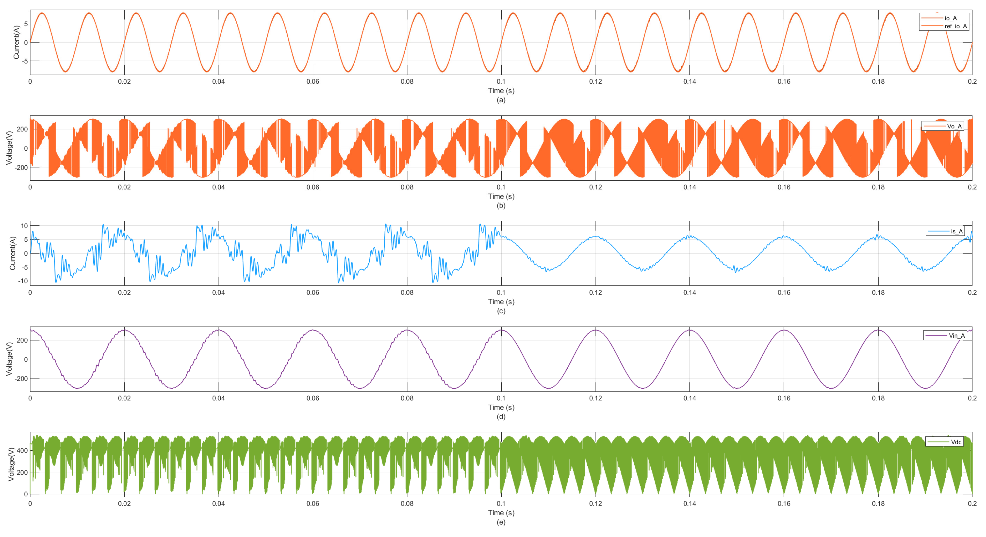
Based on this, the IMC is modeled using a power device, namely the Simulink power system (SPS) library, in Matlab R2022b Simulink. The offline simulation results are shown in Figure 3. In order to evaluate the results of instantaneous reactive power minimization, the system does not consider reactive power tracking before t = 0.1 s, i.e., the cost weight of the reactive power is 0, and the weighting is equal to 1 after t = 0.1 s. Figure 3a,b shows the output current, i o A , and output voltage, u o A , of phase A; Figure 3c,d shows the input current, i A s , and input voltage, u A i , of phase A; and Figure 3e shows the DC bus voltage. Only the output current is tracked; thus, the reactive power is in an oscillating state, and after 0.1 s, the instantaneous reactive power is almost zero.

3. Decoupled Modeling Analysis

3.1. Latency-Free Decoupling Approach

For conventional decoupling, the inductance and capacitance are transformed into state-space equations, which are solved using forward Euler or backward Euler approximations, and various subsystems are established with sequential execution relationships between the systems. Conversely, latency-free decoupling involves splitting the systems into subsystems that are executed in parallel on the basis of the forward Euler approximation to improve the simulation speed.
The use of latency-free decoupling with multiple subsystems, where each subsystem does not have a beat delay and does not lose precision, can effectively reduce the matrix dimension and reduce the computation amount. Additionally, as shown in Figure 4a, after including latency-free decoupling in the operation process, the two subsystems are used in parallel operation and the system waiting time is determined by the two subsystems in the single largest subsystem simulation time step; meanwhile, for the conventional delayed decoupling method shown in Figure 4b, the subsystem I I execution can only be started after the completion of subsystem I execution. This leads to the overall system simulation time being equal to the sum of the two subsystems’ simulation time steps. It can clearly be seen that latency-free decoupling can effectively reduce the simulation time steps.
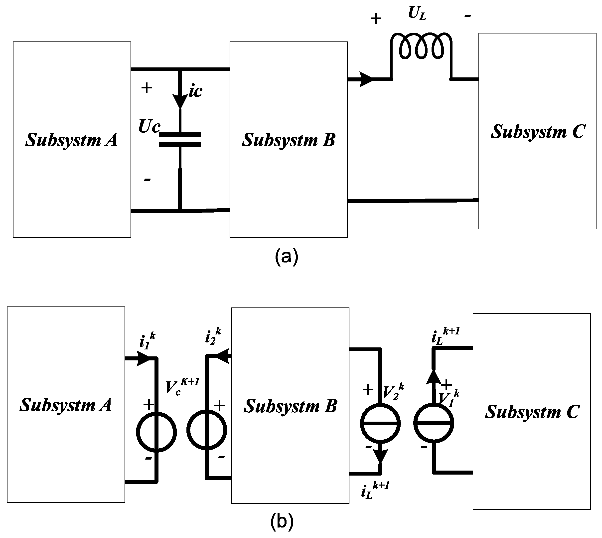
As shown in Figure 5—the latency-free decoupling schematic—assuming that the entire large system has parallel capacitance and series inductance as a result of the division into three subsystems, where Subsystems A and B are connected through the capacitance between Subsystems B and C which are connected through inductance, at this time, the relationship between the voltage and the current at the two ends of the capacitance and the forward Eulerian discretization of the formula are described as follows:
C d V C d t = i 1 + i 2
V C k + 1 = V C k + h C ( i 1 k + i 2 k )
in which k + 1 represents the current moment of the simulation, k indicates the previous simulation moment, h represents the simulation step size, i 1 k is the output current of the last moment of Subsystem A and i 2 k is the output current of the last moment of Subsystem B.Similarly, by the forward Eulerian decoupling of the inductor, one can derive the voltage∓current relationship for splitting its two terminals at the inductor, which is equivalent to the current source at the inductor. This discretization equation is as follows:
L d i L d t = V 2 V 3
i L k + 1 = i L k + h L ( V 2 k V 3 k )
In this case, for each subsystem, only the variables V C k + 1 and i L k + 1 need to be updated; the updated variables are obtained from the respective last simulation moment K, thus realizing their non-interference at moment k + 1 . Not all inductors and capacitors are suitable for latency-free decoupling, and the remaining inductors and capacitors need to be processed in order to reduce the computation amount. In addition to the capacitance and inductance of latency-free decoupling, the remaining inductance and capacitance can be replaced by a linearized model and then introduced in the differential form of the equation of state.
i c k = C V c k V C k 1 h
where h is the time interval, simplified as follows:
i c k = G C V c k + i s k 1
G C = C h
The same can be done for the inductor:
V L k = L i L k i L k 1 h
which results in the simplified
i L k = G L V L k + i s k 1
G L = h L c
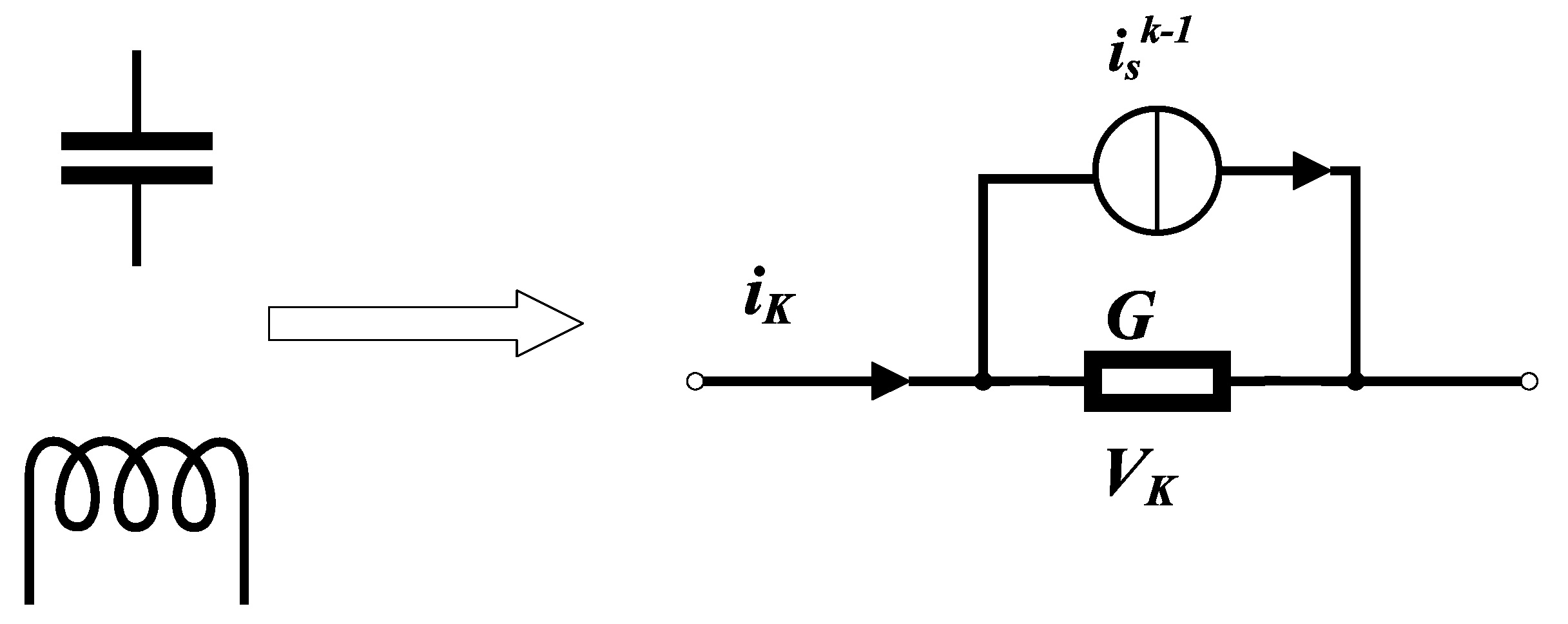
The equivalent circuit is shown in Figure 6, where the G C G L value remains constant across transient calculations and only the equivalent current source i s k 1 changes. For the IMC circuit, all the remaining capacitive inductance is replaced by the equivalent circuit in Figure 6, where the current source is in parallel with the conductance G, constituting a purely resistive network.

3.2. Switch Status Update

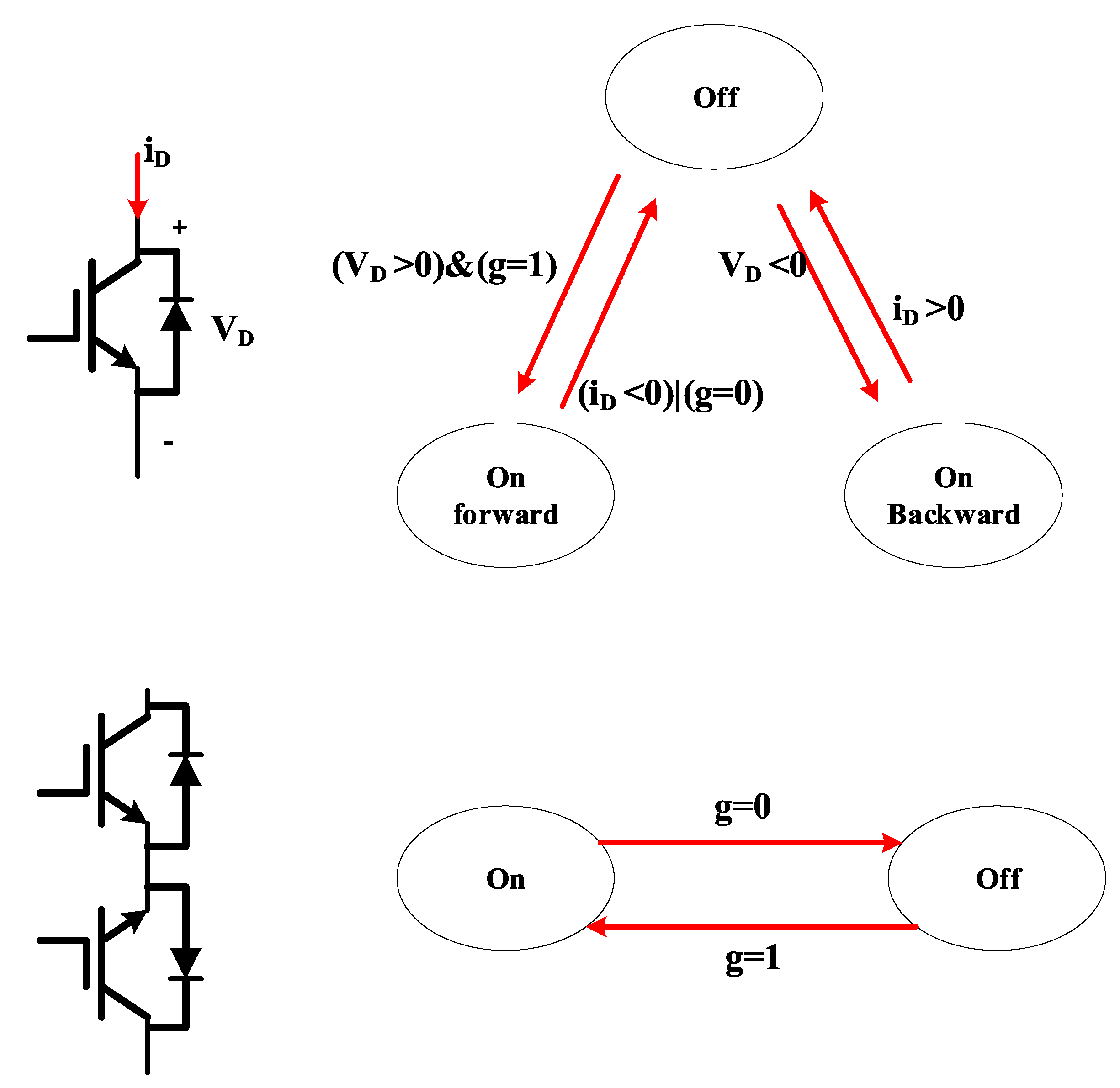
In the modeling process, the update rule of the switch state directly determines whether the switch state is accurate or not. Taking an IMC as an example, in this paper, specific judgment conditions are presented for the switch state of the two switch types, alongside an IGBT with an anti-parallel diode and a double-series anti-parallel diode IGBT, as shown in Figure 7. As both are active switching devices, the switching state update should be determined by the voltage v at the terminals and the current i flowing through it, in addition to the extra external control signal g. Therefore, for an IGBT with an anti-parallel diode:
S k + 1 = S k ( i k > 0 ) + S ¯ k ( v k < 0 ) + g k + 1
As for the double series anti-parallel diode IGBT, since it is determined by two control signals g, without considering the dead time, the two control signals can be considered the same due to the opposite direction of the series connection of the two switches. This results in the two having the same signal, and the values of the current i k and voltage v k can be considered as being the same. Therefore, it can be assumed that the switching state update is equal to the external control signal, g, as follows:
S k + 1 = g k + 1

3.3. Modeling Analysis Steps

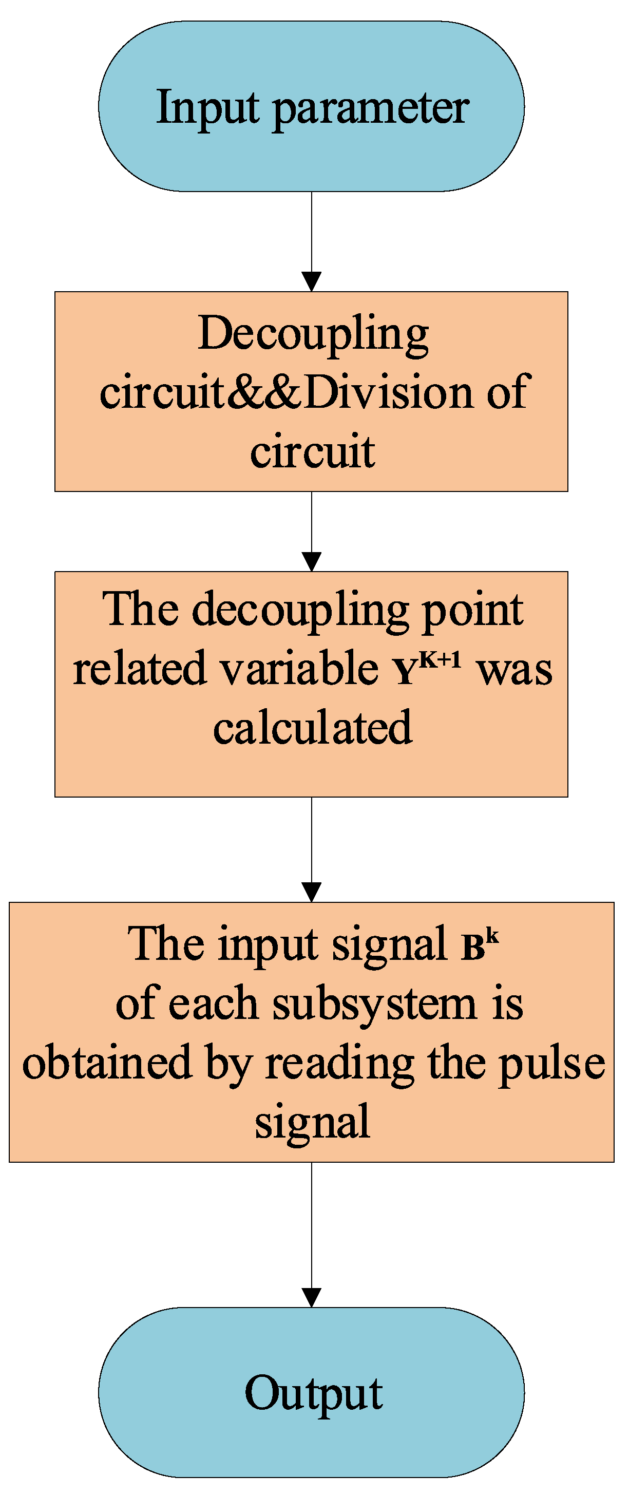
The steps of the modeling approach incorporating latency-free decoupling are shown in Figure 8 and described as follows:
(1)
The circuit is first split using latency-free decoupling at the selected shunt inductor and series capacitor after forward Eulerian discretization to obtain the correlation variables Y k + 1 , i.e., the capacitance voltage and the inductance current, at the decoupling.
(2)
The passive elements in the remaining circuit are then discretized and equated to a Norton-equivalent circuit, and then the state space equations are written according to Kirchhoff’s voltage–current law.
(3)
Then, according to the switch update rule, the switch update state is determined via the control signal, switch current, and voltage, and combined with the correlation variable Y k + 1 in step (1). Each subsystem input B k is then reconstructed.
(4)
The state equations for each subsystem are computed in parallel, and the next step-length vector X k + 1 is output.

3.4. IMC Decoupled Modeling

For a three-phase symmetrical circuit, in the process of latency-free decoupling, regardless of whether it is inductive decoupling or capacitive decoupling, decoupling is not a general one-port network and it is necessary to introduce a neutral point n for decoupling. Figure 9 shows the various subsystem parts of the IMC circuit after latency-free decoupling, which can be classified as a power system, a rectifier system, an inverter system, and a load system. The decoupling between the power system and the rectifier–inverter system at the three-phase filter capacitor requires the introduction of a neutral point N c , as shown in Figure 9a,b. According to Kirchhoff’s voltage and current theorems, the neutral point N c potential can be derived as follows:
U N C = u A + R f × i a s + L f d i a s d t + u a i
U N C = u B + R f × i b s + L f d i b s d t + u b i
U N C = u C + R f × i c s + L f d i c s d t + u c i
i a s + i b s + i c s = 0
At this point, it can be concluded from the symmetry of the three symmetrical power supplies that the voltages add up to 0. If
u A + u B + u C = 0
and u i i = C d i i i d t , it follows that U N C = 0 .
Similarly, as shown in Figure 9c,d, the three-phase load in the three-phase symmetrical inductance decoupling, according to Kirchhoff’s voltage–current theorem, can be derived from the load end decoupling neutral point, N L , potential.
U N L = 1 3 ( u a N + u b N + u c N )
The nodal voltage equation for system a can be written as follows:
u i ( k + 1 ) i i s ( k + 1 ) R f ( i i s ( k + 1 ) + i i a ( k + 1 ) ) / G = u i i ( k + 1 )
Equation (26) can be derived from the latency-free decoupling equation:
u i i ( k + 1 ) = u i i k + h / C ( i i s k + i i i k )
It can be shown that the only variable that needs to be updated is u i ( k + 1 ) , and the rest of the variables are available from the previous step. Similarly, for systems B and C, only the switching state variables need to be updated, and the rest of the variables can be obtained from the previous step. For the loaded system, inductive decoupling is used here and can be written as follows:
i i o ( k + 1 ) = i i o k + h / L ( u i o k u L o k )
u L o ( k + 1 ) = U N L ( k + 1 ) + i i o k × R L
According to the above equation, it can be seen that the various subsystems do not interfere with each other, and the inputs of each system can be realized at the same time to realize parallel operation. Thus, the latency-free decoupling model of IMCs has been established.

4. Experiments

4.1. Experimental Environment

Experiments were conducted on the official Speedgoat real-time simulator from Mathworks, model IO324, with an Intel Core i7 4.2 GHz 4 core CPU supporting multiple I/O interfaces, and a Xilinx Artix-7 FPGA board.
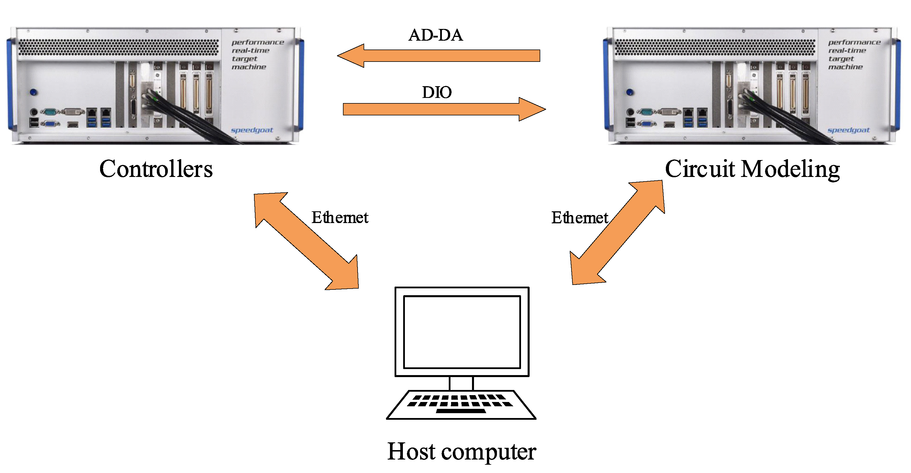
The overall simulation design is shown in Figure 10, showing that two Speedgoat real-time simulators are used for real-time simulations, one of which runs the FCS-MPC control algorithm as a controller in its CPU environment, while the other runs the simulation circuit as a controlled object. In this simulation, the real-time simulator exchanges information through an Ethernet connection, and when running in real time, the controlled circuit sends the collected current and voltage information to the controller via analogue. The controller performs the control calculation in real time after receiving the voltage and current signals, and sends the result to the controlled circuit via digital signals.
The specific environment of the experiment is shown in Figure 11, where (1) is the host computer for operation and control, (2) is the oscilloscope which can observe the output waveforms in real time, (3) is the Speedgoat 1 simulator, which carries out real-time simulations of the circuit model in the internal FPGA and (4) is the Speedgoat 2 simulator, which runs the control algorithm in the CPU environment. The information is extracted through the analogue and digital boards ((5) and (6)).

4.2. Real-Time Simulation Results

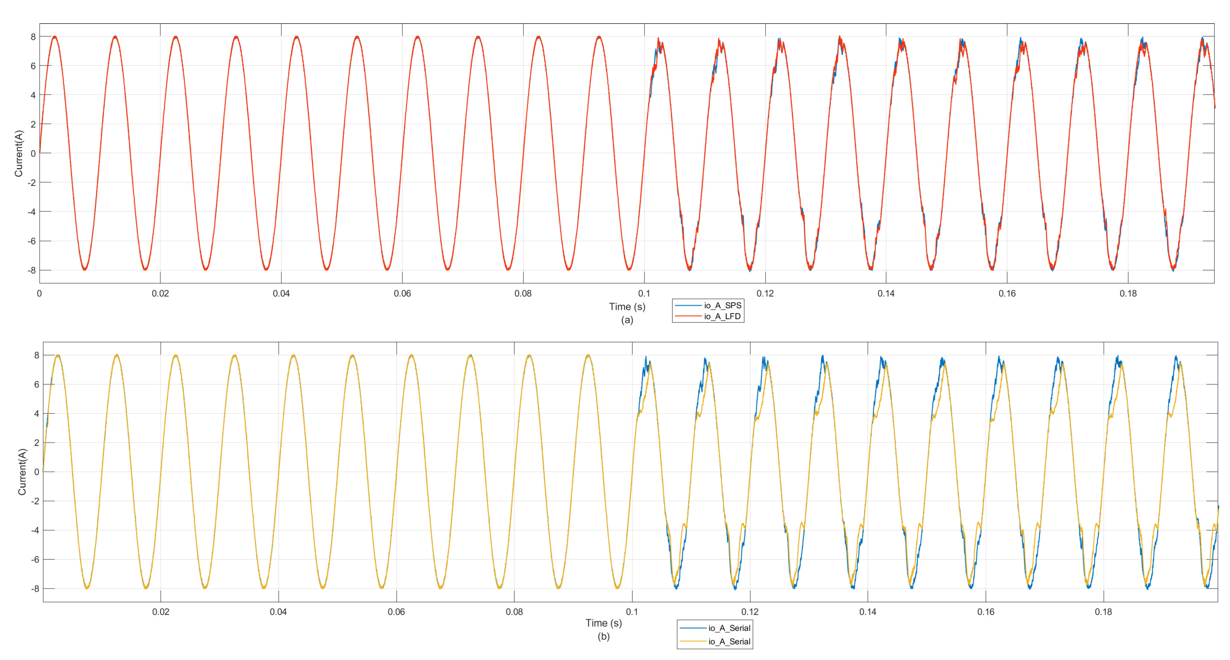
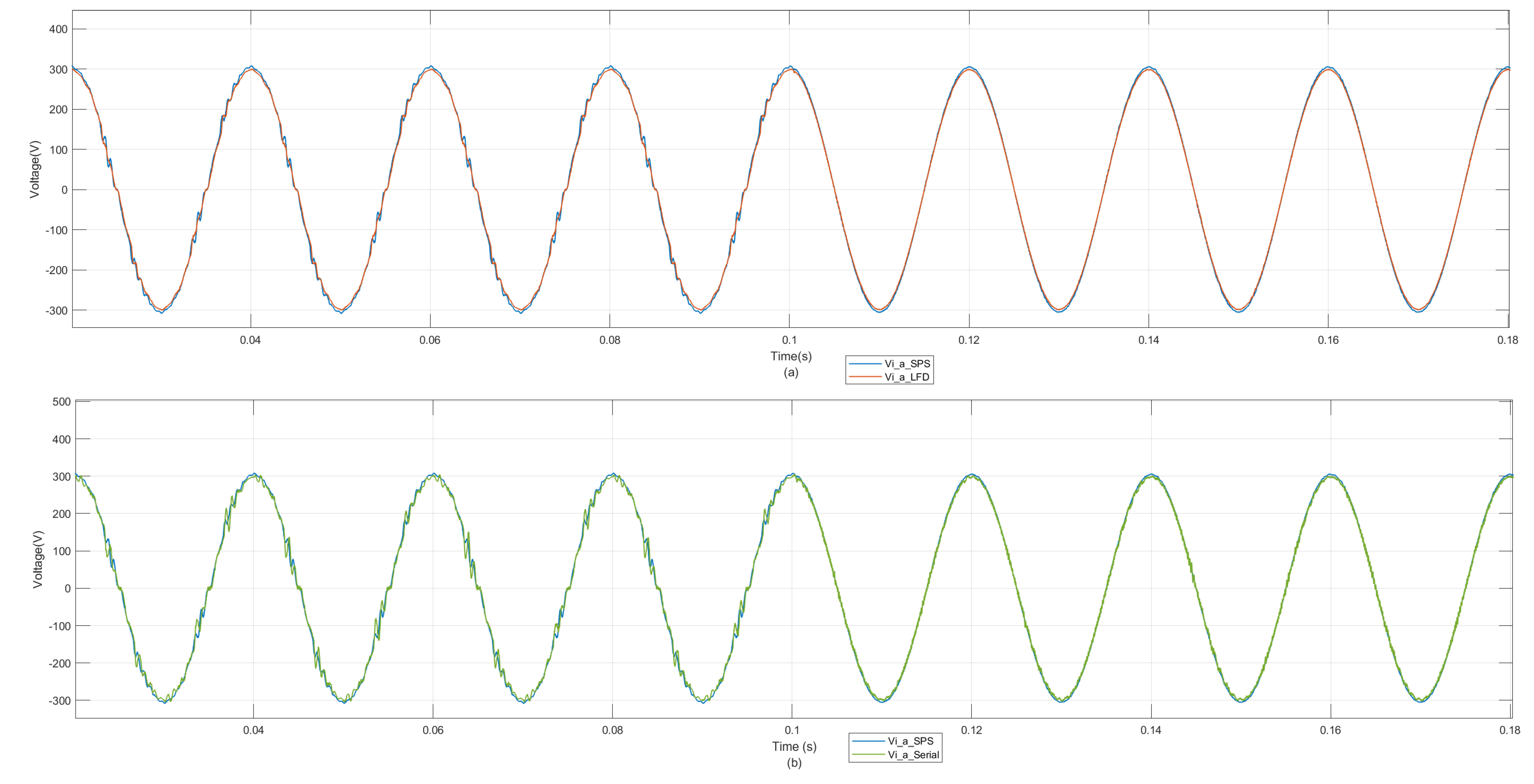
In order to verify the modeling accuracy, we first simulated the model on the FPGA board using the LDF and serial decoupling methods, with both adopting the same simulation parameters as SPS, as shown in Table 1. At the same time, in order to verify the model accuracy, the same control algorithm (FCS-MPC) was adopted, so that the error only resulted from the method proposed in this paper. The LDF model, serial decoupling model and Simulink power system (SPS) model are compared, respectively, and the output current i o , input voltage, V i , and instantaneous reactive power, Q i n , are analyzed. At the same time, in order to verify the effect of instantaneous reactive power tracking of FCS-MPC, the instantaneous reactive power was not tracked before t = 0.1 s (instantaneous reactive power tracking started after t = 0.1 s).
As shown in Figure 12a below, the output current i o of the load-side A-phase output of the SPS model and latency-free decoupling model is shown. The average error of the waveforms of the latency-free decoupling model and the SPS model is 0.01% before 0.1 s, and the average error is 0.03% after 0.1 s. The results of serial simulation with SPS are shown in Figure 12b. The average error is 0.01% before 0.1 s, and the average error is 4.5% after 0.1 s.
The input voltage V i of phase A of the power supply side for the SPS model and the latency-free decoupling model is shown in Figure 13a below. The average error of the waveforms of the latency-free decoupling model and the SPS model is 0.02%. The serial simulation with SPS is shown in Figure 13b. The average error before 0.1 s is 3.4%, and the average error after 0.1 s is 2.7%.
The effects of instantaneous reactive power tracking were also compared, as shown in Figure 14a. It can be seen that the time-free delayed decoupling model can better simulate SPS, after starting tracking after 0.1 s, the value is close to 0, while the serial model produces oscillations near 0. The input and output currents are compared in Figure 14b,c, and it can be seen that delay decoupling does not produce results close to the results of offline simulation SPS, regardless of whether the instantaneous power is tracked or not.

4.3. Resource Consumption and Time Step

The resource consumption is outlined in Table 2, where it can be seen that latency-free decoupling requires more multipliers and registers to realize parallel operation, while serial operation requires more adders and shift-position operators to carry out the computation. In general, the total resource consumption of latency-free decoupling is smaller. In terms of time steps, the minimum delay path determines the minimum number of simulation steps that can be executed by the system. Latency-free decoupling only requires 153.845 ns, representing real-time simulation with a step length of less than 200 ns, while serial decoupling requires 380.254 ns. It is clear that latency-free decoupling can effectively reduce the real-time simulation step length.

5. Conclusions

In this paper, through the method of latency-free decoupling, an overall circuit is divided and decoupled at the capacitor and inductor and parallel computation is adopted in the decoupled circuit. This improves the computation speed, reduces the amount of computation and effectively reduces the resource utilization of the FPGA in real-time simulations. The model was verified in the Speedgoat real-time simulator, and at the same time, to verify the accuracy of the decoupling method, the results of offline simulations and serial real-time simulations were compared. Through the results of this comparison, it can be seen that the speed enhancements brought about by latency-free decoupling are not at the expense of accuracy; on the contrary, compared with serial decoupling, the accuracy is higher and the error rate is lower.

Author Contributions

Conceptualization, Z.S. and S.L.; Methodology, S.L. and Y.H.; Software, X.G.; Validation, X.G. and R.Q.; Investigation, Z.S. and X.G.; Writing—original draft, S.L.; Writing—review & editing, S.L.; Funding acquisition, Y.H. and X.G. All authors have read and agreed to the published version of the manuscript.

Funding

This research was funded by the Nuclear Power Operations Research Institute (NPRI) under the project: Voltage Transformer Online Monitoring and Fault Diagnosis Project Development Technology, Licence No. JYJFY-22006900-000. Furthermore, this research was partially supported by the Xiamen Key Laboratory of Frontier Electric Power Equipment and Intelligent Control.

Data Availability Statement

All data underlying the results are available as part of the article and no additional source data are required.

Conflicts of Interest

The authors declare that there are no conflict of interest.

References

  1. Di, Z.; Xu, D.; Zhang, K. Continuous Control Set Model Predictive Control for an Indirect Matrix Converter. Energies 2021, 14, 4114. [Google Scholar] [CrossRef]
  2. Tawfiq, K.B.; Ibrahim, M.N.; Rezk, H.; El-kholy, E.E.; Sergeant, P. Mathematical Modelling, Analysis and Control of a Three to Five-Phase Matrix Converter for Minimal Switching Losses. Mathematics 2021, 9, 96. [Google Scholar] [CrossRef]
  3. Ramalho, A.W.S.; Vitorino, M.A.; Corrêa, M.B.d.R.; Costa, L.A.L.d.A.C.; Braga-Filho, E.R. New Family of Two-to-Three-Phase AC–AC Indirect Matrix Converters with Open-End Rectifier Stage. IEEE Trans. Ind. Appl. 2022, 58, 517–530. [Google Scholar] [CrossRef]
  4. Garcia, C.F.; Rivera, M.E.; Rodríguez, J.R.; Wheeler, P.W.; Peña, R.S. Predictive Current Control with Instantaneous Reactive Power Minimization for a Four-Leg Indirect Matrix Converter. IEEE Trans. Ind. Electron. 2017, 64, 2. [Google Scholar] [CrossRef]
  5. Varajão, D.; Araújo, R.E. Modulation Methods for Direct and Indirect Matrix Converters: A Review. Electronics 2021, 10, 812. [Google Scholar] [CrossRef]
  6. Gong, Z.; Li, J.; Dai, P.; Su, D.; Wu, X. Design and Evaluation of a Virtual Vector Based Modulated Model Predictive Control for the Indirect Matrix Converters with Improved Performance. IEEE Trans. Ind. Electron. 2022, 69, 12019–12029. [Google Scholar] [CrossRef]
  7. Meddah, K.; Robert, T.; Rutovic, E.; Monthéard, R.; Ould-Bachir, T. Real-Time Simulation of a Neutral Point Clamped Dual Active Bridge Converter. In Proceedings of the 2022 IEEE 1st Industrial Electronics Society Annual On-Line Conference (ONCON), Kharagpur, India, 9–11 December 2022; pp. 1–5. [Google Scholar] [CrossRef]
  8. Matar, M.; Iravani, R. FPGA Implementation of the Power Electronic Converter Model for Real-Time Simulation of Electromagnetic Transients. IEEE Trans. Power Deliv. 2010, 25, 2. [Google Scholar] [CrossRef]
  9. Rødal, G.L.; Peftitsis, D. Real-Time FPGA Simulation of High-Voltage Silicon Carbide MOSFETs. IEEE Trans. Power Electron. 2023, 38, 3213–3234. [Google Scholar] [CrossRef]
  10. Ebrahimi, S.; Amiri, N.; Jatskevich, J. Interfacing of Parametric Average-Value Models of LCR Systems in Fixed-Time-Step Real-Time EMT Simulations. IEEE Trans. Energy Convers. 2020, 35, 1985–1988. [Google Scholar] [CrossRef]
  11. Bieber, L.; Wang, L.; Jatskevich, J.; Li, W. Universal Equivalent Model for Real-Time CPU/FPGA Co-Simulation of Hybrid Cascaded Multilevel Converters. IEEE Access 2023, 11, 4228–4241. [Google Scholar] [CrossRef]
  12. Shin, D.-C.; Lee, D.-M. Development of Real-Time Implementation of a Wind Power Generation System with Modular Multilevel Converters for Hardware in the Loop Simulation Using MATLAB/Simulink. Electronics 2020, 9, 606. [Google Scholar] [CrossRef]
  13. Lee, J.; Kang, D.; Lee, J. A Study on the Improved Capacitor Voltage Balancing Method for Modular Multilevel Converter Based on Hardware-In-the-Loop Simulation. Electronics 2019, 8, 1070. [Google Scholar] [CrossRef]
  14. Kim, M.-n.; Yi, J.-s.; Won, C.-Y.; Lee, J.-H. Methods to Improve Dynamic System Response of Power Compensators Using Supercapacitors in Low-Voltage Ride-Through (LVRT) Conditions. Electronics 2022, 11, 1144. [Google Scholar] [CrossRef]
  15. Milton, M.; Benigni, A. Latency Insertion Method Based Real-Time Simulation of Power Electronic Systems. IEEE Trans. Power Electron. 2018, 33, 7166–7177. [Google Scholar] [CrossRef]
  16. Liu, C.; Ma, R.; Bai, H.; Gechter, F.; Gao, F. A new approach for FPGA-based real-time simulation of power electronic system with no simulation latency in subsystem partitioning. Int. J. Electr. Power Energy Syst. 2018, 99, 650–658. [Google Scholar] [CrossRef]
  17. Xu, J.; Wang, K.; Wu, P.; Li, Z.; Liu, Y.; Li, G.; Zheng, W. FPGA-Based Submicrosecond-Level Real-Time Simulation of Solid-State Transformer with a Switching Frequency of 50 kHz. IEEE J. Emerg. Sel. Top. Power Electron. 2021, 9, 4212–4224. [Google Scholar] [CrossRef]
  18. Grégoire, L.-A.; Blanchette, H.F.; Bélanger, J.; Al-Haddad, K. Real-Time Simulation-Based Multisolver Decoupling Technique for Complex Power-Electronics Circuits. IEEE Trans. Power Deliv. 2016, 31, 2313–2321. [Google Scholar] [CrossRef]
  19. Asai, H.; Tsuboi, N. Multi-Rate Latency Insertion Method with RLCG-MNA Formulation for Fast Transient Simulation of Large-Scale Interconnect and Plane Networks. In Proceedings of the 2007 Proceedings 57th Electronic Components and Technology Conference, Sparks, NV, USA, 29 May–1 June 2007. [Google Scholar] [CrossRef]
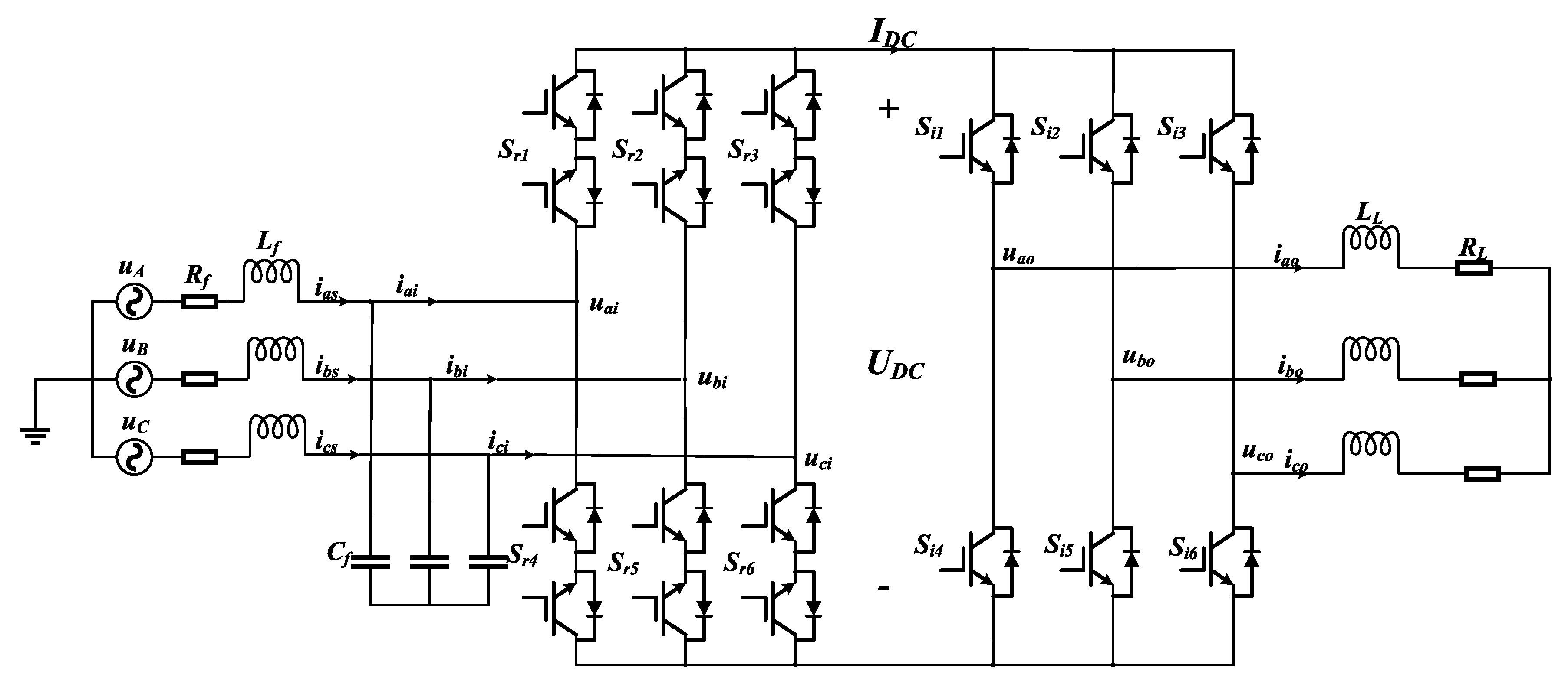
Figure 1. IMC circuit topology.
Electronics 12 04802 g001
Figure 2. FCS−MPC control flow.
Electronics 12 04802 g002
Figure 3. SPS offline simulation: (a) output phase A current, (b) output phase A voltage, (c) input phase A current, (d) input phase A voltage, (e) DC bus voltage.
Electronics 12 04802 g003
Figure 4. System execution: (a) parallel decoupling, (b) serial decoupling.
Electronics 12 04802 g004
Figure 5. Latency−free decoupling method: (a) before decoupling, (b) after decoupling.
Electronics 12 04802 g005
Figure 6. Capacitor−inductor equivalent replacement.
Electronics 12 04802 g006
Figure 7. IGBT switching state judgment.
Electronics 12 04802 g007
Figure 8. Latency-free decoupled modeling process.
Electronics 12 04802 g008
Figure 9. IMC decoupling: (a) power side, (b) rectifier side, (c) inverter side, (d) load side.
Electronics 12 04802 g009
Figure 10. System operation.
Electronics 12 04802 g010
Figure 11. Experimental environment.
Electronics 12 04802 g011
Figure 12. i o current waveform: (a) SPS-LFD comparison (b) SPS-serial comparison.
Electronics 12 04802 g012
Figure 13. V i voltage waveform (a) SPS-LFD comparison (b) SPS-serial comparison.
Electronics 12 04802 g013
Figure 14. Power and output voltage and current waveform. (a) Reactive power waveform, (b) output voltage waveform, (c) input current waveform.
Electronics 12 04802 g014
Table 1. IMC parameters.
VariablesDescriptionValue
u s Supply phase voltage311.1 V
f s Supply frequency50 Hz
L f Input filter inductance400 μ H
C f Input filter capacitance30 μ F
R f Input filter resistance1 Ω
R L Load resistance30 Ω
L L Load inductance10 mH
Table 2. FPGA resource utilization.
Latency-Free DecouplingSerial
Multipliers3424
Adders/Subtractors721921
Registers3831
Total 1-Bit Registers1104592
Multiplexers59717308
I/O Bits954388
Static shift operators0260
Dynamic shift operators9197
Time step (minimum delay path)153.845 ns380.254 ns
Disclaimer/Publisher’s Note: The statements, opinions and data contained in all publications are solely those of the individual author(s) and contributor(s) and not of MDPI and/or the editor(s). MDPI and/or the editor(s) disclaim responsibility for any injury to people or property resulting from any ideas, methods, instructions or products referred to in the content.