Article

Influence of JFET Width on Short-Circuit Robustness of 1200 V SiC Power MOSFETs

1
School of Micro-Nano Electronics, Zhejiang University, Hangzhou 310027, China
2
ZJU-Hangzhou Global Scientific and Technological Innovation Center, Zhejiang University, Hangzhou 311200, China
3
College of Electrical Engineering, Zhejiang University, Hangzhou 310027, China
*
Author to whom correspondence should be addressed.
These authors contributed equally to this work.
Electronics 2023, 12(23), 4849; https://doi.org/10.3390/electronics12234849
Submission received: 8 October 2023 / Revised: 20 November 2023 / Accepted: 28 November 2023 / Published: 30 November 2023

Abstract

:
This paper investigates and compares the static performance and short-circuit (SC) robustness of 1200 V SiC MOSFETs with varying JFET widths (WJFET = 2.0–5.0 μm). Short-circuit measurements as well as electrical-thermal simulations are used to identify thermal distribution and maximum electrical field, providing valuable insights into the design limits. The devices under test (DUTs) with narrow and wide WJFET exhibit different failure mechanisms under SC stress. After the short-circuit failure, interlayer dielectric (ILD) cracks are observed in DUTs with narrow JFET width (WJFET < 3 μm). In contrast, it is discovered that the burn mark is located in the channel region of the device with a wide JFET width. Moreover, the short-circuit withstand time (SCWT) of DUTs with narrow and wide WJFET exhibits varying trends under high temperature conditions (100 °C). These results can help verify the different failure mechanisms and determine an optimal JFET design to improve the trade-off between the static performance and SC ruggedness of the SiC MOSFETs.

1. Introduction

SiC MOSFETs have already emerged as one of the most crucial components in power electronic systems. They can be utilized at frequencies exceeding 100 kHz, which can facilitate a reduction in the volume of passive components and enhance the power density of the system [1]. MOSFETs are gaining increasing popularity in electric vehicles (EVs), hybrid electric vehicles (HEVs), and railways, with a growing interest in their reliability and robustness.
Approximately 38% of inverter failures can be attributed to the failure of power devices induced by short-circuit (SC) stresses [2,3,4]. During the device operation, unexpected circuit faults may occur. For example, in the half-bridge circuit, failures often arise from short circuits in the upper or lower bridge devices, and the device channel may accidentally conduct current when the device withstands the high drain voltage. This high current density flowing through the device can lead to device failure. Numerous investigations have been conducted on the short-circuit characteristics of commercial SiC MOSFETs. The results of the short-circuit test provide valuable information about the SiC MOSFET’s ability to handle short-circuit faults without suffering permanent damage. It helps in determining the device’s short-circuit withstand capability, evaluating the effectiveness of its protection mechanisms, and assessing its thermal management strategies [5]. This knowledge is crucial for designing reliable power electronic systems that utilize SiC MOSFETs and ensuring their safe operation under various fault conditions. The short-circuit performance of SiC MOSFET power modules under various operating conditions has also been studied [6,7]. Compared to Si IGBTs, the short-circuit withstand time (SCWT) of SiC MOSFETs is 80% shorter due to their larger current densities and higher electrical fields [7]. During the short-circuit (SC) process, the heat generated in SiC MOSFETs leads to a rapid increase in the junction temperature, exceeding 1000 °C [8,9]. The rapid increase in junction temperature induces thermal and mechanical stress on the interface between aluminum and the interlayer dielectric. This stress has been observed to cause cracks at the corner of the interlayer dielectric, as reported in references [10,11]. The oxide thickness, Pwell doping and channel length have been extensively studied in SiC MOSFETs [12,13,14]. Channel structure on the short-circuit capability of SiC MOSFETs has been investigated. The impacts of channel design parameters, such as doping profiles and dimensions, are compared, offering guidelines for optimizing the channel structure for enhanced short-circuit performance [15]. The impacts of gate structure on the short-circuit performance of SiC MOSFETs are explored. Different gate designs influence the device’s ability to handle short-circuit events, providing insights into optimizing the gate structure for improved short-circuit withstand time [16]. However, the short-circuit robustness of SiC MOSFET with different JFET widths and the optimal design for JFET width are still under investigation. JFET width is the vital parameter in SiC MOSFET, which not only affects the on-resistance, electrical field at oxide, but also influences the saturate current and short-circuit characteristics. The device researcher always focuses on the optimal parameters in static performance, but the comparison of short-circuit characteristics of switches with different JFET widths needs to be evaluated. Furthermore, devices from various manufacturers have different value (Commercial device of A company has the width of 1.75 μm. Commercial device of B company has the width of 2.8 μm).
In this study, SiC MOSFETs with various structural parameters are fabricated and their impacts on short-circuit capability are investigated. The correlation between short-circuit withstanding time and measurement temperature is studied. Electrical-thermal simulations are used to identify thermal distribution and maximum electrical field, providing valuable insights into the design limits. Additionally, device failure mechanisms are analyzed based on experimental and simulation results for different structure designs. Finally, the optimal structure design of SiC MOSFETs is summarized for improving the trade-off relationship between device conduction performance and short-circuit ruggedness.

2. Materials and Methods

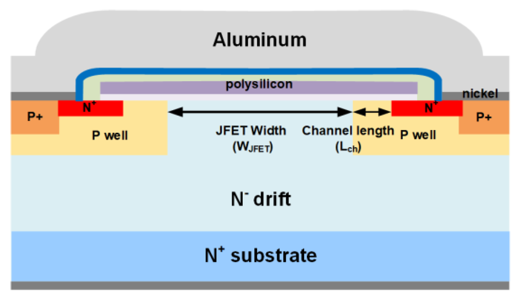
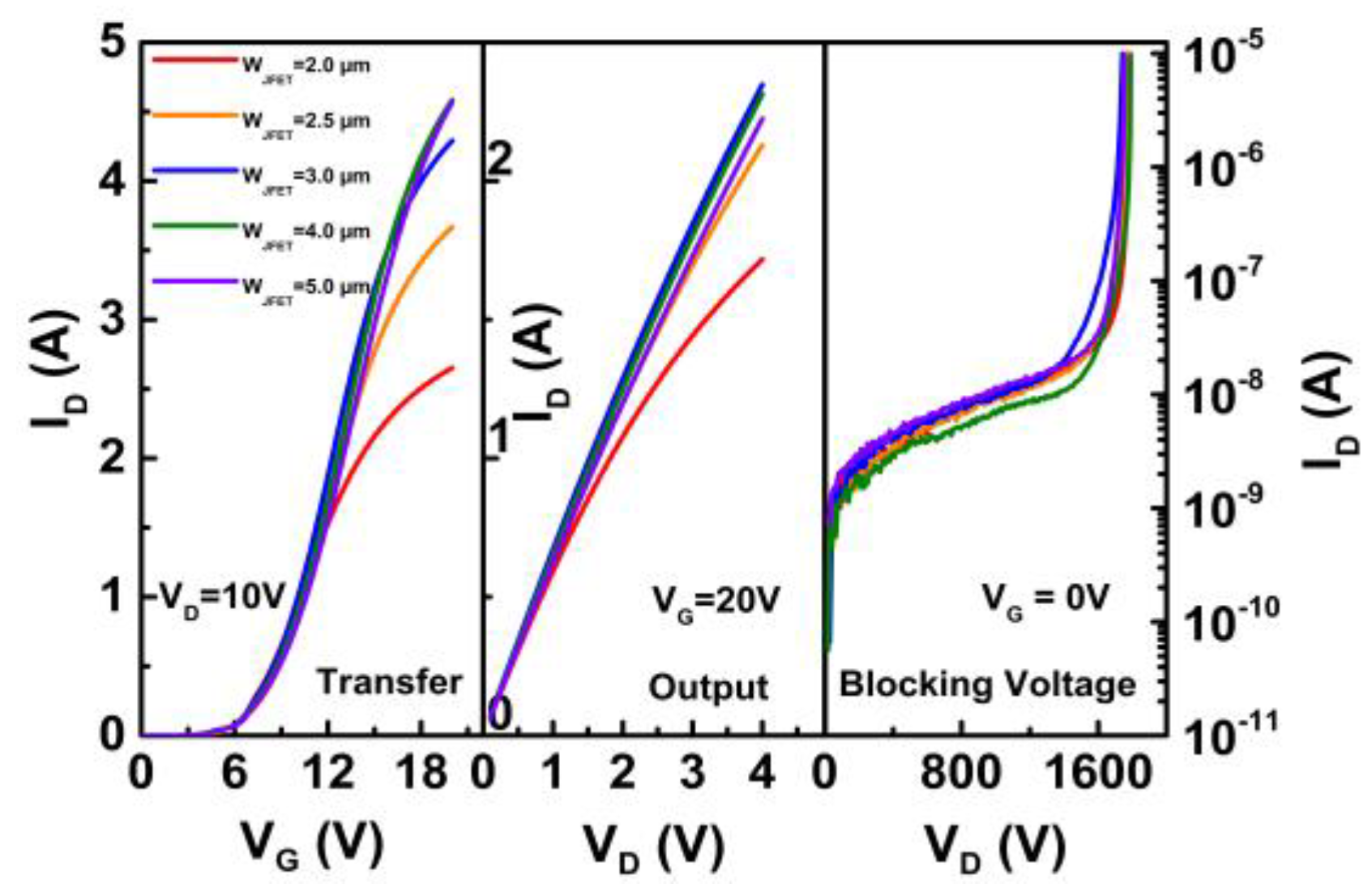
2.1. Static Characteristics of SiC MOSFETs with Different Structural Parameters

As shown in Figure 1, the JFET width (WJFET) is one of the key structural parameters for SiC MOSFETs, which significantly affects both device performance and reliability. To study its impact on short-circuit ruggedness, 1200 V SiC MOSFETs with various WJFET (2.0, 2.5, 3.0, 4.0, and 5.0 μm) are fabricated in this work. In the fabricated SiC MOSFETs, the channel doping is 1 × 1017 cm−3, the drift region doping is 8 × 1015 cm−3 and the drift thickness is 12 μm. The fabrication flow is shown in Figure 2. In SiC MOSFET, the JFET region is located between two adjacent P well regions. And P well—Nepi—P well is like JFET (junction field effect transistor), so this region is named the JFET region. Due to the intrinsic depletion region, the real current path is narrower than the dimension of WJFET. To optimize, the minimal resistance and minimize electrical field are at the center of gate oxide (<3 MV/cm).
The five SiC MOSFET devices in this study are labeled A1–A5. The devices have identical active areas and chip sizes. In this section, the static characteristics of the five MOSFET devices are measured and analyzed.
The transfer, output and blocking I–V (current-voltage) characteristics of the five devices are measured by Keysight B1505A equipment and the results are compared in Figure 3. For the transfer I–V characteristics, the drain-source voltage (VDS) is set to 10 V in the measurement. For the output I–V characteristics, the gate-source voltage (VGS) is set to 20 V. For the blocking I–V characteristics, the VGS is set to 0 V. Device performance indexes, such as threshold voltage, resistance, transconductance and breakdown voltage are extracted and summarized in Table 1.
With increasing WJFET design, the threshold voltage initially decreases from 2.58 to 2.52 V, and then increases to 2.73 V. Correspondingly, the on-resistance decreases from 1.68 to 1.48 Ω, and then increases to 1.6 Ω. The transconductance of the device gradually increases from 0.377 to 0.841 S. Besides, from the blocking characteristics, all five devices can successfully achieve blocking voltages above 1700 V.
The on-resistance of a SiC MOSFET device is composed of channel resistance, JFET region resistance, drift layer resistance and substrate resistance. For 1200 V SiC MOSFETs, JFET region resistance contributes around 30% of the total resistance at room temperature. Increasing the WJFET can help reduce the JFET region resistance. However, it can also result in an increase in the cell pitch and a decrease in channel density, if the source region width remains constant. According to the experimental results, Device A3 with WJFET = 3 μm achieves the lowest resistance of 1.48 Ω among the five designs.
The output characteristics of the five devices are measured at 25 to 175 °C to investigate the conduction performance of SiC MOSFETs at high temperatures. The on-resistances at different temperatures are presented in Figure 4. It can be observed that the on-resistance increases with temperature for all five devices, but the temperature coefficient of resistance varies for different WJFET designs.
The channel resistance of VDMOS is determined by calculating the resistance of lateral long channel MOSFET and converting it based on channel length and width, as seen in Figure 4. The channel resistance accounts for more than 30% of the total resistance. The channel resistance decreases as the temperature increases from room temperature to 175 °C. At higher temperatures, the threshold voltage of the device decreases, resulting in an increased generation of electrons in the channel. Furthermore, higher electron densities in the channel provide a better screening effect, reducing the Coulomb scattering caused by interface traps. These two factors contribute to the overall reduction in channel resistance [12]. Apart from the channel resistance, the bulk resistance exhibits a positive temperature coefficient, which is due to the lower mobility of carries at elevated temperatures caused by acoustic scattering. The opposite temperature behaviors of the channel resistance and bulk resistance components lead to the different trends in total resistance at elevated temperatures for devices with different WJFET. With a narrower JFET width, the JFET resistance becomes a larger proportion of the total resistance. Consequently, the total resistance increases more rapidly at elevated temperatures.
For Device A1, with a narrow WJFET design (2.0 μm), the JFET region resistance contributes significantly to the total on-resistance. It also has a positive temperature coefficient, resulting in the highest slope among the five devices in Figure 3. For Device A5, with a wide WJFET design (5.0 μm), the JFET region resistance contributes only a small portion to the total on-resistance. In contrast, the channel resistance plays a more significant role in determining the overall resistance of Device A5. The negative temperature coefficient of the channel resistance in Device A5 counterbalances the positive temperature coefficient of JFET region resistance, drift layer resistance and substrate resistance. Thus, the slope of the curve for Device A5 in Figure 3 is the lowest among the five devices. For Device A3 to A5, the on-resistances are less sensitive to ambient temperature, which is good for high temperature applications. The slight increase in on-resistance with temperature is beneficial for balancing current in parallel connections.
The devices’resistance types are channel resistance, JFET resistance, drift resistance and substrate resistance, as shown in Figure 4, and the resistance is mainly based. To illustrate the reason for the transconductance and on-resistance exhibiting different trends, the different compositional resistance needs to be separated, as shown in Figure 4b. Transconductance is mainly controlled by channel resistance, as the channel resistance is dependent on the gate voltage. If the channel resistance occupies a larger portion in the on-resistance, the transconductance is higher. In five types of DUTs, the wider WJFET has a larger portion of channel resistance, so the transconductance is higher.
WJFET influence the cell pitch and also have a large impact on JFET resistance. When WJFET decreases, smaller cell pith results in the reduced channel resistance. However, narrower WJFET leads to increased JFET resistance, which is a trade-off in different devices. Among five types of devices, the WJFET = 3 μm is the optimal value.

2.2. Short-Circuit Capability of SiC MOSFETs

A short-circuit (SC) test platform has been established. Figure 5a illustrates the test bench, while Figure 5b presents the schematic diagram of the test board. The device under test (DUT) is connected in series with an IGBT device and a current shunt. A pulsed gate-source voltage is applied to the gate terminal of the DUT, and the duration of the short circuit is controlled by the pulse width. The duration of the short-circuit time gradually increased until the device reaches a failure state. In this section, we compare the short-circuit withstand time (SCWT) of SiC MOSFETs with different WJFET designs. We also analyze the device failure mechanisms, considering various device designs and different bus voltages.

3. Results

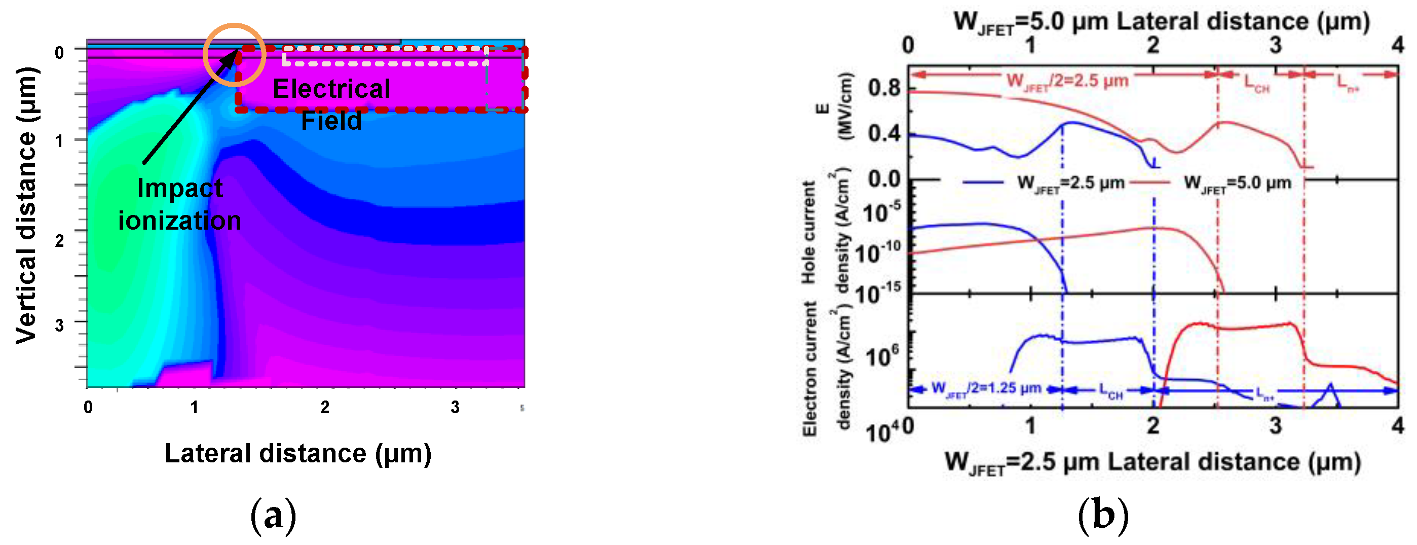
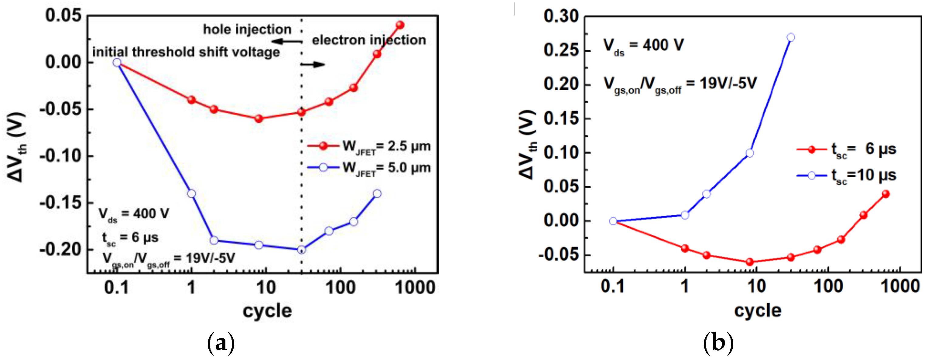
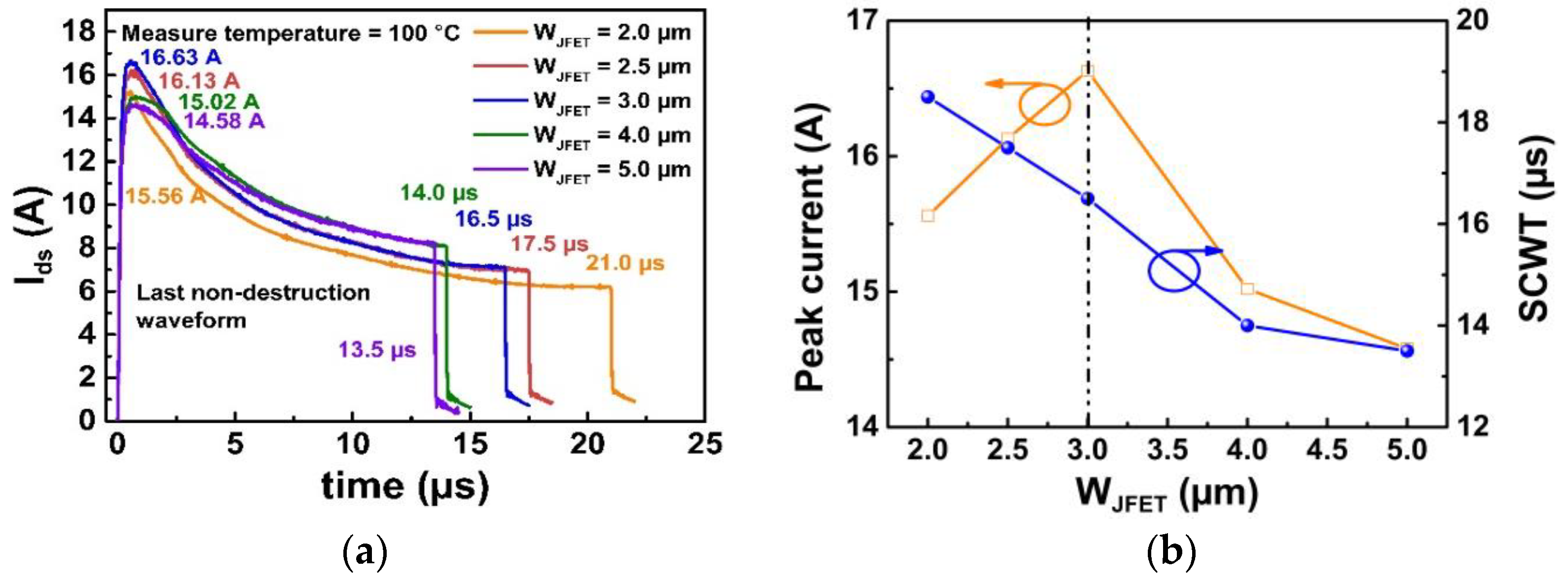
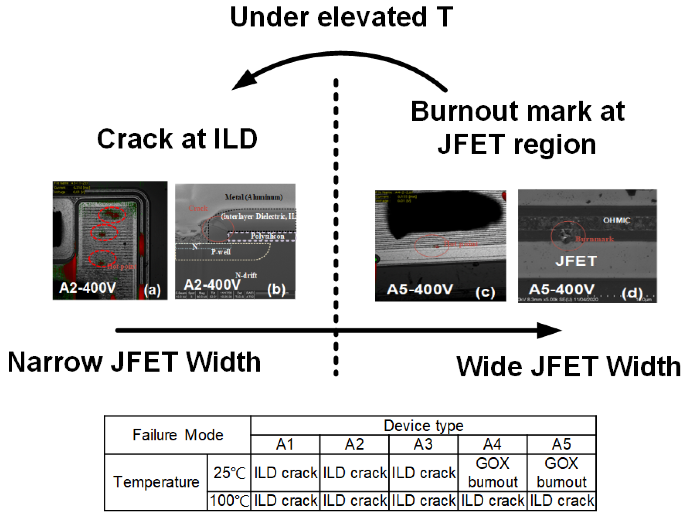
3.1. Short-Circuit Capability of SiC MOSFETs with Different JFET Widths at 400 V

The on and off gate-source voltages (VGS) are 20 and −5 V, respectively. The bus voltage is 400 V, and the short-circuit duration time is increased with a step of 0.5 μs until the device fails. The last non-destruction short-circuit current waveforms for different device designs are illustrated in Figure 6a. According to the figure, the SCWT of Device A1, A2, A3, A4, and A5 are 19.0, 18.5, 17.0, 15.0 and 14.0 μs, respectively. Device A3 with WJFET = 3.0 μm demonstrates the highest peak current due to the lowest on-resistance, as discussed in Section 2. On the other hand, the SCWT gradually decreases with the increase in WJFET. The changes in peak current and SCWT with WJFET are summarized in Figure 6b. The typical waveform of gate voltage and drain current for the destruction test are shown in Figure 6c. After the destruction test, it is observed that the gate is shorted to the source terminal for all five devices. When the WJFET is increased from 2.0 to 3.0 μm, devices with wider WJFET exhibit higher peak currents. The higher peak currents result in increased energy dissipation, which can lead to a rapid rise in junction temperature and a reduction in SCWT. However, when JFET width is further increased from 3.0 to 5.0 μm, both the peak current and SCWT decrease. It is evident that wide WJFET design devices are likely to experience different failure mechanisms compared to devices with narrower WJFET designs.
The failure mode is checked with blocking characteristic measurements after device failure, which are shown in Figure 7. After device failure, Device A2 with WJFET = 2.5 μm remains almost the same blocking voltage (Figure 7a) as a fresh device, while Device A5 with WJFET = 5.0 μm shows degraded blocking capability (Figure 7b). OBIRCH (Optical Beam Induced Resistance Change) is utilized to find out the failure spot. The failure spot in Device A2 is located in the active region, as shown in Figure 8a. FIB (Focus Ion Beam) analysis is employed to observe the cross-section at the failure spot. Figure 8b displays the obtained cross-sectional result of Device A2. Cracks are observed in the ILD (interlayer dielectric) between gate polysilicon and source metal in Device A2. However, for Device A5, different observations are shown. The failure spot is also observed in the active region, as shown in Figure 8c. When the device is stripped in solvents to expose the SiC layer’s surface, a burn mark is found between the JFET region and the channel region. The top view of the device is illustrated in Figure 8d.
To explain the failure mechanism, the TCAD is used to simulate the short-circuit procedure in SiC MOSFETs. The SiC/SiO2 interface mobility model is established, taking into account the presence of interface traps. The integration of the interface trap is coulomb charge named Nc. Varying the interface trap density at the SiC/SiO2 interface leads to differences in the short-circuit current waveform, as demonstrated in Figure 9a. With the lower interface trap density, the peak current is higher, and more heat is generated in the SiC MOSFET. The interface trap distribution is determined by extracting the interface trap from the MOS capacitance. Figure 9b shows the comparison between the simulation results (using Dit = 3 × 1011 cm−2eV−1) and the corresponding measurement results. The simulation model is established and the temperature can be extracted through the simulation.
For Device A2, the cracks found at ILD are due to the unmatched coefficient of thermal expansion (CTE) between different materials [17]. With higher temperatures, the CTE becomes larger [18,19]. The temperature distribution during the SC procedure at the ILD corner is calculated using a simulation tool, and the result is shown in Figure 10. Consequently, the dominant failure mechanism is the junction temperature rise caused by the energy dissipation within the device during the short-circuit pulse.
For Device A5, the failure mode could be different. To investigate the failure mode, the short-circuit transient process is simulated using TCAD. Due to the wide WJFET design, the electrical field at SiC surface (upper in JFET region) is higher than that in Device A2, resulting in a higher impact ionization. The impact ionization within Device A5 is shown in Figure 11a. Higher impact ionization leads to an increase in hole and electron current densities. A comparison of the hole and electron current densities can be seen in Figure 11b. As the electric field direction points from SiC to the gate in the JFET region, the holes would inject into the gate oxide due to the combined effect of electric field and high kinetic energy resulting from the elevated temperature. Additionally, in the channel region, the channel electron density in Device A5 is also higher than that in Device A2. Both the holes in the JFET region and electrons in the channel region have the potential to degrade the gate oxide and lead to device failure. To identify the main reason, a repetitive short-circuit test is conducted. The voltage shift direction indicates whether there is hole injection (negative shift) or electron injection (negative shift). Device A2 and Device A5 are measured during a repetitive short-circuit test with Vds = 400 V, a pulse width of 6µs and Vgs,on/Vgs,off = 19 V/−5 V. When the cycle time is low, the device with a wider JFET width is influenced more by hole injection than electron injection, as observed in the comparison of the two devices in Figure 12a. However, Device A2 is primarily affected by electron injection. With repetitive cycle increasing, the electron injection becomes dominant due to the hot electron effect, as shown in Figure 12b.

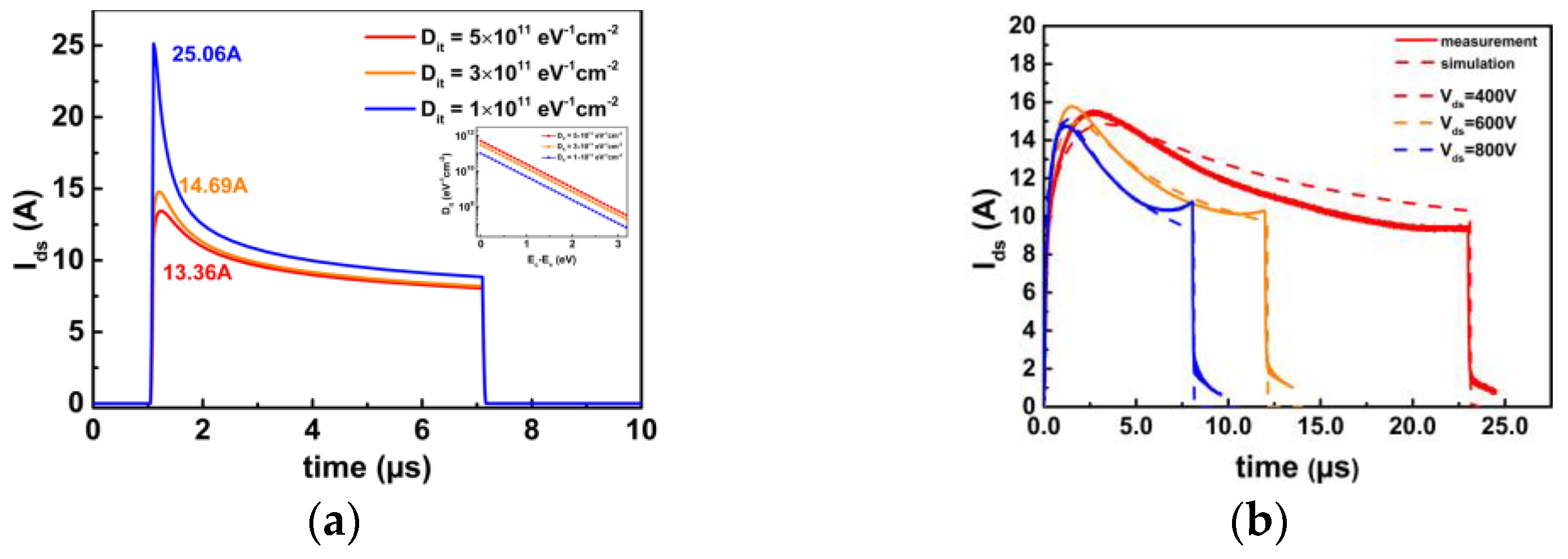
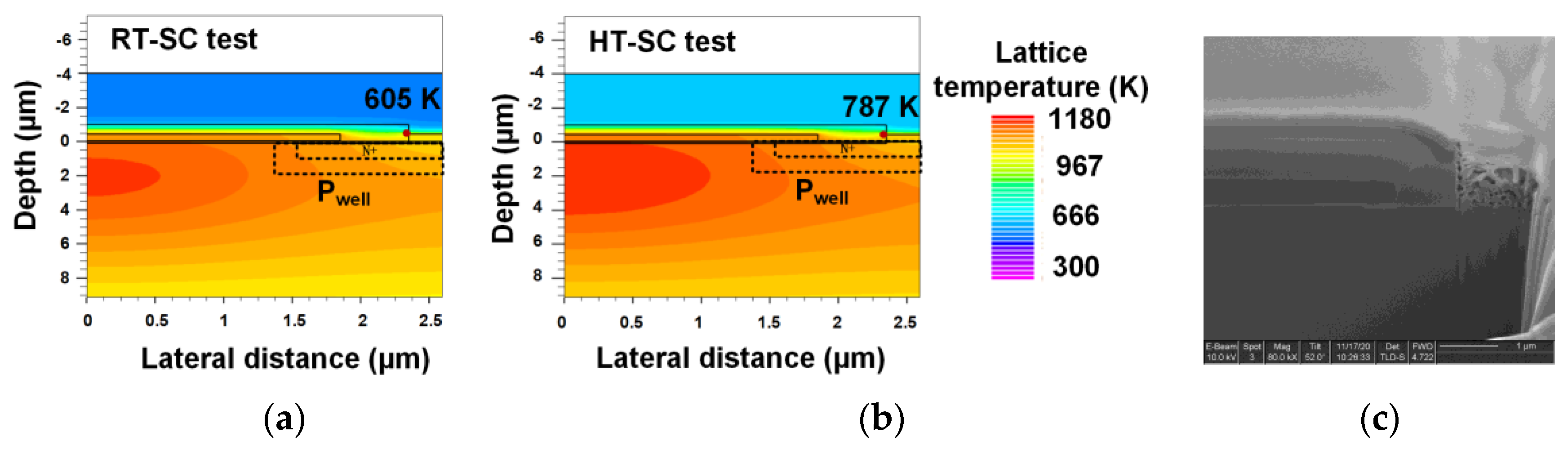
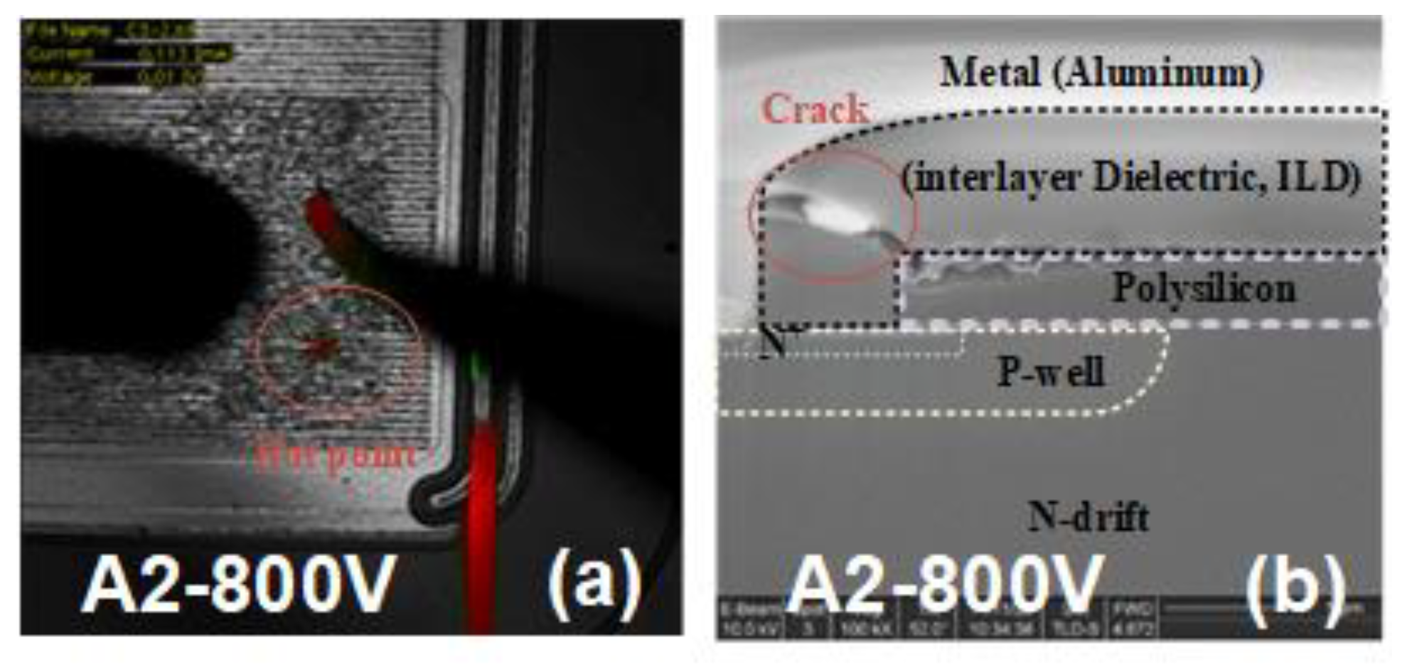
3.2. Short-Circuit Capability of SiC MOSFETs Measured at Elevated Temperature

Short-circuit tests are carried out at an ambient temperature of 100 °C to verify the failure mechanisms for Device A2 and Device A5. The SC current waveforms are shown in Figure 13a. The peak current and SCWT for the five WJFET designs are extracted from the figure and summarized in Figure 13b. The correlations between SC peak current (SCWT) and WJFET observed at 100 °C are similar to the results obtained at 25 °C (refer to Figure 6b).
To study the impacts of ambient temperature on SCWT test results for different WJFET designs, the results obtained at 25 °C and 100 °C test conditions are compared in Figure 14a. The results indicate that wide WJFET designs (WJFET ≥ 3 μm) exhibit an increase in SCWT at elevated temperatures—namely, SCWT demonstrates a positive temperature coefficient for wide WJFET designs. The increase in SCWT can be attributed to reduced electron injection into the gate oxide at elevated temperatures. Figure 14b compares the short-circuit current waveforms for the 25 and 100 °C test conditions, with tsc = 3 μs used as an example. The peak current at 100 °C is lower than that of 25 °C due to the limitations of acoustic scattering at elevated temperatures, resulting in reduced election injection for the 100 °C test condition.
On the other hand, for narrow WJFET designs (WJFET < 3.25 μm), SCWT decreases at elevated temperatures. The junction temperature is calculated using simulation software. Figure 15 shows the temperature distribution within the device during the short-circuit transient at both 25 °C (Figure 15a) and 100 °C (Figure 15b). Elevated ambient temperatures result in higher junction temperatures. The thermal and mechanical stress can cause cracks in ILD layers, and higher temperatures result in a larger coefficient of thermal expansion mismatch [11]. Thus, the SCWT is decreased at elevated temperatures. In order to figure out whether failure mechanism is changed in the device with wider WJFET, failure spot of Device A4 after SC test under 100 °C is detected shown in Figure 15c. Compared with the results shown in Figure 8b, the ILD crack becomes the main failure reason for the device with wide WJFET.

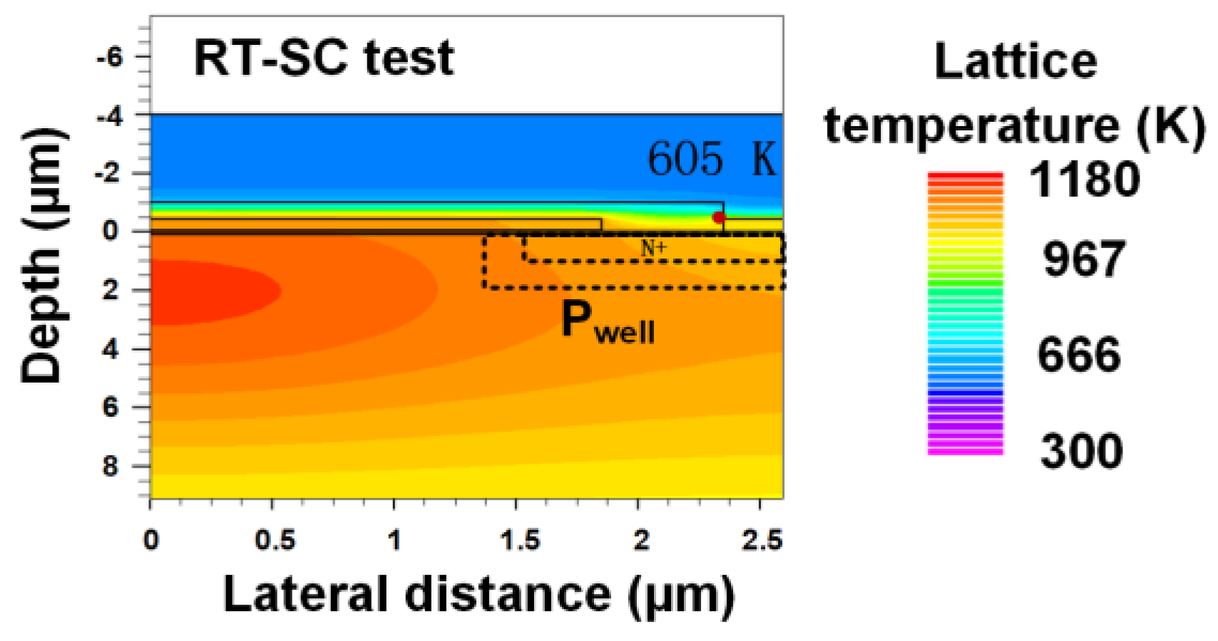
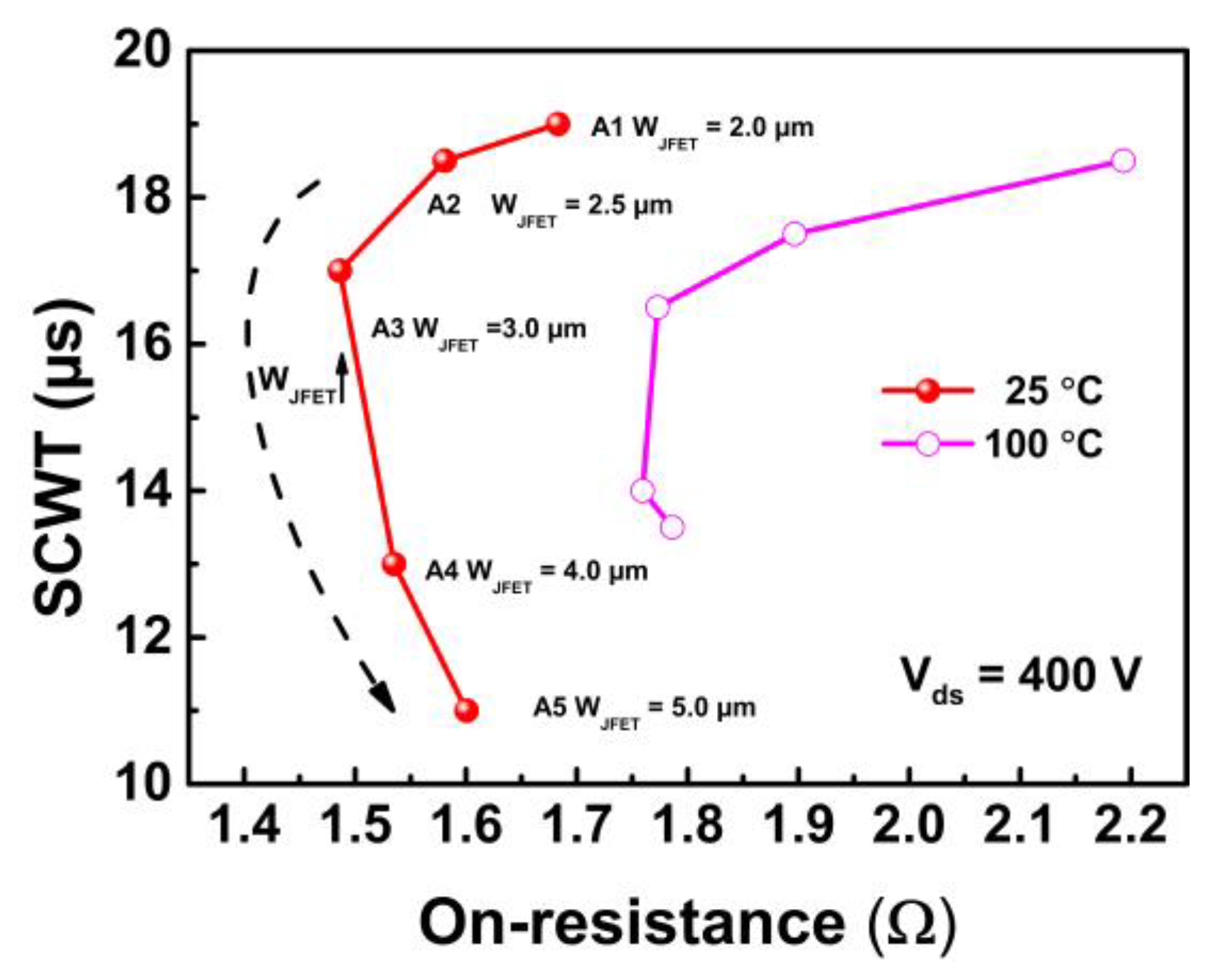
3.3. Short-Circuit Capability of SiC MOSFETs with Different JFET Widths at Varied Vds Measured at Room Temperature

The SC capability of SiC MOSFETs is measured under different bus voltages (400, 600 and 800 V). The short-circuit pulse width (tSC) is gradually increased from 3 μs in steps until DUT fails. The increment step is set to 0.5 μs for 400 V, 0.3 μs for 600 V and 0.1 μs for 800 V, respectively. The short-circuit current waveforms for the five devices tested under a high bus voltage of 800 V are illustrated in Figure 16. The peak current varies among different WJFET designs. For Device A1–A3 with narrow WJFET designs, the peak current is higher than the other two designs, resulting in a shorter SCWT. Additionally, in Device A2, an interlayer crack is observed after the SC test under 800 V in Figure 17a,b.
The SCWT tested under different bus voltages is summarized in Figure 18a. The energy can be calculated using short-circuit current waveforms and device voltage waveforms. The calculated results are plotted in Figure 18b. Devices with different JFET widths have almost the same SCWT under drain voltages of 600 and 800 V. The WJFET has a significant effect on the SCWT when the drain voltage is 400 V. For higher bus voltage conditions, the difference in SCWT among the five designs is significantly reduced. In addition, at higher bus voltages, the maximum short-circuit energy that device can safely dissipate is reduced to 33%, as shown in Figure 18b. This is because the short-circuit current multiplied by a high bus voltage generates a significant amount of heat on a very short time scale (<1 μs), causing the device junction temperature to rise rapidly. Thus, the SCWT and total energy are decreased.

4. Discussion

The on-resistance and short-circuit withstanding time are crucial parameters for SiC MOSFETs, representing their conduction performance and reliability, respectively. It has been reported that the structure designs (JFET region width in this work) can influence both the on-resistance and short-circuit withstanding time. Furthermore, there exists a trade-off relationship between the on-resistance and SCWT, which will be discussed in this section. Figure 19 summarizes the on-resistance and SCWT parameters for each device (Device A1–A5 with different WJFET designs). The SCWT test results for the three bus voltage conditions (400, 600 and 800 V) are also illustrated in the figure. For each bus voltage, increasing the WJFET from 2 to 3 μm results in a decrease in device on-resistance from 1.68 to a minimum of 1.48 Ω (a reduction of 11.9%). However, a further increase in WJFET will raise the on-resistance, which is unacceptable. On the other hand, observing the SCWT parameters for the 400 V bus voltage condition (red lines in Figure 19), we can observe a slight drop from Device A1 to A3 (11.7%), followed by a significant drop from A3 to A5 (35.2%). The impact of WJFET designs on SCWT is negligible for higher bus voltages. The bus voltage is usually determined by the power electronic system and circuit designs in practical applications. The saturation current primarily indicates the short-circuit current. The short-circuit current and saturation current are positively correlated. In SiC MOSFETs, the saturation current is influenced by two factors: the JFET region’s pinch-off voltage and the MOSFET channel’s saturation voltage. Short-circuit simulations are used to evaluate the potential under the gate oxide. With a wider JFET width, the potential at the JFET side increases, leading to an increase in channel saturation current due to the Drain-Induced Barrier Lowering effect. Additionally, a lower pinch-off voltage results in a smaller saturation current in the JFET region. When the JFET region becomes sufficiently narrow, the saturation current of the JFET region becomes the primary factor. For 1200 V–rated SiC MOSFETs, the bus voltage can be selected between 400~800 V or even out of this range. In conclusion, the optimal design of WJFET is 3 μm for the 1200 V SiC MOSFETs studied in this work, without considering an enhanced doping concentration for the JFET region.
Under high bus voltage conditions, devices with various JFET widths exhibit similar short-circuit behavior. As the JFET region becomes depleted during the short-circuit test, the resistances in the JFET region become relatively small compared to the channel resistance. Therefore, the JFET width has less impact on the result. Furthermore, it can be concluded that the variation in JFET width is not highly sensitive to the short-circuit withstand capability under high bus voltage, but it exhibits a greater impact under low bus voltage conditions. Moreover, Device A3 demonstrates the best performance within the voltage range of 400 to 800 V.
The relationship between the short-circuit test results at temperatures of 25 and 100 °C and the on-resistance under a 400 V bus voltage is shown in Figure 20 and will be discussed in the following paragraphs. In Section 3.2, the failure reason for DUTs under a high-temperature SC test is clarified. Failure mode is summarized in Figure 21. The failure of a wide WJFET device is due to gate oxide burnout tested in SC under room temperature. As the temperature increases, the failure mode changes to the ILD crack. When the temperature is above 100 °C, the device failure mode becomes the same. When evaluating the performance of devices operated at high temperatures, the static resistance gradually increases with temperature, while the short-circuit duration time at high temperatures varies. The devices with wider WJFET inhibit the injection of hot electrons at an elevated temperature, thereby reducing the formation of defects caused by hot carriers. Therefore, there is an improvement in SCWT. When the width of the JFET is less than 3.0 μm (A3), due to the increase in the junction temperature in the high-temperature test, the temperature in the interlayer dielectric reaches the critical value faster, resulting in a reduction in the short-circuit withstand time. If the temperature rises to 150 °C, the SCWT for WJFET devices may all decrease due to the failure mode being changed to the ILD crack mode.
Judging from the trade-off relationship between the on-resistance and short-circuit current at room temperature and high temperature, devices with WJFET larger than 3.0 μm are more suitable for operating at high temperatures. These devices exhibit a gradual increase in resistance at high temperatures, resulting in an improved short-circuit performance to a certain extent.

5. Conclusions

In this paper, 1200 V SiC MOSFETs with various WJFET are fabricated, followed by a comprehensive comparison and study of the short-circuit robustness of these devices. Devices with narrow and wide WJFET exhibit distinct failure mechanisms. The ILD crack is observed in the device with narrow WJFET, while the breakdown of gate oxide is found in the device with wider WJFET after device failure. The relationship between on-resistance and SCWT of devices A1–A5 with different JFET widths is summarized. Device A3 demonstrates the best performance in terms of SCWT and on-resistance characteristics, making it an improved design. Furthermore, devices with narrowed JFET widths have limitations in improving SCWT (<20 μs) under a bus voltage of 400 V. The relationship between the short-circuit test results at temperatures of 25 and 100 °C and on-resistance under a bus voltage of 400 V is also investigated. Devices with WJFET larger than 3.0 μm exhibit improved SCWT under high temperatures and are better suited for high temperature operation. As the temperature rises, their resistance shows a slow increment, contributing to an enhanced short-circuit performance to a certain degree.

Author Contributions

Conceptualization, N.R. and K.S.; data curation, H.X.; formal analysis, H.X. and B.W.; funding acquisition, K.S.; investigation, H.X.; methodology, B.W. and H.X.; project administration, N.R. and K.S; resources, N.R., K.H. and K.S.; software, H.X. and B.W.; supervision, N.R.; validation, B.W. and H.L.; visualization, H.X.; writing—original draft, H.X.; writing—review and editing, H.X. and B.W. All authors have read and agreed to the published version of the manuscript.

Funding

This research was funded by grants from the Department of Science and Technology of Zhejiang Province: 2022C01235.

Institutional Review Board Statement

Not applicable.

Informed Consent Statement

Not applicable.

Data Availability Statement

Data are contained within the article.

Acknowledgments

The authors (H.X., N.R., J.W., Z.Z., Q.G. and K.S.) thank the Technology Innovation and Training Center, Polytechnic Institute, Zhejiang University, Hangzhou, Zhejiang Province, China, for providing the Keysight B1505A power devices analyzer equipment.

Conflicts of Interest

The authors declare no conflict of interest.

References

  1. Chen, Z.; Huang, A.Q. High Performance SiC Power Module Based on Repackaging of Discrete SiC Devices. IEEE Trans. Power Electron. 2023, 38, 9306–9310. [Google Scholar] [CrossRef]
  2. Fuchs, F. Some diagnosis methods for voltage source inverters in variable speed drives with induction machines a survey. In Proceedings of the IECON’03. 29th Annual Conference of the IEEE Industrial Electronics Society (IEEE Cat. No. 03CH37468), Roanoke, VA, USA, 2–6 November 2003. [Google Scholar] [CrossRef]
  3. Jiang, X.; Wang, J.; Lu, J.; Chen, J.; Yang, X.; Li, Z.; Tu, C.; Shen, Z.J. Failure modes and mechanism analysis of SiC MOSFET under short-circuit conditions. Microelectron. Reliab. 2018, 88–90, 593–597. [Google Scholar] [CrossRef]
  4. Wang, J.; Jiang, X.; Li, Z.; Shen, Z.J. Short-Circuit Ruggedness and Failure Mechanisms of Si/SiC Hybrid Switch. IEEE Trans. Power Electron. 2018, 34, 2771–2780. [Google Scholar] [CrossRef]
  5. Ahmed, M.T. Performance and Reliability Evaluation of SiC Power MOSFETs for Electric Vehicle Applications. IEEE Trans. Transp. Electrif. 2020, 6, 96–106. [Google Scholar]
  6. Kumar, A.; Losito, M.; Moradpour, M.; Gatto, G. Evaluation of Short-Circuit Capability of SiC MOSFET Power Modules. In Proceedings of the 2022 International Symposium on Power Electronics, Electrical Drives, Automation and Motion (SPEEDAM), Sorrento, Italy, 22–24 June 2022; pp. 523–527. [Google Scholar] [CrossRef]
  7. Moradpour, M.; Pirino, P.; Losito, M.; Franke, W.-T.; Kumar, A.; Gatto, G. Multi-Objective Optimization of the Gate Driver Parameters in a SiC-Based DC-DC Converter for Electric Vehicles. Energies 2020, 13, 3720. [Google Scholar] [CrossRef]
  8. Zhang, S. Short-Circuit Failure Mechanism and Reliability Analysis of SiC MOSFETs. IEEE Trans. Device Mater. Reliab. 2022, 23, 581–589. [Google Scholar]
  9. Sun, J.; Yang, S.; Xu, H.; Zhang, L.; Wu, X.; Sheng, K.; Chen, K.J. High-Temperature Characterization of a 1.2-kV SiC MOSFET Using Dynamic Short-Circuit Measurement Technique. IEEE J. Emerg. Sel. Top. Power Electron. 2020, 8, 215–222. [Google Scholar] [CrossRef]
  10. Sun, J.; Wei, J.; Zheng, Z.; Wang, Y.; Chen, K.J. Short Circuit Capability and Short Circuit Induced VTH Instability of a 1.2-kV SiC Power MOSFET. IEEE J. Emerg. Sel. Top. Power Electron. 2019, 7, 1539–1546. [Google Scholar] [CrossRef]
  11. Liu, J.; Zhang, G.; Wang, B.; Li, W.; Wang, J. Gate Failure Physics of SiC MOSFETs Under Short-Circuit Stress. IEEE Electron Device Lett. 2020, 41, 103–106. [Google Scholar] [CrossRef]
  12. Yao, K.; Yano, H.; Tadano, H.; Iwamuro, N. Investigations of SiC MOSFET Short-Circuit Failure Mechanisms Using Electrical, Thermal, and Mechanical Stress Analyses. IEEE Trans. Electron Devices 2020, 67, 4328–4334. [Google Scholar] [CrossRef]
  13. Agarwal, A.; Kanale, A.; Han, K.; Baliga, B.J.; Bhattacharya, S. Impact of Gate Oxide Thickness on Switching and Short Circuit Performance of 1200 V 4H-SiC Inversion-channel MOSFETs. In Proceedings of the 2019 IEEE 7th Workshop on Wide Bandgap Power De-vices and Applications (WiPDA), Raleigh, NC, USA, 29–31 October 2019; pp. 59–62. [Google Scholar] [CrossRef]
  14. Bencherif, H.; Dehimi, L.; Pezzimenti, F.; Yousfi, A.; De Martino, G.; Della Corte, F.G. Impact of a non-uniform p-base doping concentration on the electrical characteristics of a low power MOSFET in 4H-SiC. In Proceedings of the 2019 International Conference on Advanced Electrical Engineering (ICAEE), Algiers, Algeria, 19–21 November 2019; pp. 1–4. [Google Scholar] [CrossRef]
  15. Chen, Y. Effect of Channel Structure on Short-Circuit Capability of SiC MOSFETs. IEEE Electron Device Lett. 2023, 44, 1166–1169. [Google Scholar]
  16. Zhang, M. Impact of Gate Structure on the Short-Circuit Performance of SiC MOSFETs. IEEE Trans. Electron Devices 2023, 70, 1380–1386. [Google Scholar]
  17. Romano, G.; Riccio, M.; Maresca, L.; Breglio, G.; Irace, A.; Fayyaz, A.; Castellazzi, A. Influence of design parameters on the short-circuit ruggedness of SiC power MOSFETs. In Proceedings of the 2016 28th International Symposium on Power Semiconductor Devices and ICs (ISPSD), Prague, Czech Republic, 2–16 June 2016; pp. 47–50. [Google Scholar] [CrossRef]
  18. Tachiki, K.; Ono, T.; Kobayashi, T.; Tanaka, H.; Kimoto, T. Estimation of Threshold Voltage in SiC Short-Channel MOSFETs. IEEE Trans. Electron Devices 2018, 65, 3077–3080. [Google Scholar] [CrossRef]
  19. Baliga, B.J. Material properties and transport physics. In Fundamentals of Power Semiconductor Devices; Springer: Raleigh, NC, USA, 2008; pp. 23–28. [Google Scholar]
Figure 1. The schematic diagram of the 1200 V SiC MOSFET.
Electronics 12 04849 g001
Figure 2. Manufacture flow of the 1200 V SiC MOSFET.
Electronics 12 04849 g002
Figure 3. Static characteristics of SiC MOSFETs with different JFET widths.
Electronics 12 04849 g003
Figure 4. (a) Compositional channel resistance and total resistance at elevated temperature. (b) Compositional resistance in Device A1.
Electronics 12 04849 g004
Figure 5. (a) Short-circuit test bench. (b) Schematic diagram of the SC test board.
Electronics 12 04849 g005
Figure 6. (a) The SC current waveforms of five types of devices with different JFET widths at Vds = 400 V. (b) Extracted SC peak current and SCWT in devices with varied JFET widths. (c) Failure waveform including gate and drain waveforms.
Electronics 12 04849 g006
Figure 7. Blocking characteristic after short-circuit failure. (a) Device A2 with WJFET = 2.5 μm. (b) Device A5 with WJFET = 5.0 μm.
Electronics 12 04849 g007
Figure 8. (a) The hot spot is observed under OBIRCH (Optical Beam Induced Resistance Change) of Device A2 at drain voltage of 400 V. (b) The cross-section at hot spot is prepared by FIB (Focus Ion Beam) of Device A2 at drain voltage of 400 V. (c) The hot spot is observed on Device A5 at drain voltage of 400 V. (d) Top view of the failure spot of Device A5 at drain voltage of 400 V after the ILD and top metal is dissolved.
Electronics 12 04849 g008
Figure 9. (a) Different interface trap density is established by applying coulomb scattering considering interface trap model. (b) Comparison between measurement and simulation result by using proper model.
Electronics 12 04849 g009
Figure 10. Simulated ILD and source metal temperature during the SC procedure.
Electronics 12 04849 g010
Figure 11. (a) Impact ionization in Device A5 WJFET = 5.0 μm. (b) Comparison of electrical field and hole current density at surface between Device A2 (WJFET = 2.5 μm) and Device A5 (WJFET = 5.0 μm).
Electronics 12 04849 g011
Figure 12. (a) Threshold voltage shift of device with different WJFET after repetitive short-circuit test. (b) Threshold voltage shift for different short-circuit pulse widths (6 and 10 μs).
Electronics 12 04849 g012
Figure 13. (a) The SC current waveforms of five types of devices with different JFET widths at Vds = 400 V at elevated temperature (100 °C). (b) Extracted SC peak current and SCWT in devices with varied JFET widths at elevated temperature (100 °C).
Electronics 12 04849 g013
Figure 14. (a) Relationship between SCWT and JFET width under 25 and 100 °C. (b) Comparison of SC current at 25 and 100 °C under the SC duration time of 3 µs.
Electronics 12 04849 g014
Figure 15. Simulated ILD and source metal temperature during the SC procedure under (a) room temperature and (b) the elevated temperature. (c) The cross-section at hot spot is prepared by FIB (Focus Ion Beam) of Device A5 at drain voltage of 400 V after SC test under 100 °C.
Electronics 12 04849 g015
Figure 16. The SC current waveforms of five types of devices with different JFET widths at Vds = 800 V.
Electronics 12 04849 g016
Figure 17. (a) The hot spot is observed under OBIRCH (Optical Beam Induced Resistance Change) of Device A2 at drain voltage of 800 V. (b) The cross-section at hot spot is prepared by FIB (Focus Ion Beam) of Device A2 at drain voltage of 800 V.
Electronics 12 04849 g017
Figure 18. (a) The SCWT of five types of devices with different JFET widths. (b) The SC energy of five types of devices with different JFET widths.
Electronics 12 04849 g018
Figure 19. The relationship between on-resistance and SC withstanding time (SCWT) of different devices with varied JFET width.
Electronics 12 04849 g019
Figure 20. The relationship between on-resistance and SC withstanding time (SCWT) of devices with varied JFET width at 25 and 100 °C.
Electronics 12 04849 g020
Figure 21. Summary of the failure mode of devices with different WJFET.
Electronics 12 04849 g021
Table 1. Static characteristics of SiC MOSFETs with different JFET widths.
DeviceA1A2A3A4A5
WJFET (μm)2.02.53.04.05.0
Threshold Voltage (V)
(Vd = 10 V, Vth @ Ids = 1 × 10⁻³ A)
2.582.562.522.692.73
On-resistance (Ω)1.681.581.481.531.60
Transconductance (S)0.3770.6020.7480.8370.841
Breakdown voltage (V)
(Vds @ Ids = 1 × 10⁻⁶ A)
17741725174217061777
Disclaimer/Publisher’s Note: The statements, opinions and data contained in all publications are solely those of the individual author(s) and contributor(s) and not of MDPI and/or the editor(s). MDPI and/or the editor(s) disclaim responsibility for any injury to people or property resulting from any ideas, methods, instructions or products referred to in the content.

