Article

Design and Analysis of a Multi−Carrier Orthogonal Double Bit Rate Differential Chaotic Shift Keying Communication System

1
College of Automation and Electrical, Shenyang Ligong University, Shenyang 110159, China
2
College of Information Science & Engineering, Shenyang Ligong University, Shenyang 110159, China
*
Author to whom correspondence should be addressed.
Electronics 2023, 12(8), 1785; https://doi.org/10.3390/electronics12081785
Submission received: 2 March 2023 / Revised: 3 April 2023 / Accepted: 7 April 2023 / Published: 10 April 2023
(This article belongs to the Section Microwave and Wireless Communications)

Abstract

:
A new multi−carrier orthogonal double bit rate differential chaotic shift keying (MC−ODBR−DCSK) communication system is presented in this paper. With two composite signals generated by an orthogonal chaotic signal generator as reference signals, 2M bits of information data are transmitted on M−channel subcarriers, improving transmission speed and energy efficiency. In addition, the receiver does not require a radio frequency (RF) delay circuit to demodulate the received data, which makes the system easier to implement. This paper analyzes Data−energy−to−Bit−energy Ratio (DBR) of the system. The bit error rate performance of the system is simulated to verify the impact of parameters such as chaotic maps, semi-spread spectrum factor, and sub-carrier number. At the same time, the bit error rate performance of the MC−ODBR−DCSK system is compared with traditional DCSK systems in Rician fading and additive Gaussian white noise (AWGN) channels.

1. Introduction

Chaotic signals are random-like, non-periodic, and spread spectrum signals, which make them a good carrier of communication information [1,2,3]. Chaotic digital modulation techniques have simple circuits, which are not easily intercepted and are resistant to the adverse effects of the channel, so it has potential applications in secure communications [4,5].
Differential chaotic shift keying systems have become a hot research topic due to the use of non-coherent modulation techniques [6]. However, in a DCSK system, the bandwidth efficiency, energy efficiency, and data rate are inadequate because the reference signal is transmitted by fifty percent of the bit duration [7]. An efficient differential chaotic shift keying (HE−DCSK) scheme is proposed, which can carry 2 bits of data in a data modulated sample sequence, improving double efficiency [8]. With a time reversal operation generating a reference signal orthogonal to the data carrier signal, an improved DCSK (I−DCSK) system demonstrates [9]; the two sequences of data and reference are combined into a single time slot, which doubles the data rate and improves spectral efficiency. To improve the bit error rate performance of the OFDM−DCSK system, ref. [10] presents a long short-term memory based OFDM−DCSK (LSTM−OFDM−DCSK) system.
In order to combat the eavesdropping or malicious attacks due to the broadcast characteristics of wireless communication system, a MIMO communication system assisted by FH−OFDM−DCSK is designed [11] to advance the security of the MIMO communication system. A multi-user OFDM-DCSK system reduces the integration complexity of the system and improves the spectral efficiency [12]. To enhance data rate and energy efficiency of the DCSK system, a series of improved schemes are implemented [13,14,15].
Several systems improve the security of DCSK systems [16,17]. Multi−carrier Differential Chaos Shift Keying (MC−DCSK) is proposed in [18], which can be considered as a parallel extension of the DCSK system. To improve the bit rate of the MC−DCSK system, a series of optimization schemes are proposed in [19]. In [20], the peak-to-average power ratio (PAPR) of this system is reduced. In [21], an analog network coding multi-user MC−DCSK (ANC−MU−MC−DCSK) system is demonstrated. Compared to the traditional DCSK system, the MC−DCSK system achieves better spectral efficiency and more effective energy consumption while reducing inter-signal interference. In [22], a MC−DCSK system with sparse code spreading (SCS−MC−DCSK) is proposed to improve the efficiency and reliability of multi-user transmission. In [23], a multi-carrier chaotic modulation scheme is proposed, which has good robustness in time-varying underwater acoustic (UWA) channels.
The main contributions of this paper are as follows:
Firstly, we propose a new multi-carrier orthogonal double-speed differential chaotic shift keying (MC−ODBR−DCSK) communication system. In the system, the transmission information is divided into two parts: A and B. Each part corresponds to L group of information, and each group of information corresponds to M subcarriers. The symbol A of one carrier is compounded with the chaotic reference signal, and the symbol B and the chaotic signal through the orthogonal chaotic signal generator (OCG) are compounded and then superimposed with the symbol A to form a carrier, carrying the symbol A and symbol B information, respectively. To realize the information transmission of the two symbols, each subcarrier transmits 1 bit more information than the MC-DCSK communication system.
Secondly, DBR of the MC−ODBR−DCSK system is derived, and energy efficiency of system are analyzed. Compared with DCSK and MC−DCSK system, MC−ODBR−DCSK saves transmitted bit energy and increases data rate.
Thirdly, through simulation analysis, we find that the MC−ODBR−DCSK system improves the transmission data rate and has a better bit error rate than SR-ODBR-DCSK, ODBR−DCSK and DCSK systems under specific signal-to-noise ratio.

2. System Model of MC−ODBR−DCSK

The primary disadvantage of DCSK systems is that they allocate half of the bit duration to transmit non-information-bearing reference samples, which results in a lower data rate and reduced energy efficiency. Higher data rates and energy efficiency are the core goals when designing new chaos-based communication systems. To improve energy efficiency and transmission rates, an improved MC−ODBR−DCSK system is proposed in this paper. This section introduces several key components of the system, including the chaotic signal generator, quadrature device, signal structure, and the transceiver of the MC−ODBR−DCSK system.

2.1. Chaotic Signal Generator

Due to its noise-like characteristics, chaotic signals have good confidentiality as carrier signals, and have become a research hotspot in the field of communication. The chaotic signal generation model for chaotic digital modulation systems is generated by chaotic system mapping. The following will focus on several commonly used chaotic maps.

2.1.1. Sine Map

All trigonometric functions have complex nonlinear dynamics; a Sine Map is evolved from the ordinary sinusoidal trigonometric functions. The specific mathematical expression formula is:
x i + 1 = a 4 sin ( π x i ) ( a ( 0 ,   4 ] )
A Sine Map multiplies the variable x i by π to change the value range of the variable from [0, π] to [0, 1] for easy processing. The parameter a 4 is used as the only parameter and ranges from a 4 ∈ [0, 1].

2.1.2. Improved Logistic Map

Based on the study of the basic composition of a Logistic map, scholars put forward a new Logistic map sequence, that is, an improved Logistic map. The specific mathematical expression formula is:
x i + 1 = 1 μ x i 2                     ( 1 < x i < 1 ,   0 < μ 2 )
The improved Logistic map is similar to the Logistic map in that different systems of parameters are in different states. However, when the value range of μ in the improved Logistic map is μ [ 1.4 ,   2 ] , the system will have chaotic behavior, which is different from the value range of the chaotic state parameters in the Logistic map. When the initial value of iteration is x 0 = 0.40 and the parameter is μ = 2 , the time domain diagram of the map is shown in Figure 1a.

2.1.3. Circle Map

A Circle map is also called a circumference map. The specific mathematical expression formula of a Circle map is:
x i + 1 = x i + a mod ( b 2 π sin ( 2 π x i ) , 1 ) a = 0.5 ; b = 2.2

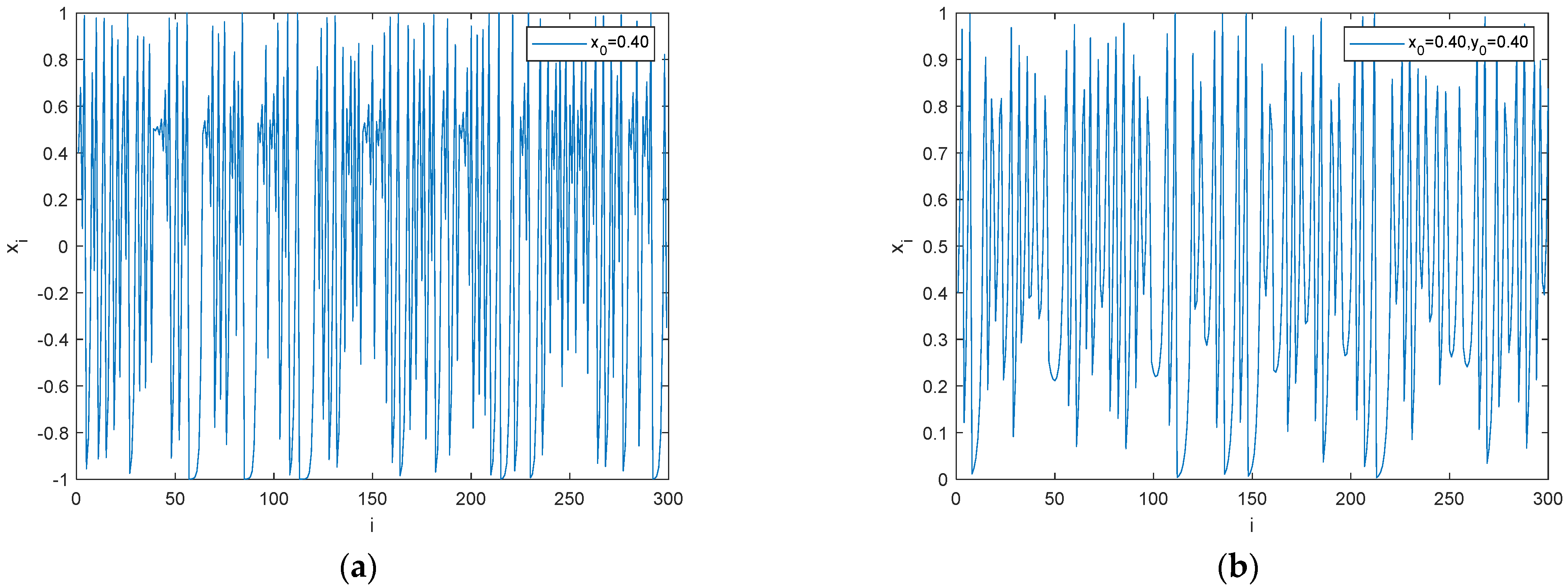
2.1.4. Two-Dimensional Logistic (2D-Logistic) Map

The 2D-Logistic chaotic map is obtained by increasing the dimension of the Logistic map, which is defined as:
{ x i + 1 = r ( 3 y i + 1 ) x i ( 1 x i ) y i + 1 = r ( 3 x i + 1 ) y i ( 1 y i )
where, the control parameter r satisfies r ∈ [0, 2]. When the initial value of iteration is ( x 0 , y 0 ) = ( 0.40 ,   0.40 ) and the parameter r = 1.19 , the time domain diagram of the map is shown in Figure 1b.
As can be seen from Figure 1, the time-domain waveform of a chaotic signal exhibits noise-like characteristics, and as a carrier signal, it has good confidentiality.

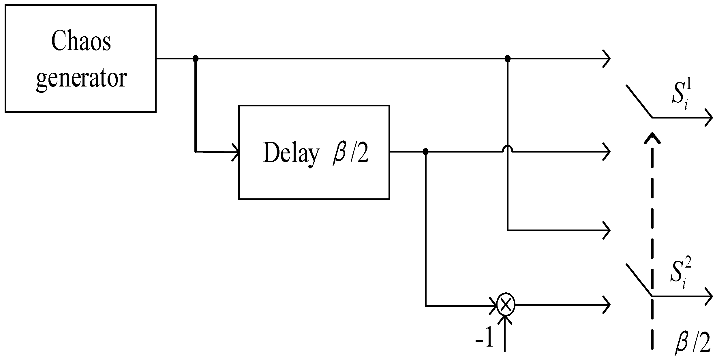
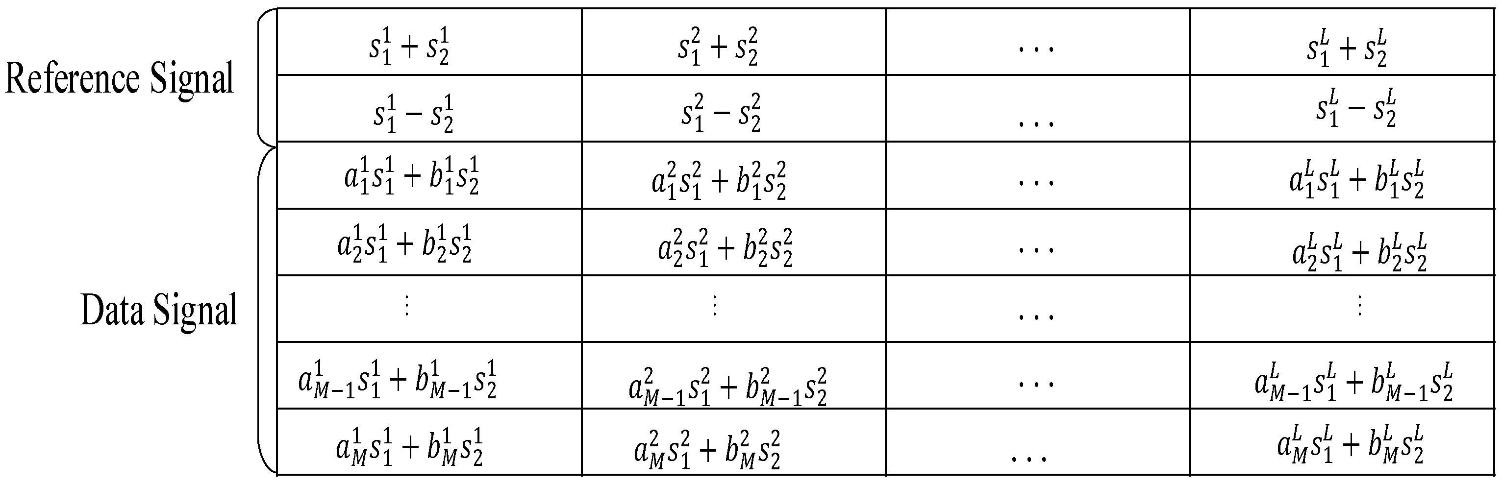
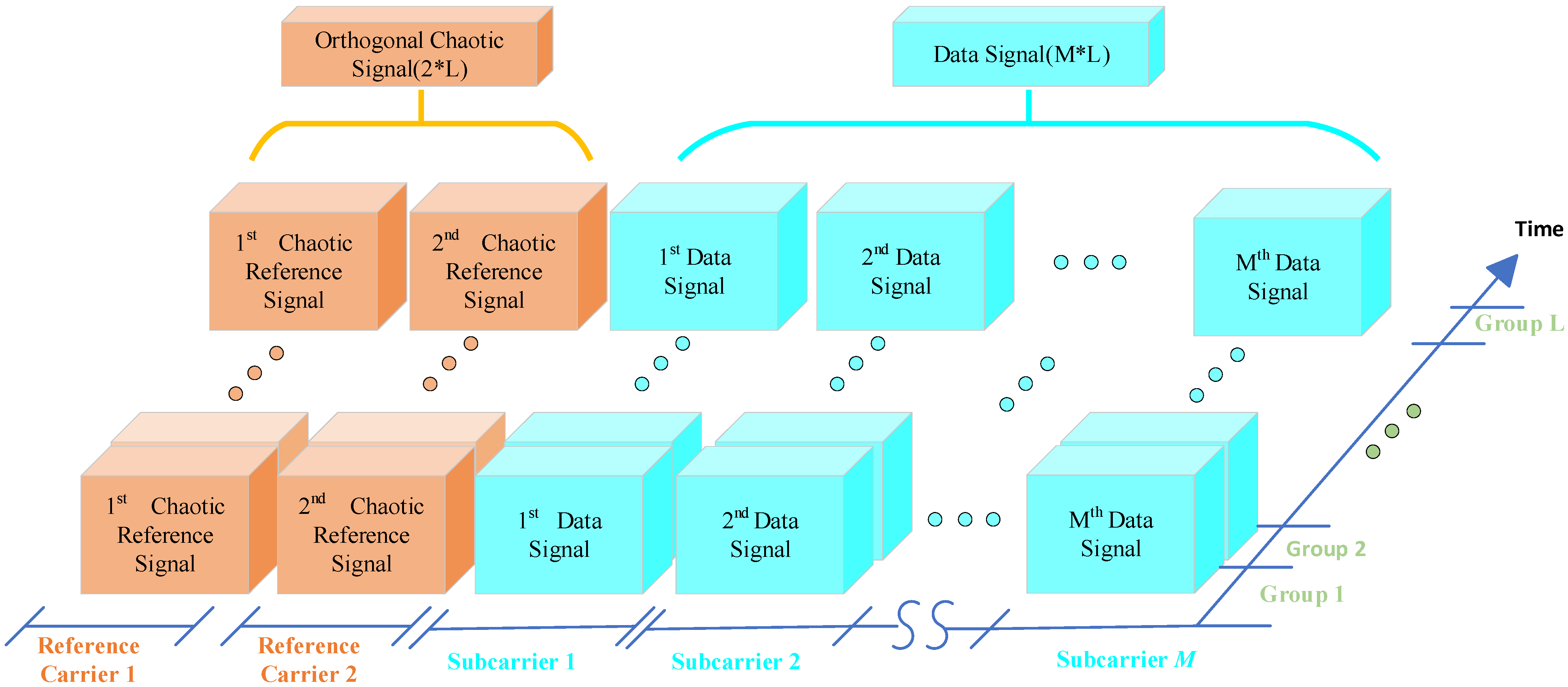
2.2. Transmitter Structure of MC−ODBR−DCSK

To avoid intra-signal interference in the proposed system, we utilize an orthogonal chaotic signal generator (OCG) to produce two distinct chaotic signals. Figure 2 provides a visual representation of the OCG’s block diagram. The OCG generates a pair of orthogonal chaotic carriers that correspond to the two bits of information transmitted in the same information slot. This is achieved through the formulation of specific parameters, as depicted in Figure 2 [24].
s i 1 = s i β / 2 1   , m β < i m β + β / 2
s i 2 = s i β / 2 2   , m β < i m β + β / 2
where s i 1 and s i 2 are the output of the OCG, β is the spreading factor. Furthermore, the relationship between s i 1 and s i 2  i is given as follows:
i = m β + 1 ( m + 1 ) β s i 1 s i 1 = 0 , m , n = 0 , 1 , 2 ,
The experimental parameters are set based on the 3GPP LTE technical report. The transmission bandwidth is assumed to be a fixed value of B, the MC-ODBR-DCSK system divides the bandwidth B into N s u b subcarriers and the number of subcarriers is less than that of Fourier transform points when OFDM modulation is performed. The N s u b subcarriers are divided into L groups, and each group has M + 2 subcarriers. The two subcarriers located in the middle are used to transmit the reference signal, and the rest of the subcarriers in the group are used to transmit data information. The number of subcarriers N s u b , the number of groups L, and the number of subcarriers M + 2 in each group satisfy the relation N s u b  = L × (M + 2). The modulator structure of the MC−ODBR−DCSK system is shown in Figure 3.
The transmitter generates the data to be sent: A and B. The binary message code elements to be sent are   A = [ a 1 , a 2 , , a M × L ] and   B = [ b 1 , b 2 , , b M × L ] . Through serial parallel conversion, it can be converted to A M × L , B M × L :
A M × L = [ a 1 1 a 1 L a M 1 a M L ]             B M × L = [ b 1 1 b 1 L b M 1 b M L ]
In the process of L-group data transmission, the signal structure of the information transmitted in each group is the same, and in order to clearly and intuitively understand the signal transmission process, take one of the groups as an example: l (l = 1, 2, …, L) group. a k l (k = 1, 2, …, M) denotes the kth data bit in the lth group, and a k l is modulated by the chaotic reference signal s 1 l . This process can be understood as a spreading process. The binary data bits b k l (k = 1, 2, …, M) are modulated with the chaotic signal s 2 l formed by the reference signal passing through the OCG. The two sets of modulated data information are summed up correspondingly, and M data information and two reference information form the transmitted signal of the lth set. The ith spreading sample point of the kth information in the lth group can be represented as a k l s 1 i l + b k l s 2 i l . a k l s 1 i l + b k l s 2 i l (i = 1, 2, …, β) can be used as the information format of the Mth subcarriers carrying data in the lth group. The signal format of the reference subcarrier formation l group is added to the data subcarrier, which is converted by IFFT, transmitted, and then sent to the wireless communication channel by parallel-serial conversion. By analyzing and combining the modulation block diagram, it can be found that the MC−ODBR−DCSK system can transmit 2M bits of information in one symbol cycle. In order to show the signal forms in group lth more visually, a diagram of the MC−ODBR−DCSK signal structure is shown in Figure 4.
The signal structure includes a reference signal and an information time signal. The reference signal is composed of two subcarriers generated by the chaotic generator s 1 l and the orthogonal generator s 2 l for addition and subtraction operations. Each group of information signals is divided into M subcarriers. Each subcarrier is composed of data a k l multiplied by the signal s 1 l generated by the chaotic generator, and data b k l multiplied by the orthogonal generator s 2 l and superimposed.
In the MC−ODBR−DCSK system, M subcarriers are employed to transmit multiple data symbols in a parallel way so that a higher data rate could be achieved. As a T−R based system, MC−ODBR−DCSK transmits 2 chaotic signals as the reference signals in one group. Meanwhile, 2M different data signals are transmitted over by M subcarriers. As a result, chaos synchronization circuit is not needed by this receiver since the reference signals. The chaotic signals, are available. In addition, wideband delay line is not needed either, since the reference and data-bearing signals are separated over orthogonal channels. For visualization, Figure 5 shows the format of the transmitted signal of the MC−ODBR−DCSK.
According to the signal structure shown in Figure 4 and Figure 5, MC−ODBR−DCSK system transmits 2 times more bits than MC−DCSK system.

2.3. Receiver Structure of MC−ODBR−DCSK

The transmitter block diagram and signal structure of the transmitter are described in the previous section, and this subsection describes the structure of the receiver of the MC−ODBR−DCSK system. Because of the combination of OFDM key technology, the system does not need a delay circuit, channel estimation, and equalizer when setting up the receiver, and the structure has changed compared to the traditional DCSK technology. The structure of the receiver is the opposite process of the transmitter, and similar to the transmitter. The demodulation process is the same for all groups of signals at the receiver. Again, the analysis of the received signal of group l is used as an example to be able to make the process clearly understood. The block diagram of the receiving end of the MC−ODBR−DCSK system is shown in Figure 6.
The received signal is converted by series-parallel and FFT transform, and the matrix is obtained by FFT transform. The two subcarriers located in the middle of each group are summed and normalized to obtain the reference signal r r e f 1 l of one of the branches, which is deposited into the reference matrix   R 1 l . The reference signal sequence r r e f 1 l is stored in matrix R 2 l through r r e f 2 l generated by the orthogonalizer, and other M information r k l   ( k = 1 , 2 , , M ) in each group is stored in matrix W l . According to the above analysis, the expressions of reference matrix R 1 l , R 2 l and information matrix W l are:
R 1 l = s 1 l + n 1 l
R 2 l = s 2 l + n 2 l
W l = [ a 1 l s 1 l + b 1 l s 2 l + n 1 , 1 l a 2 l s 1 l + b 2 l s 2 l + n 2 , 1 l a M l s 1 l + b M l s 2 l + n M , 1 l ]
n i   represents the noise impact received during transmission. The received data information and reference information are calculated by the matrix product   d ^ 1 , l = sign ( R 1 l × W l ) , d ^ 2 , l = sign ( R 2 l × W l ) (“×” denotes the multiplication operation of two matrices and “′” denotes the transpose operation of the matrix). The original binary information is recovered through the positive and negative results. The demodulation process is as follows:
z k l | a k l = i = 0 β 1 ( a k l s 1 , i l + b k l s 2 , i l + n k , i l ) × ( s 1 , i l + n i l )
z k l | b k l = i = 0 β 1 ( a k l s 1 , i l + b k l s 2 , i l + n k , i l ) × ( s 2 , i l + n i l )
n k , i l   and n i l are two independent Gaussian noise sequences from information slots and reference slots, respectively. The structures of the above two equations are similar, so one group is selected for analysis. By deformation of Equation (12), we can get:
z k l | a k l = i = 0 β 1 [ a k l ( s 1 , i l ) 2 ] + i = 0 β 1 b k l s 1 , i l s 2 , i l + i = 0 β 1 ( s 1 , i l n k , i l + a k l s 1 , i l n i l + b k l s 2 , i l n i l + n i l n k , i l )
where:
z 1 = i = 0 β 1 [ a k l ( s 1 , i l ) 2 ]
z 2 = i = 0 β 1 b k l s 1 , i l s 2 , i l
z 3 = i = 0 β 1 ( s 1 , i l n k , i l + a k l s 1 , i l n i l + b k l s 2 , i l n i l + n i l n k , i l )
The Equation (14) can be divided into three parts, which can solve the useful part z 1 of the original signal. The chaotic signals generate the correlation part z 2 , which generates the internal interference between signals. The third part z 3 is the correlation between the chaotic signal and noise, as well as between the two independent noise. According to the characteristics of mutually independent noise and chaotic signals, the values of z 2 and z 3 can be calculated, because the value of the cross-correlation characteristic is 0. The actual structure of demodulation will be determined by Part z 1 . The positive and negative of a k affect the positive and negative of z 1 , and z 1 ultimately affects the positive and negative of the overall formula. If the transmitted information bit is “+1”, item 1 is a positive value; if the transmitted information bit is “−1”, item 1 is a negative value. Therefore, the decision threshold is set to 0, and the transmitted information will be determined according to the positive and negative of the related reception.
a ^ k l = s i g n [ z k l | a k l ]
b ^ k l = s i g n [ z k l | b k l ]
Information bits can be recovered according to decision rules
a ^ k l = { + 1         [ z k l | a k l ] > 0   1     [ z k l | a k l ] 0  
b ^ k l = { + 1         [ z k l | b k l ] > 0   1     [ z k l | b k l ] 0  

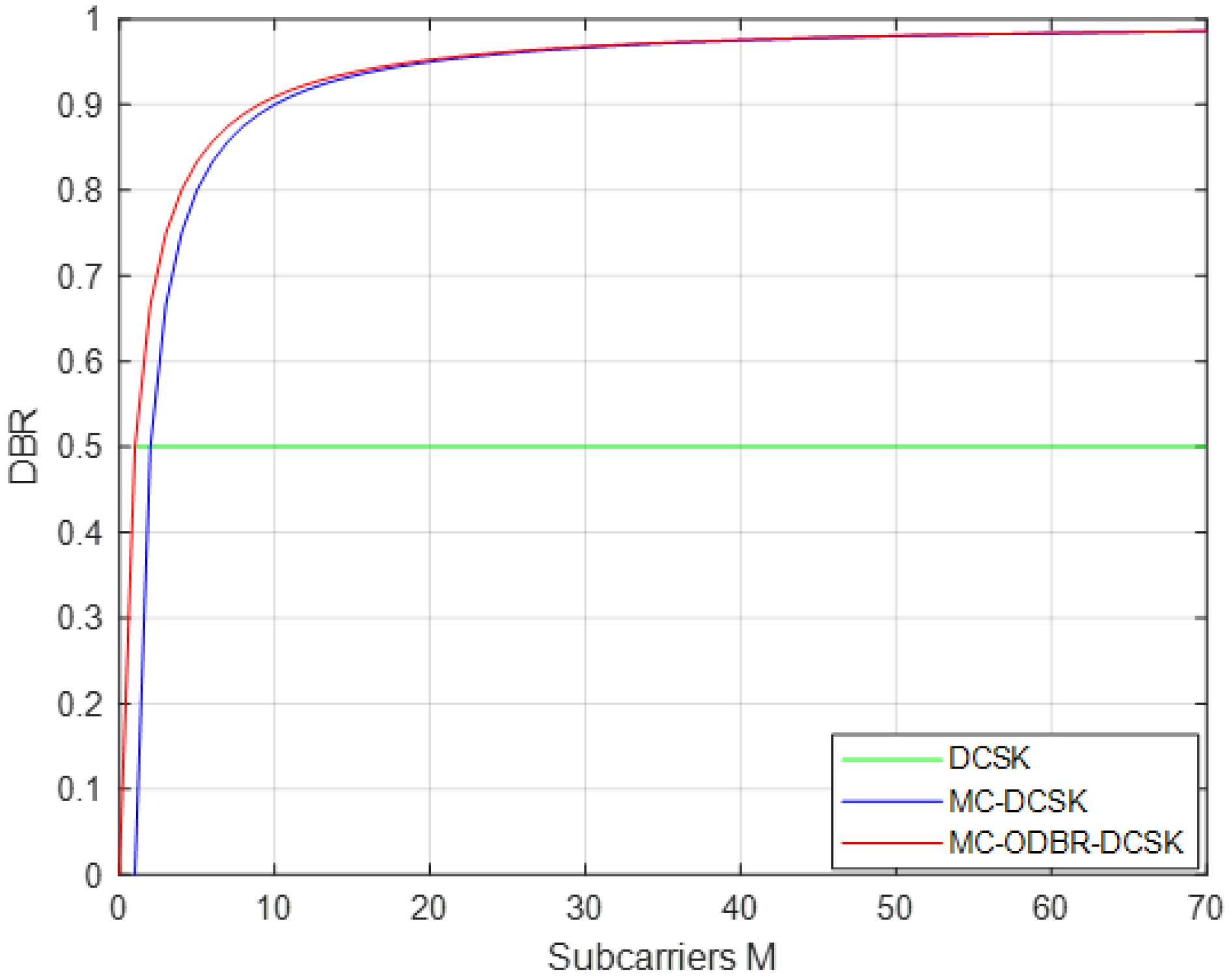
3. Energy Efficiency of the MC−ODBR−DCSK System

In this section, the energy efficiency of the MC−ODBR−DCSK system in a Gaussian channel is analyzed.
The proposed system boasts improved energy efficiency when compared to the DCSK system. In the DCSK system, a new chaotic reference is generated for every transmitted bit, whereas in our case, one reference is shared with M modulated bits. As a result, the transmitted bit energy E b 1 for a conventional DCSK system is:
E b 1 = E r e f + E d a t a
We discuss the energies required to transmit data and reference signals, denoted as E d a t a and E r e f , respectively. Without a loss of generality, the data and the reference energies are equal:
E r e f = E d a t a = j = 0 β 1 x j 2
In the DCSK system, the transmitted energy E b 1 for a specific bit i can be expressed as:
E b 1 = 2 E d a t a = 2 j = 0 β 1 x j 2
The MC−ODBR−DCSK system utilizes two reference energies, which are shared with 2M transmitted bits, then the energy of one given bit is the sum of its data carrier energy and a part of the reference energy:
E b 2 = 1 M E r e f + E d a t a
In our system, the energies on the (2M + 2) subcarriers are equal:
E d a t a = E r e f
Therefore, the bit energy expression function of E b 2 in the MC−ODBR−DCSK system is:
E b 2 = M + 1 M E d a t a
To study the energy efficiency, we compute the transmitted Data−energy−to−Bit−energy Ratio:
DBR = E d a t a E b
For the DBR of MC−ODBR−DCSK system is:
DBR MC ODBR DCSK = M M + 1
In a conventional DCSK system (i.e., for M = 1), the DBR is:
DBR DCSK = 1 2
In [18], the DBR of MC−DCSK system is:
DBR MC DCSK = M 1 M
This indicates that half of the total transmission energy of the DCSK system is used to transmit reference signals. Through comparison, it can be concluded that the energy utilization rate of the MC−ODBR−DCSK system is significantly higher than that of the traditional DCSK and MC−DCSK system.
As shown in Figure 7, it is evident that the energy efficiency of the MC−ODBR−DCSK system is higher than that of the MC−DCSK and DCSK systems. For M = 1 where we have one new reference for every bit, the MC−ODBR−DCSK system is equivalent to a DCSK system with DBR = 1/2. For M = 2, the MC−DCSK system is equivalent to a DCSK system with DBR = 1/2, and the DBR of the MC−ODBR−DCSK system is 2/3. For the same bit energy Eb in the MC−ODBR−DCSK system we can see, for example, that for M > 20, the reference energy accounts for less than 5% of the total bit energy Eb for each bit of the M data stream. This means that the energy used to transmit the reference is shared with M bits.

4. Experimental Simulation Analysis

Firstly, the effects of parameters such as the number of IFFT points, different chaotic maps, and semi−spread spectrum factors on the performance of the MC−ODBR−DCSK system are verified. Secondly, the BER performance of the new system is compared with SR−ODBR−DCSK, ODBR−DCSK and DCSK under the same experimental conditions. The experimental procedure uses the controlled variable method. The values of the parameters involved in the experiments are taken as in Part 2. The initial iterative value of the chaotic map involved in the experiment is 0.04.

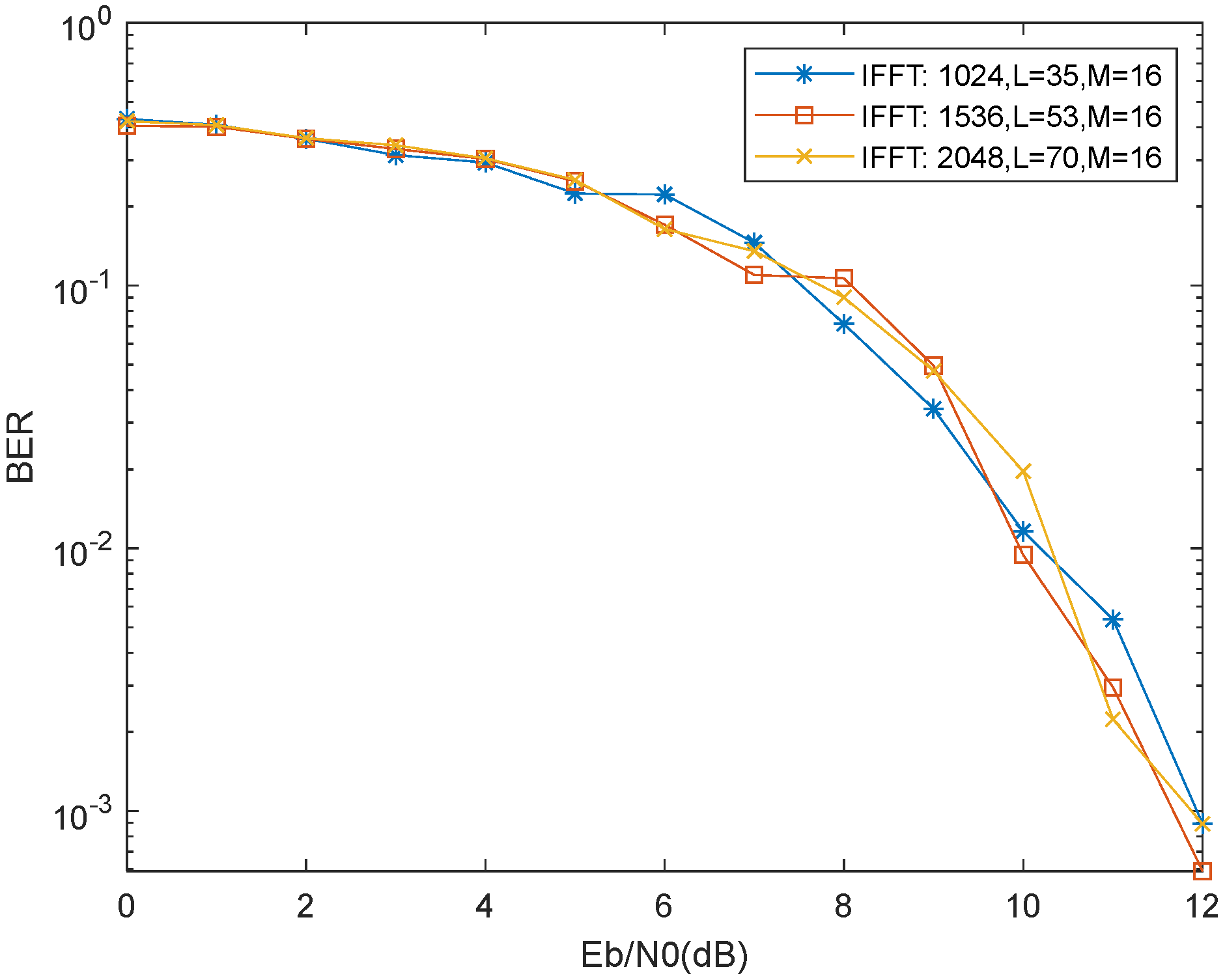
4.1. Influence of IFFT Points on System Performance

According to the 3GPP LTE technical report, the number of IFFT points changes and the number of subcarriers N s u b changes, as shown in Table 1. The number of IFFT points is set to 1024, 1536, and 2048, respectively, and the number of subcarriers in each group M is kept unchanged, so as to change the number of packets L. The 2DLogistic map is used to obtain the experimental data.
Figure 8 shows the impact of different packet numbers on the MC−ODBR−DCSK system using a 2D-Logistic map with initial values of 0.40 and a semi−spread spectrum factor of 100. From the figure above, it can be found that changing the number of IFFT points in the experiment, that is, changing the number of groups L, has little impact on the system bit error performance.

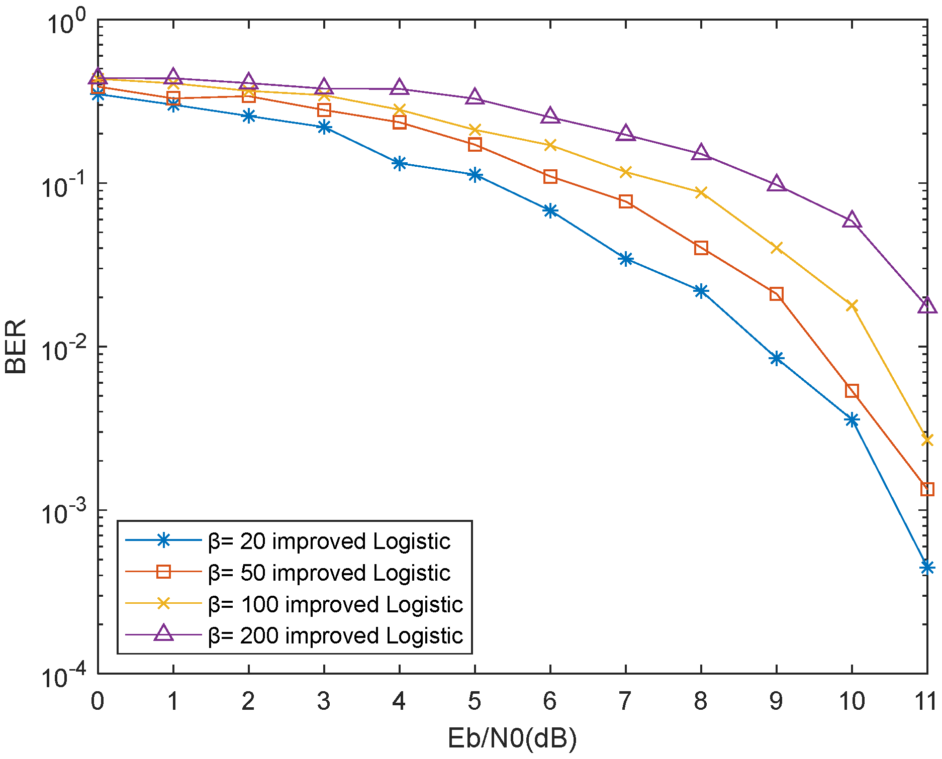
4.2. Influence of Different Chaotic Maps on Performance

Set the same initial value and semi−spread spectrum factor and use different chaotic map equations to explore the influence of different maps on the MC−ODBR−DCSK system. Combined with the map balance degree, the special initial value is avoided when determining the initial value. The following experimental results are representative experimental results selected after multiple adjustments of experimental data. The experiment is performed at semi−spread spectrum factor β = 100 and β = 200, respectively. The simulation results obtained are shown in Figure 9.
After many experimental observations and summaries, the following conclusions can be drawn: under the same initial value conditions, the bit error rate changes of the MC−ODBR−DCSK system generated by different maps under the same semi−spread spectrum factor show a consistent change rule.

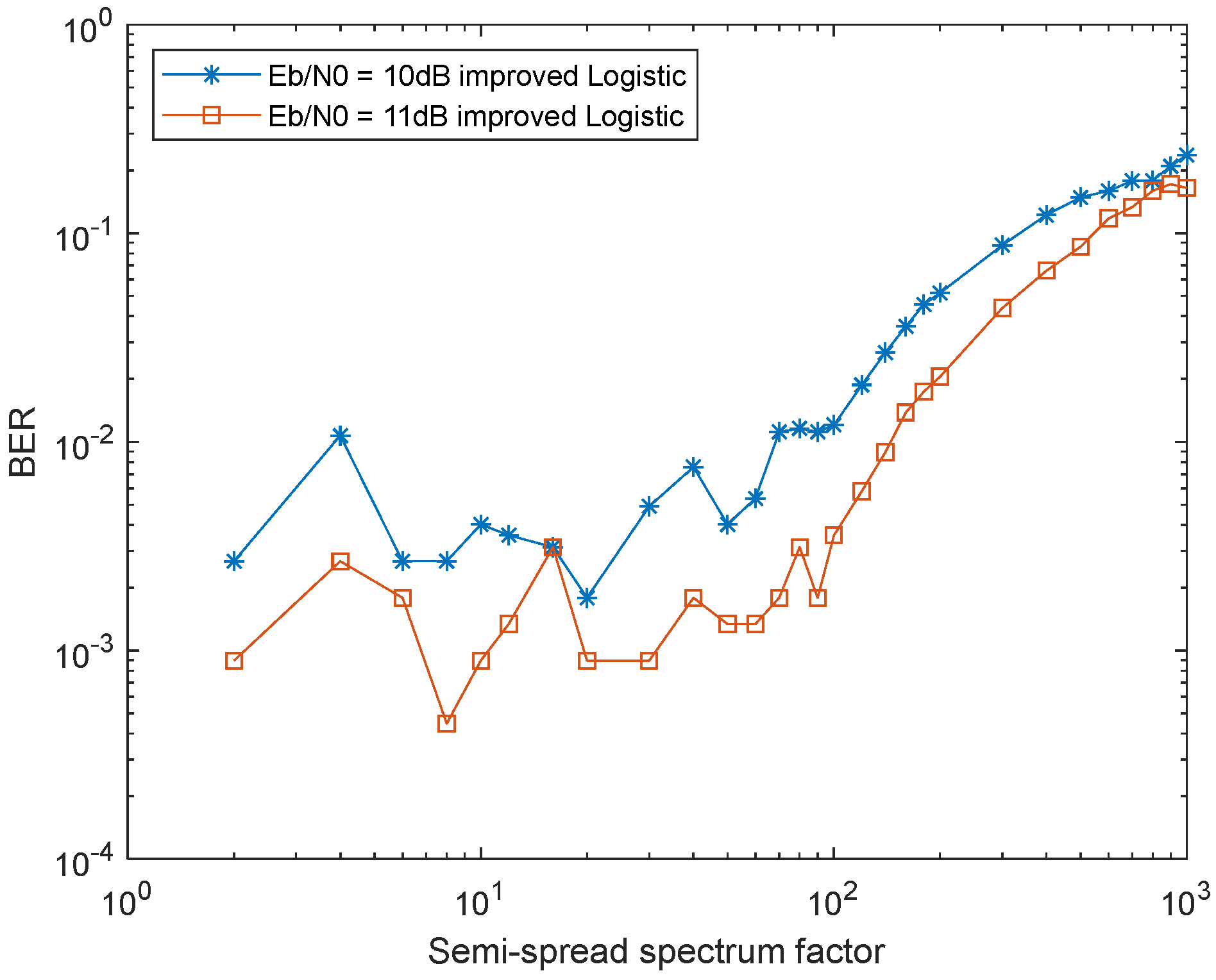
4.3. Influence of Semi−Spread Spectrum Factor on Performance

Using an improved Logistic map with an initial value of 0.40, we selected 20, 50, 100, and 200 semi−spread spectrum factors for simulation experiments. From the simulation results in Figure 10, it can be concluded that selecting different semi−spread spectrum factors will have different effects on the system. Through simulation, it can be seen that the smaller the semi spread spectrum factor, the better the bit error performance of the system. With the increase of the semi-spread spectrum factor, the bit error performance of the system also increases.
The correlation characteristics of the sequence will affect the bit error performance of the system during demodulation. With the increase of the spread spectrum factor, the sequence correlation characteristics become better and better. At the same time, with the increase of the semi-spread spectrum factor, the noise introduced is also increasing. There is a balance point between these two influencing factors, and this balance point is the optimal semi−spread spectrum factor value.
The optimal spread factor of the MC−ODBR−DCSK system is simulated. The experiment, results of which are shown in Figure 11, is to use an improved Logistic map at the SNR of 10 dB and 11 dB to carry out the BER performance curve with semi−spread spectrum factor transformation. With the increase of the spreading factor, the BER performance of different chaotic maps changes gently at first and then becomes worse. Different chaotic maps are applied to the MC−ODBR−DCSK system with different optimal spreading factors.

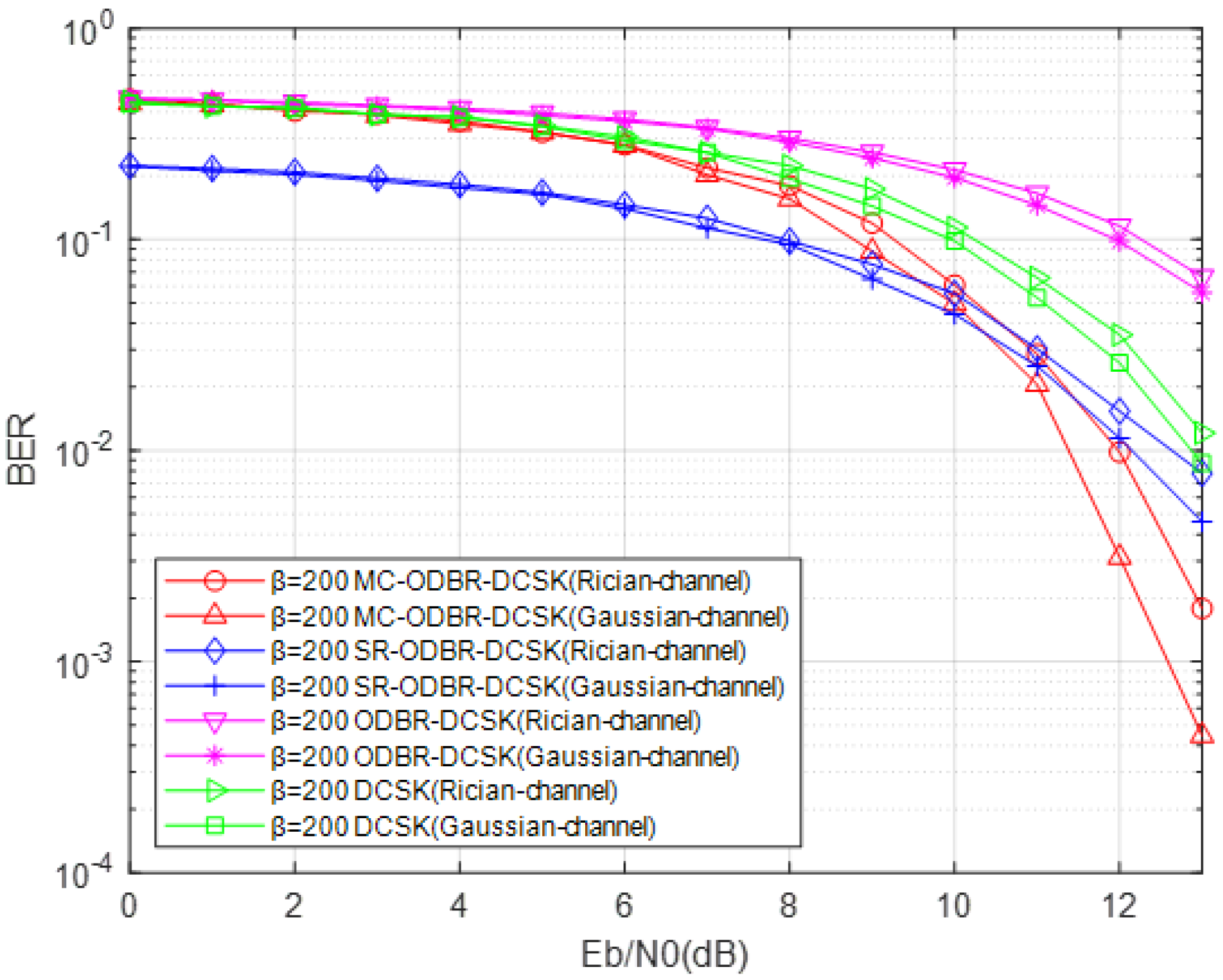
4.4. Bit Error Rate Comparison of Different Systems

Figure 12 illustrates the relationship between the error rates of the MC−ODBR−DCSK, SR−ODBR−DCSK, ODBR−DCSK, and DCSK systems under the same testing conditions. The systems were evaluated using an improved Logistic map and a semi-spread spectrum factor of 200. Based on the experimental results, the SR−ODBR−DCSK system exhibited the best error rate performance when the signal-to-noise ratio (SNR) was less than 11 dB, while the MC−ODBR−DCSK system demonstrated the best error rate performance when the SNR was greater than 11 dB.
Figure 13 depicts the correlation between the number of semi−spread spectrum factors and the bit error rate of four systems, namely MC−ODBR−DCSK, SR−ODBR−DCSK, ODBR−DCSK, and DCSK, when the signal-to-noise ratio is 10 dB in an AWGN channel using the 2D-Logistic map. Generally, as the semi-spread spectrum factor increases, the error rate performance of the MC−ODBR−DCSK system changes slowly at first and then gradually deteriorates. The error rate performance of the SR−ODBR−DCSK system, ODBR−DCSK system, and DCSK system initially increases and then decreases.

5. Conclusions

This paper proposes and analyzes a new MC−ODBR−DCSK system and deduces its energy efficiency. Simulation results show that this system has better energy efficiency compared to MC−DCSK and DCSK systems, using multicarrier transmissions and two orthogonal reference chaotic signal modulations to achieve higher data rates. In addition, when the chaotic signal and the number of packets change, the bit error rate performance hardly changes. Therefore, the system has good confidentiality. Currently, we have studied the software simulation of the MC−ODBR−DCSK scheme, and in the future, we hope to implement the work of chaotic communication signal generation and modulation schemes using a Software Radio Platform based on High−Performance USRP. The MC−ODBR−DCSK system is promising and demonstrates great potential for the future of high-data-rate communication systems.

Author Contributions

Conceptualization, Y.F.; data curation, X.L.; investigation, Q.J.; methodology, T.S.; writing—original draft, B.Q. and F.L. All authors have read and agreed to the published version of the manuscript.

Funding

This work is supported in part by the National Natural Science Foundation of China (Grant No. 61971291), the central government leading local science and technology development projects (2022020128-JH6/1001), Shenyang Natural Science Foundation (Grant No. 22-315-6-10), and the science and technology funds from Liaoning Education Department (serial number: LJKZ0242).

Conflicts of Interest

The authors declare no conflict of interest.

References

  1. Kaddom, G.; Tadayon, N. Differential chaos shift keying: A robust Modulation Scheme for Power-Line Communications. IEEE Trans. Circuits Syst. II Express Briefs 2017, 64, 31–35. [Google Scholar] [CrossRef] [Green Version]
  2. Xu, W.-K.; Wang, L.; Kolumbán, G. A novel differential chaos shift keying modulation scheme. Int. J. Bifurc. Chaos 2011, 21, 799–814. [Google Scholar] [CrossRef]
  3. Kaddom, G.; Soujeri, E. NR-DCSK: A Noise Reduction Differential Chaos Shift Keying System. IEEE Trans. Circuits Syst. II Express Briefs 2016, 63, 648–652. [Google Scholar] [CrossRef] [Green Version]
  4. Hu, W.; Wang, L.; Kaddom, G. Design and performance analysis of a differentially spatial modulated chaos shift keying modulation system. IEEE Trans. Circuits Syst. Ⅱ Express Briefs 2017, 64, 1302–1306. [Google Scholar] [CrossRef]
  5. Liu, F.; Feng, Y.-X. Dynamic Multimapping Composite Chaotic Sequence Generator Algorithm. Int. J. Electron. Commun. 2019, 107, 231–238. [Google Scholar] [CrossRef]
  6. Zhang, M.; Cheng, G.; Yang, B.; Yang, C. Generalized Carrier Index Differential Chaos Shift Keying Based SWIPT with Conversion Noise and Path Loss-Effect. Electronics 2022, 11, 2406. [Google Scholar] [CrossRef]
  7. Jia, Y.-Q.; Jiang, G.-P.; Yang, H.; Yu, B.; Du, M.-D. Design and Performance Analysis of a Multi-Carrier M−Ary DCSK System with Multilevel Code-Shifted Modulation Based on Fractional−Order Chaos. Electronics 2021, 10, 2343. [Google Scholar] [CrossRef]
  8. Yang, H.; Jiang, G.-P. High-efficiency differential−chaos−shift−keying scheme for chaos−based noncoherent communication. IEEE Trans. Circuits Syst. II Express Briefs 2012, 59, 312–316. [Google Scholar] [CrossRef]
  9. Kaddoum, G.; Soujeri, E.; Arcila, C.; Eshteiwi, K. I−DCSK: An improved non-coherent communication system architecture. IEEE Trans. Circuits Syst. II Express Briefs 2015, 62, 901–905. [Google Scholar]
  10. Zhang, L.; Zhang, H.; Jiang, Y.; Wu, Z. Intelligent and reliable deep learning LSTM neural networks-based OFDM−DCSK demodulation design. IEEE Trans. Veh. Technol. 2020, 69, 16163–16167. [Google Scholar] [CrossRef]
  11. Qiu, W.; Yang, Y.; Feng, Y.; Zhang, L.; Wu, Z. Secure MIMO Communication System with Frequency Hopping Aided OFDM-DCSK Modulation. Electronics 2022, 11, 3029. [Google Scholar] [CrossRef]
  12. Kaddoum, G. Design and performance analysis of a multi-user OFDM based differential chaos shift keying communication system. IEEE Trans. Commun. 2016, 64, 249–260. [Google Scholar] [CrossRef] [Green Version]
  13. Kaddoum, G.; Soujeri, E.; Nijsure, Y. Design of a Short Reference Noncoherent Chaos−Based Communication Systems. IEEE Trans. Commun. 2016, 64, 680–689. [Google Scholar] [CrossRef] [Green Version]
  14. Kaddoum, G.; Tran, H.-V.; Kong, L.; Atallah, M. Design of Simultaneous Wireless Information and Power Transfer Scheme for Short Reference DCSK Communication Systems. IEEE Trans. Commun. 2017, 65, 431–443. [Google Scholar] [CrossRef]
  15. Sui, T.; Feng, Y.-X.; Jiang, Q.; Liu, F.; Zhang, T. Design and Analysis of a Short Reference Orthogonal Double Bit Rate Differential Chaotic Shift Keying Communication Scheme. Electronics 2022, 11, 2020. [Google Scholar] [CrossRef]
  16. Kaddoum, G.; Gagnon, F.; Richardson, F.-D. Design of a secure Multi-Carrier DCSK system. In Proceedings of the 2012 International Symposium on Wireless Communication Systems (ISWCS), Paris, France, 28–31 August 2012; pp. 964–968. [Google Scholar]
  17. Liu, Z.-F.; Zhang, L.; Wu, Z.-Q.; Bian, J. A secure and robust frequency and time diversity aided OFDM-DCSK modulation system not requiring channel state information. IEEE Trans. Commun. 2020, 68, 1684–1697. [Google Scholar] [CrossRef]
  18. Kaddoum, G.; Richardson, F.-D.; Gagnon, F. Design and analysis of a Multi−Carrier differential chaos shift keying communication system. IEEE Trans. Commun. 2013, 61, 3281–3291. [Google Scholar] [CrossRef] [Green Version]
  19. Yang, H.; Tang, W.-K.-S.; Chen, G.-R.; Jiang, G.-P. Multi−Carrier Chaos Shift Keying: System Design and Performance Analysis. IEEE Trans. Circuits Syst. I Regul. Pap. 2017, 64, 2182–2194. [Google Scholar] [CrossRef]
  20. Huang, T.-T.; Wang, L.; Xu, W.-K.; Chen, G. A multi−carrier M−ary differential chaos shift keying system with low PAPR. IEEE Access 2017, 5, 18793–18803. [Google Scholar] [CrossRef]
  21. Kaddoum, G.; Shokraneh, F. Analog network coding for multi−user multi−carrier differential chaos shift keying communication system. IEEE Trans. Wirel. Commun. 2015, 14, 1492–1505. [Google Scholar] [CrossRef]
  22. Chen, Z.-W.; Zhang, L.; Wu, Z.-Q.; Wang, L.; Xu, W. Reliable and efficient sparse code spreading aided MC−DCSK transceiver design for multiuser transmissions. IEEE Trans. Commun. 2021, 69, 1480–1495. [Google Scholar] [CrossRef]
  23. Chen, M.-L.; Xu, W.-K.; Wang, D.-Q.; Wang, L. Multi−carrier chaotic communication scheme for underwater acoustic communications. IET Commun. 2019, 13, 2097–2105. [Google Scholar] [CrossRef]
  24. Zhang, G.; Zhao, C.; Zhang, T. Performance Analysis of MISO−MU−OHE−DCSK System over Rayleigh Fading Channels. AEU Int. J. Electron. Commun. 2019, 115, 153048. [Google Scholar] [CrossRef]
Figure 1. Time domain diagram. (a) Improved Logistic Map ( x 0 = 0.40 , μ = 2); (b) 2D-Logistic map ( x 0 = 0.40 , y 0 = 0.40 , r = 1.19).
Electronics 12 01785 g001
Figure 2. Block diagram of OCG.
Electronics 12 01785 g002
Figure 3. Transmitter of MC-ODBR-DCSK.
Electronics 12 01785 g003
Figure 4. The signal structure of MC−ODBR−DCSK.
Electronics 12 01785 g004
Figure 5. Format of the signal transmitted in the MC−ODBR−DCSK system.
Electronics 12 01785 g005
Figure 6. Receiver of MC−ODBR−DCSK.
Electronics 12 01785 g006
Figure 7. Comparison of DBR of data subcarriers in different systems.
Electronics 12 01785 g007
Figure 8. BER performance curves of the system with different number of IFFT points.
Electronics 12 01785 g008
Figure 9. BER curves of the system with different chaos maps. (a) β = 100, x0 = 0.40; (b) β = 200, x0 = 0.40.
Electronics 12 01785 g009
Figure 10. BER curves of the system with different semi−spread spectrum factors.
Electronics 12 01785 g010
Figure 11. Relationship between semi−spread spectrum factor and bit error rate.
Electronics 12 01785 g011
Figure 12. Comparison of bit error rates of DCSK, ODBR−DCSK, SR−ODBR−DCSK, and MC−ODBR-DCSK systems in Gaussian and Rician channels.
Electronics 12 01785 g012
Figure 13. Relationship between semi−spread spectrum factor and bit error rate in Gaussian channel.
Electronics 12 01785 g013
Table 1. Some simulation parameters.
Bandwidth
(MHz)
IFFT Points N s u b N d a t a N p i l o t
10102459556035
15153690184853
2020481190112070
Disclaimer/Publisher’s Note: The statements, opinions and data contained in all publications are solely those of the individual author(s) and contributor(s) and not of MDPI and/or the editor(s). MDPI and/or the editor(s) disclaim responsibility for any injury to people or property resulting from any ideas, methods, instructions or products referred to in the content.

