Article

A Three-Step Tapered Bit Period SAR ADC Using Area-Efficient Clock Generation

School of Electrical Engineering and Computer Science, Gwangju Institute of Science and Technology, Gwangju 61005, Republic of Korea
*
Author to whom correspondence should be addressed.
Electronics 2023, 12(8), 1863; https://doi.org/10.3390/electronics12081863
Submission received: 8 March 2023 / Revised: 6 April 2023 / Accepted: 13 April 2023 / Published: 14 April 2023
(This article belongs to the Special Issue CMOS Integrated Circuits Design)

Abstract

:
A three-step tapered bit period asynchronous successive approximation register (SAR) analog-to-digital converter (ADC) is proposed to reduce the total DAC settling time by 47.7% compared to the non-tapered conversion time with less design overhead. Unlike conventional approaches, the SAR settling time analysis with both reference buffer output impedance and hardware overhead is first analyzed in each conversion step, which demonstrates that the three-step tapered bit period approach is the most time- and hardware efficient in our design. Additionally, area-efficient three-step clock generation is proposed by sharing resistors for delay generation, resulting in a small area increase of only 20.4% compared to the non-tapered clock generation. As a result, the proposed technique is used to reduce the reference buffer’s power and increase the sampling frequency. The maximum allowed output impedance of the reference buffer for SFDR > 92 dB becomes larger than that of the non-tapered design by 200 Ω , translated to a sampling frequency increase from 6 MHz to 8 MHz in our design. The proposed three-step tapered bit period using an area-efficient clock generator was designed in a 55 nm CMOS process. The clock generator occupies 0.00081 mm 2 out of 1143 μ m × 81 μ m overall size. The power consumption of the 8 MS/s 12-bit SAR ADC with proposed clock generation is 128.91 μ W when under 1 V supply.

1. Introduction

Due to the growing prevalence of IoT devices, power-efficient successive approximation register (SAR) analog-to-digital converters (ADCs) are now widely utilized in various fields, including sensor networks, wearable devices, and biomedical applications, where low power consumption is essential [1,2,3,4,5,6,7,8]. For a high sampling rate as well as low power consumption, various research studies are being conducted to reduce the waste of time in conversion time [9,10,11,12,13,14,15]. Asynchronous SAR ADC requires a conversion clock generation circuit for a comparator and capacitive digital–analog converter (CDAC), as shown in Figure 1 [16]. After the comparator decision, comparator clock generation (COMP CLK GEN) generates a delay time in the conversion cycle for CDAC settling. However, there is a waste of time in the conventional method, where the maximum DAC settling time for MSB is reused in other LSB conversions, although the required settling time is relaxed in LSB conversions. A two-step delay technique in high-resolution ADC [17] is proposed instead of utilizing different optimized delays in all conversion cycles for less hardware overhead. In addition, an all-tapered delay technique in mid-resolution ADC is proposed in [18] to reduce the conversion time even further. The previous works [17,18] studied the effect of the DAC switch but did not consider the impedance of the reference that is also a significant factor in determining the DAC settling time [19]. In this paper, we analyze the effect of both reference and switch impedances and find that a tapering conversion of more than three becomes inefficient considering the hardware overhead. If the reference buffer’s impedance is considered, the required settling time from MSB down to the LSB conversion cycle is reduced exponentially, unlike the linear decrease that is observed when only the switch impedance is considered. Therefore, a three-step tapered bit period method is implemented to minimize the complexity of circuit implementation and reduce the waste of conversion time more efficiently. The post-layout simulation confirms that the sampling speed is increased by 33.3% and the power of the reference buffer reduces to half in our 12-bit SAR ADC.
The composition of this paper is as follows. We analyze the settling time of the CDAC when considering the reference buffer and the clock generation method with the most efficient number of delays in Section 2. In addition, we propose a circuit implementation method in Section 3 that shares resistance to minimize areas and reduce complexity. Section 4 shows the post-simulation result that increases the sampling rate under the limited DAC settling conditions or reduces the power of the reference buffer by using a three-step tapered delay. Finally, we conclude this brief in Section 5.

2. Analysis of Capacitive DAC Settling

2.1. Equation of Required CDAC Settling Time with Reference Buffer

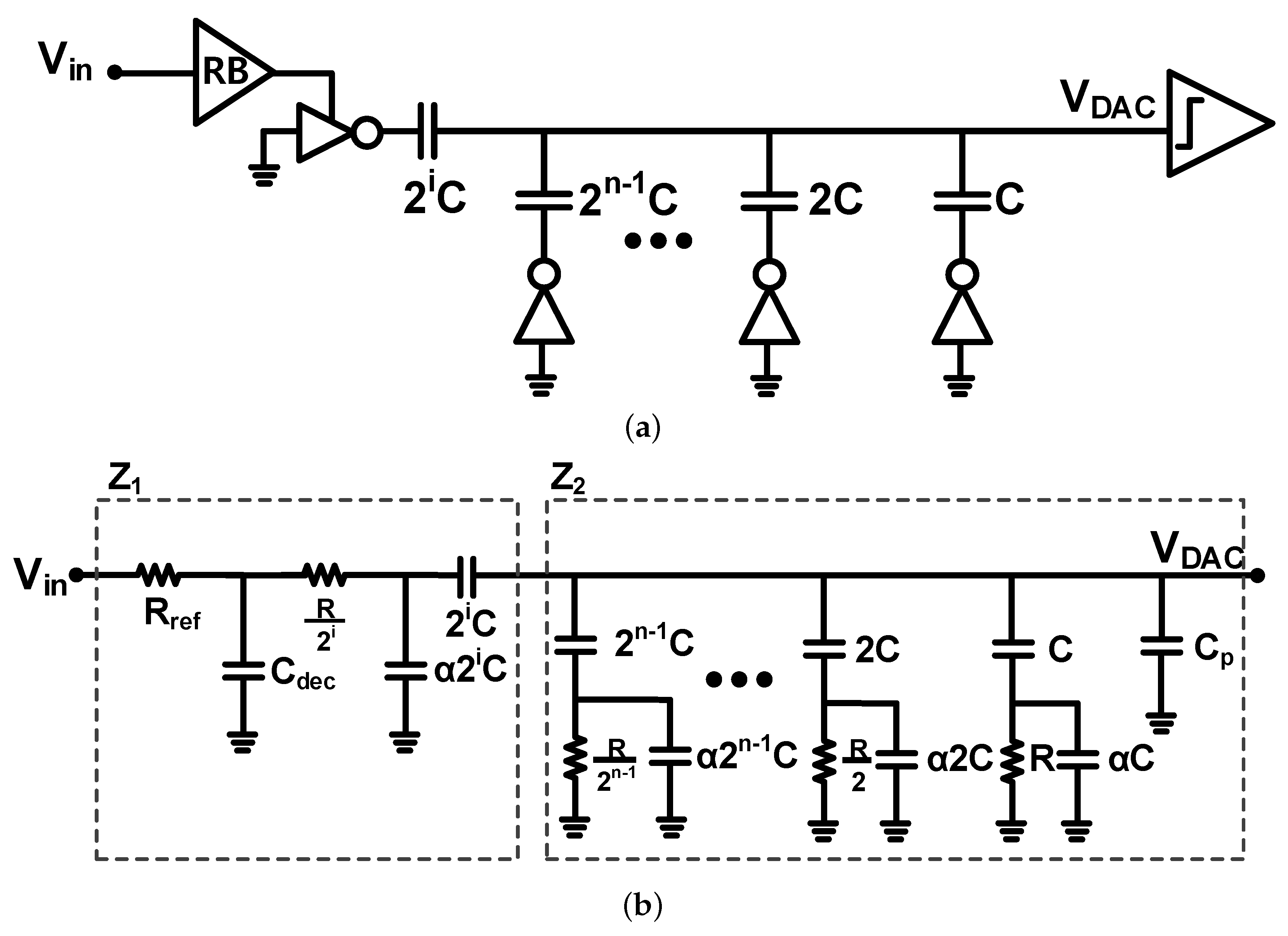
In order to derive the most efficient tapered clock generation scheme, the required DAC settling time is found in each conversion cycle by finding the transfer function from the reference buffer to the comparator input node. A top-plate sampling CDAC is used with a boot-strapped track and hold circuit as shown in [20]. Figure 2a shows an equivalent n-bit CDAC array model when using a monotonic switch scheme [20], including DAC switches, a reference buffer (RB), and parasitic effects. The output impedance of the reference buffer is denoted as R r e f , and C d e c is the capacitor used for noise filtering. In addition, the resistance size of the CDAC switch is R, and the parasitic capacitance factor in the DAC switch is α . In the capacitive DAC array, the unit capacitor is C, and the ith CDAC capacitor is 2 i C , where i ranges from 0 to n 1 . We use a monotonic switching method, so an n-bit CDAC constitutes an ( n + 1 ) -bit SAR ADC [20]. Using this model, the required settling time from the reference buffer to V D A C in the ith conversion cycle is calculated as follows:
V D A C ( s ) = Z 2 Z 1 + Z 2 · V i n
H ( s ) = V D A C ( s ) V i n = X ( s ) s 2 i R r e f C ( 1 + α + α X ( s ) ) + ( 1 + s C d e c R r e f ) ( 1 + X ( s ) + s R C ( 1 + α + α X ( s ) ) )
w h e r e X ( s ) = 2 i C ( 1 + s R C + s α R C ) ( 2 n C 2 i C ) ( 1 + s α R C ) + s R C C p ( 1 + α ) + C p
To simplify the transfer function, some factors are substituted for X ( s ) . In order to calculate the required CDAC settling time, the transient step response is found by the inverse Laplace transform with a step input:
V D A C ( t ) = L 1 H ( s ) · V r e f · 1 s
The settling error in the ith conversion is found as shown below:
V e r r o r ( t ) = 2 i C 2 n C + C p V D A C ( t )
The required settling time to make the error less than half LSB ( V r e f 2 · ( 2 n + C p C ) ) is found by the numerical computation. In addition, we assume that n is 11, R is 6 k Ω , C p is 1.2 pF, V r e f is 1 V, C d e c is 500 fF and α is 1.7. In order to ensure that the KT/C noise is below 1/4 LSB and to consider the settling time of the CDAC, C is 1 fF in our 12-bit SAR ADC. Therefore, Figure 3 shows the required time in the ith conversion cycle for three reference buffer resistances ( R r e f = 0, 200, 400 Ω ). It is noted that for R r e f = 0, the required settling time decreases linearly from the MSB (i = 10) to the LSB. However, for higher R r e f cases, the required settling time exponentially decreases going down to the LSB conversion. Recent studies proposed a two-step delay technique [17] and an all-tapered delay technique [18] but neither proposed the impedance of R r e f . According to Equations (2)–(4), increasing the resistance value leads to an increase in settling time. If the settling time exceeds the given time, decision errors occur, which result in degraded linearity. Therefore, to decide on a proper clock tapering scheme, R r e f impedance must also be considered.
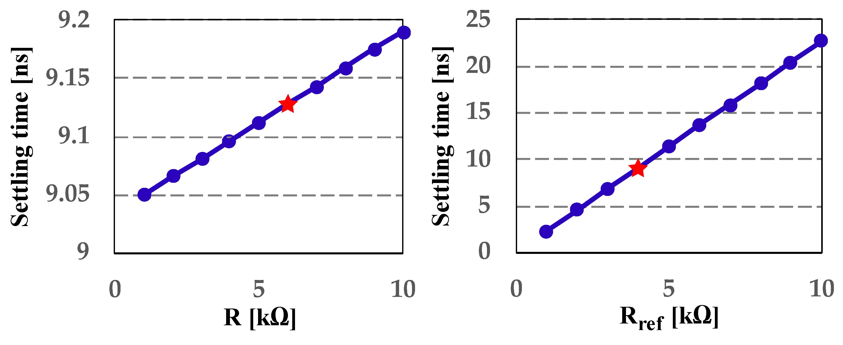
According to Equation (3), the two resistive factors that affect the settling time are R r e f and R for the given CDAC. The effect of the resistive factors is found by sweeping the variables around the design point marked with star, as shown in Figure 4. The size of R r e f is a dominant factor to determine the required settling time because the DAC buffer is scaled and the switch resistance R is also scaled accordingly; however, the R r e f is common for all conversions. Considering R r e f , in order to find efficient tapered delay steps, multiple tapering scenarios are simulated for different R r e f impedances.

2.2. Analysis of Conversion Time According to Various Techniques

Table 1 shows the minimum required total conversion time according to various tapering techniques. The most conventional technique is a non-tapered technique with a single delay, which uses the required settling time of MSB as the worst delay. Therefore, the minimum required total conversion time for the non-tapered technique is n times the required settling time of the MSB. According to the size of each R r e f , Table 1 defines the non-tapered technique as 100% and compares it with other techniques with various delays. Above all, all-tapered is the ideal case assuming that the designer can create an accurate delay calculated by Equation (4) so that the settling error in each conversion becomes below half LSB and the wasted time is zero. However, generating an accurate delay is almost impossible due to the effects of PVT variation and hardware overhead. Especially for a wide range of delay generation, the minimum delay is typically limited by the trade-off between the range and resolution for the given number of digital control bits. So, the achievable minimum delay is limited to 2.3 ns in our design. For this reason, l i m i t e d   all-tapered reflects the minimum delay that can be used for tapering. Therefore, the faster reference settling by smaller R r e f requires a finer LSB delay step that is difficult to be implemented in the l i m i t e d   all-tapered case. Thus, the difference between all-tapered and l i m i t e d   all-tapered becomes smaller as R r e f increases, where the required delay step in LSBs can be easily generated in our circuit. Considering minimum clock delay generation, the achievable minimum delay by all tapering is limited to l i m i t e d   all-tapered . To determine the optimal number of tapering steps, the values from l i m i t e d   all-tapered are compared with several other tapering levels.
In order to find the minimum total conversion time in two to four tapering levels, the minimum conversion cycle time is assumed to start at 2.3 ns with a step of 100 ps, and the rest of the tapering period scales with a step of 0.05 by a scaling factor (weight) according to Equation (5). The tapering clock position is then swept across all possible combinations to find the best delay transition for tapering in a 12-bit ADC:
d e l a y [ k ] = d e l a y [ k 1 ] w e i g h t [ k 1 ] , k { 2 , , n u m b e r o f d e l a y }
Each simulation is performed under different R r e f conditions, as shown in Table 1. Using a two-step technique reduces the minimum required total conversion time by 51.87% on average compared to the non-tapered technique, and using a three-step technique reduces it by 58.07%, on average. However, the difference between three-step and four-step is less than 1% when R r e f is over 400 Ω . When R r e f is less than 300 Ω and the minimum delay is limited to 2.3 ns, tapering more than four-step is unnecessary because the minimum total conversion time exceeds that of non-tapering. If we can further reduce the minimum delay below 2.3 ns, the required total conversion time may reduce, but the hardware overhead may increase. Moreover, the difference between l i m i t e d   all-tapered and three-step is within 5% for all R r e f cases. For this reason, we adopted the three-step tapered bit period delays, which most effectively reduces the required settling time and the overhead of circuit implementation.
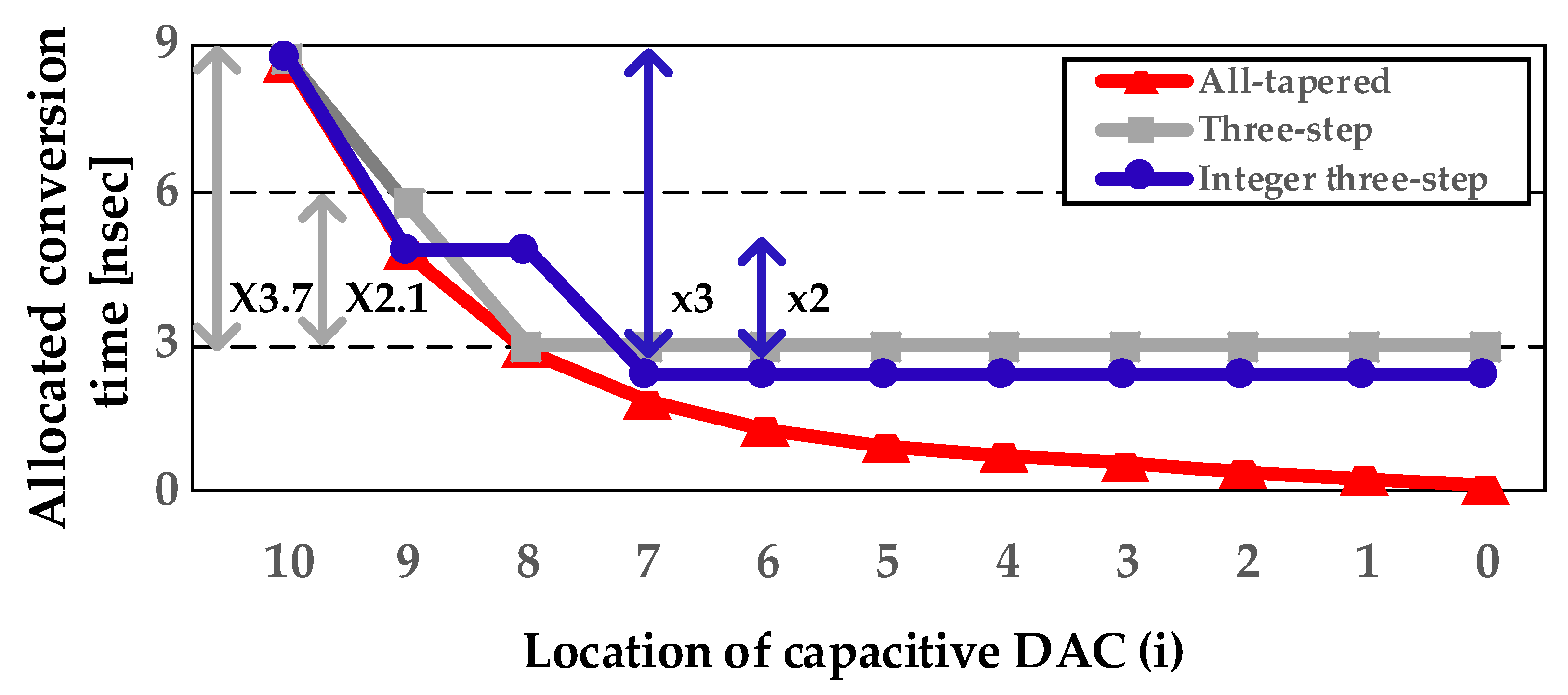
To implement the three-step tapered technique, we determine the optimal weights using a simple implementation independent of R r e f size. As a result, we adopt the i n t e g e r   three-step method, which uses three delay steps scaled by integer multiples of 1, 2, and 3. I n t e g e r   three-step is the simplest to implement but reduces conversion time by 48.08% on average compared to non-tapered . In particular, the total conversion time difference between the three-step and i n t e g e r   three-step methods is only 3.85 ns when R r e f is 400 Ω , which is our design point. Additionally, the Figure 5 compares the allocated conversion times in each conversion step for the all-tapered , three-step and i n t e g e r   three-step techniques according to the location of the CDAC, where R r e f = 400 Ω . The most efficient delay configuration for the three-step technique is to use a delay of 8.694 ns once for the MSB, a delay of 4.83 ns twice for MSB-1, MSB-2, and a delay of 2.3 ns for each of the eight CDACs starting from the LSB. As a result, the three-step technique utilizes fractional values (multiplied by 2.1 and 3.7, when Rref = 400 Ω ) to calculate delay times for unconstrained weights. However, fractional values are different according to the size of R r e f , and implementing such fractional values in hardware can be challenging. The i n t e g e r   three-step technique provides a simpler alternative by multiplying the least significant bit (LSB) delay time (2.3 ns) by integer values of 2 and 3, resulting in a negligible increase in the total conversion time. To implement the i n t e g e r   three-step   t e c h n i q u e , an integer multiple delay cell can generate the clock signal needed for the conversion process. This approach simplifies the hardware implementation of the technique and helps reduce conversion time without compromising conversion accuracy.

3. Proposed Three-Step Tapered Bit Period Clock Generator Circuit Implementation

3.1. Asynchronous SAR Logic

The structure of the comparator clock generator and SAR control logic is depicted in Figure 6a, while the SAR control logic used to control the CDAC sampling switch is shown in Figure 6b [16,20,21]. Moreover, Figure 6c is the timing diagram of the comparator clock generator. The comparator clock generation consists of two paths, the CDAC settling, and the comparator reset paths. The C L K signal serves as the sampling clock, while the C O M P _ C L K controls the comparator. The C O M P _ D O N E signal comes from the comparator as shown in Figure 1. The comparator operates when the C O M P _ C L K becomes high, and C O M P _ D O N E rises after the completion of the comparison. Since the comparator needs to reset, a signal is transmitted in the comparator reset path to reset the C O M P _ C L K . Then, the comparator clock generation operates in the CDAC settling direction, and when the F I N I S H goes low after passing the D E L A Y   C E L L , C O M P _ C L K rises, and the comparator operates again. Furthermore, the SAR control logic generates a C O M P signal whenever the comparison is complete, and a flip-flop in the shift register generates the S T O P signal to indicate the end of the conversion.

3.2. Implementation of Delay Cell and Control Generator

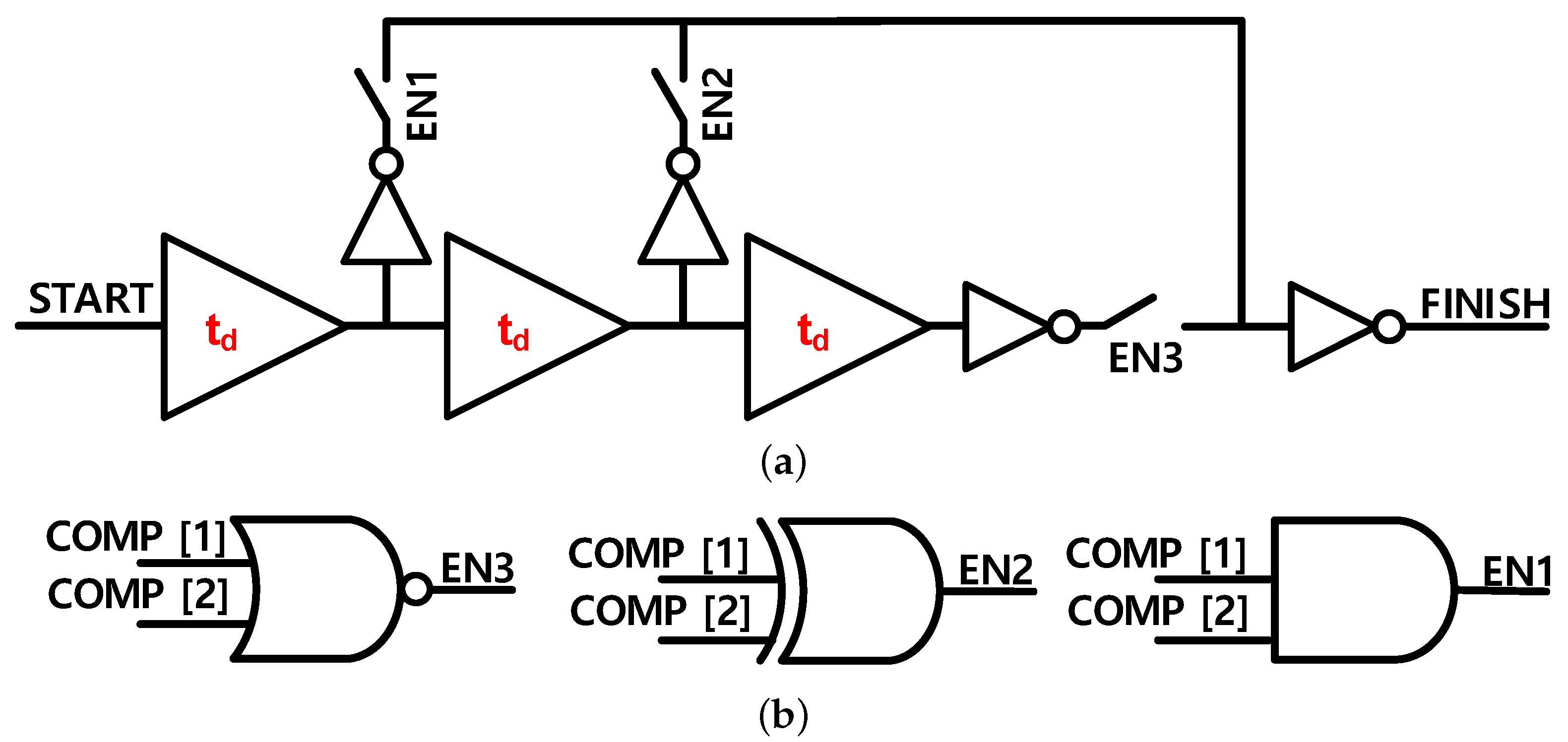
Keeping the designs of the delay cell and control generator simple is essential, even when using tapered techniques. Figure 7a illustrates a conceptual clock generation for three-step tapering, with delays implemented using integer multiples and buffers to reduce circuit complexity. The delay control generator in Figure 7b uses just three logic gates. E N controls the delay time and changes with C O M P signals, as shown in Figure 6c. Note that using three-step tapering delays triples the area of the delay cell. To mitigate this increase, we suggest sharing pull-up ( R u p ) and pull-down ( R d o w n ) resistors, resulting in a more modest 20.4% area increase compared to the three-fold increase seen without this approach.
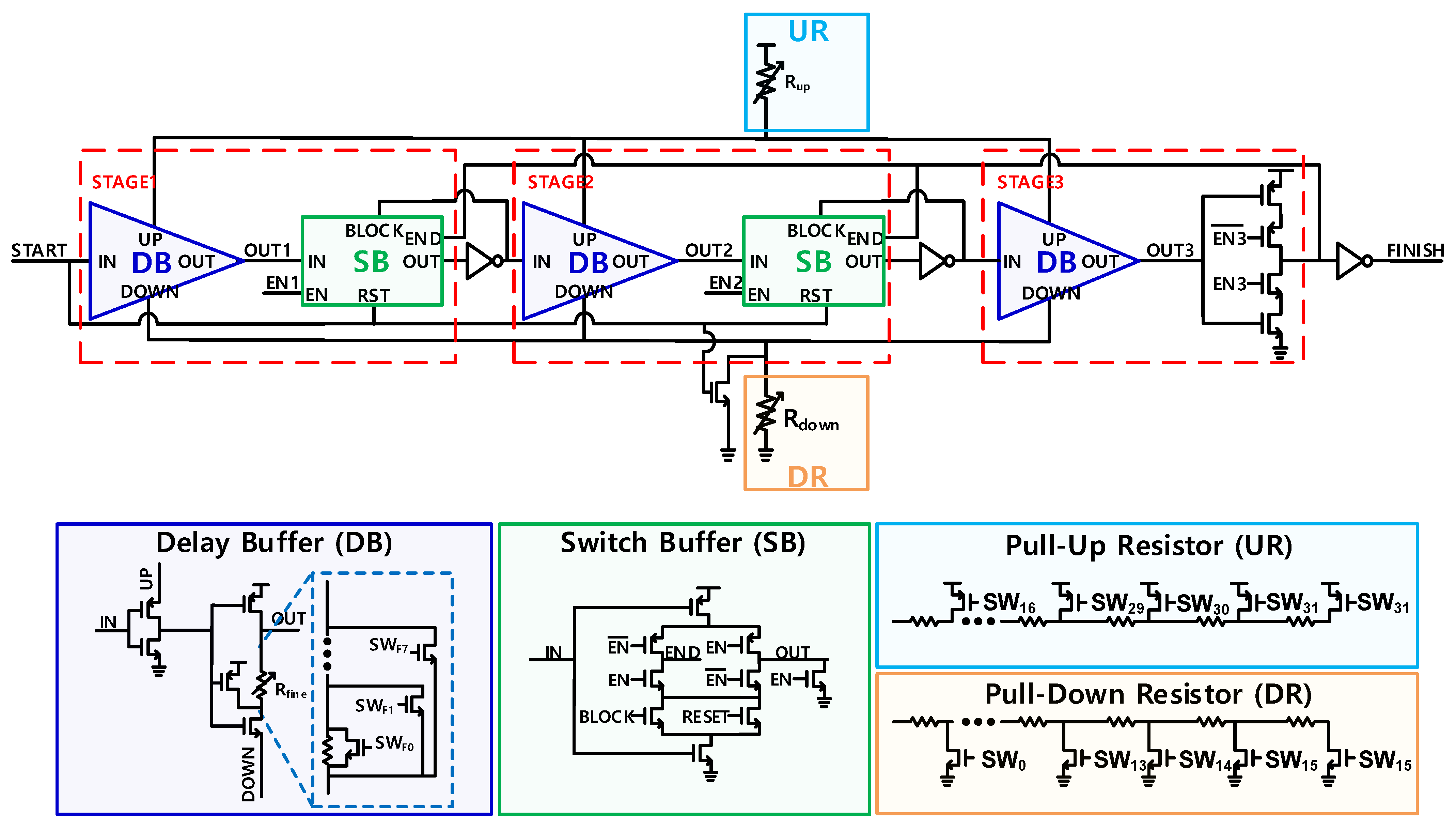
Figure 8 shows the clock generator implementation that scales by integer multiples. The implementation is divided into three stages, each of which contains 256 delays that are determined by the 5-bit coarse and 3-bit fine digital codes. The 5-bit coarse delay controls the size of the common pull-up and pull-down resistors. The 3-bit fine delay code is shared across three buffer blocks. Within each stage, a buffer circuit generates the delay, and a switch circuit controls whether the delay generation should continue or stop. The delay cell is implemented using resistors for energy efficiency, as opposed to other structures, such as the starved structure which incurs energy consumption due to the bias circuit, and the inverter chain structure, which results in dynamic power consumption. The delay cell generates delay time by using a buffer circuit to adjust the rising and falling time of poly resistors connected to the inverter’s supply and ground.
The delay generation starts from the falling edge of the S T A R T signal. Since the first conversion cycle uses the 3 t d mode, E N 3 becomes high and passes through all three stages. In the second conversion cycle, which uses the 2 t d mode, only stage 1 and stage 2 are passed, so the node of O U T 3 does not move. From the third conversion cycle, only stage 1 is passed.
The switches controlled by digital code regulate the delay time. To ensure that the maximum delay time is over 15 ns when using the 3-step tapering technique, the size of the resistors is determined. The pull-up resistor range spans 7.3 k Ω to 175.2 k Ω , with the coarse code step being 7.3 k Ω for codes 17 to 23, and 14.6 k Ω for codes 24 to 31. The pull-down resistor range is from 7.3 k Ω to 58.4 k Ω with a 7.3 k Ω step. When generating the maximum 8 codes with pull-up resistor, the delay time between digital codes decreases due to the charge being pulled from the parasitic capacitor instead of from the supply. To prevent this, the resistor used to generate the maximum 8 coarse codes has a larger value than the other resistors. To ensure that the area efficiency is not compromised when using three-step tapering delays, we propose a coarse resistor-sharing scheme that occupies 64.7% of the total area. This approach results in a modest 20.4% increase in the clock generation area compared to the non-tapered technique.
However, when a delay cell utilizes more than one stage, the shared resistor scheme may result in malfunctions, as shown in Figure 9. The charges in the parasitic capacitor ( C p ) are supposed to be discharged through the R d o w n resistors, but during the discharge of C p , the internal node D O U T experiences a glitch that may trigger the next switch circuit by exceeding the threshold value. To prevent malfunction, we propose a B l o c k signal in the switch circuit where the B l o c k signal becomes ‘0’ after edge propagation finishes.

4. Post-Simulation Result

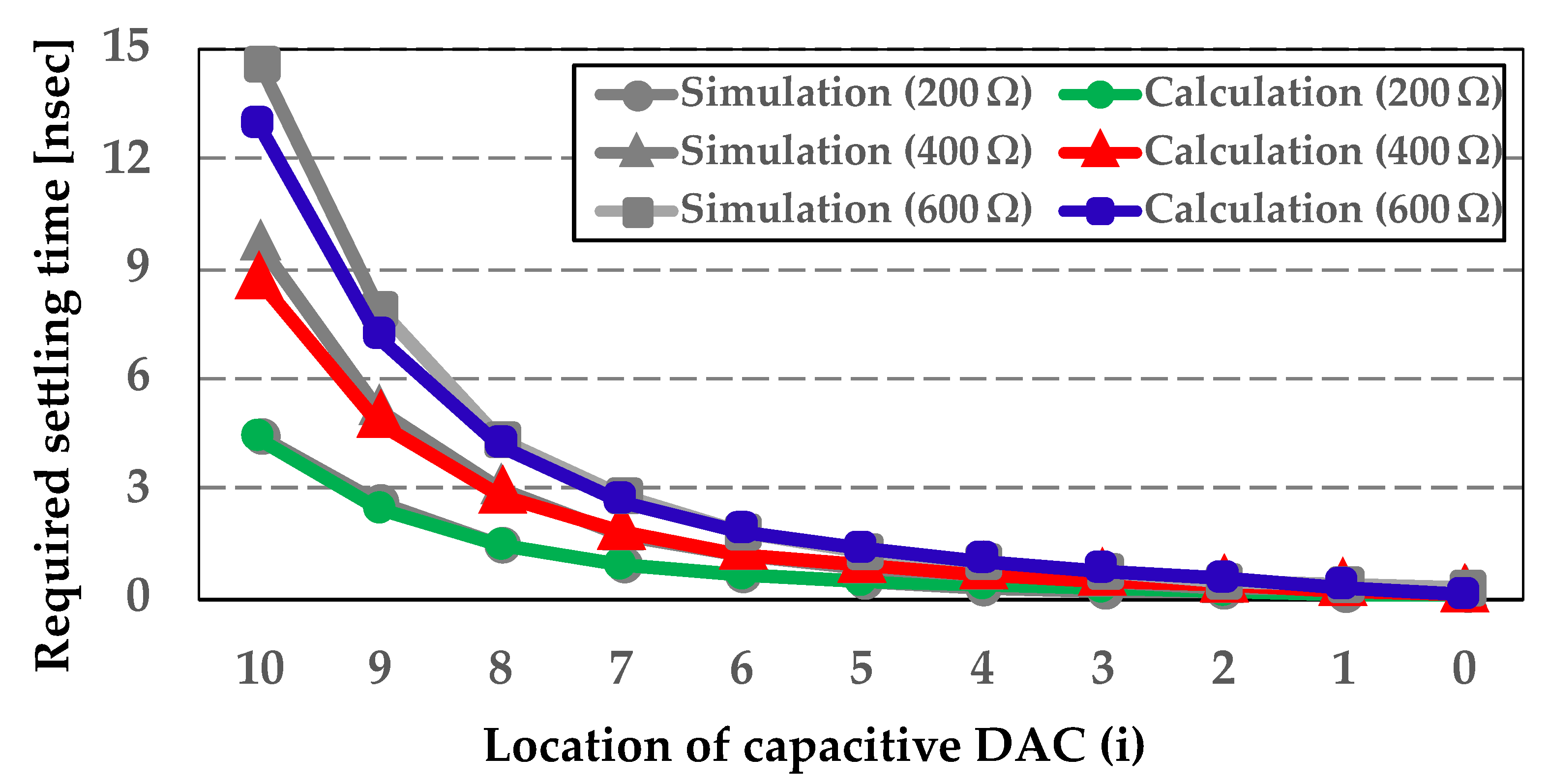
Figure 10 plots the minimum required settling times for less than half of the LSB error according to the location of CDAC and size of the R r e f . Comparing our calculation by Equation (4) and the post-layout simulation result at the nominal corner, the difference between the calculation and the simulation result is less than 18%, except for the two LSBs. Therefore, clock generation using an integer three-step technique is implemented based on an equation with high accuracy.
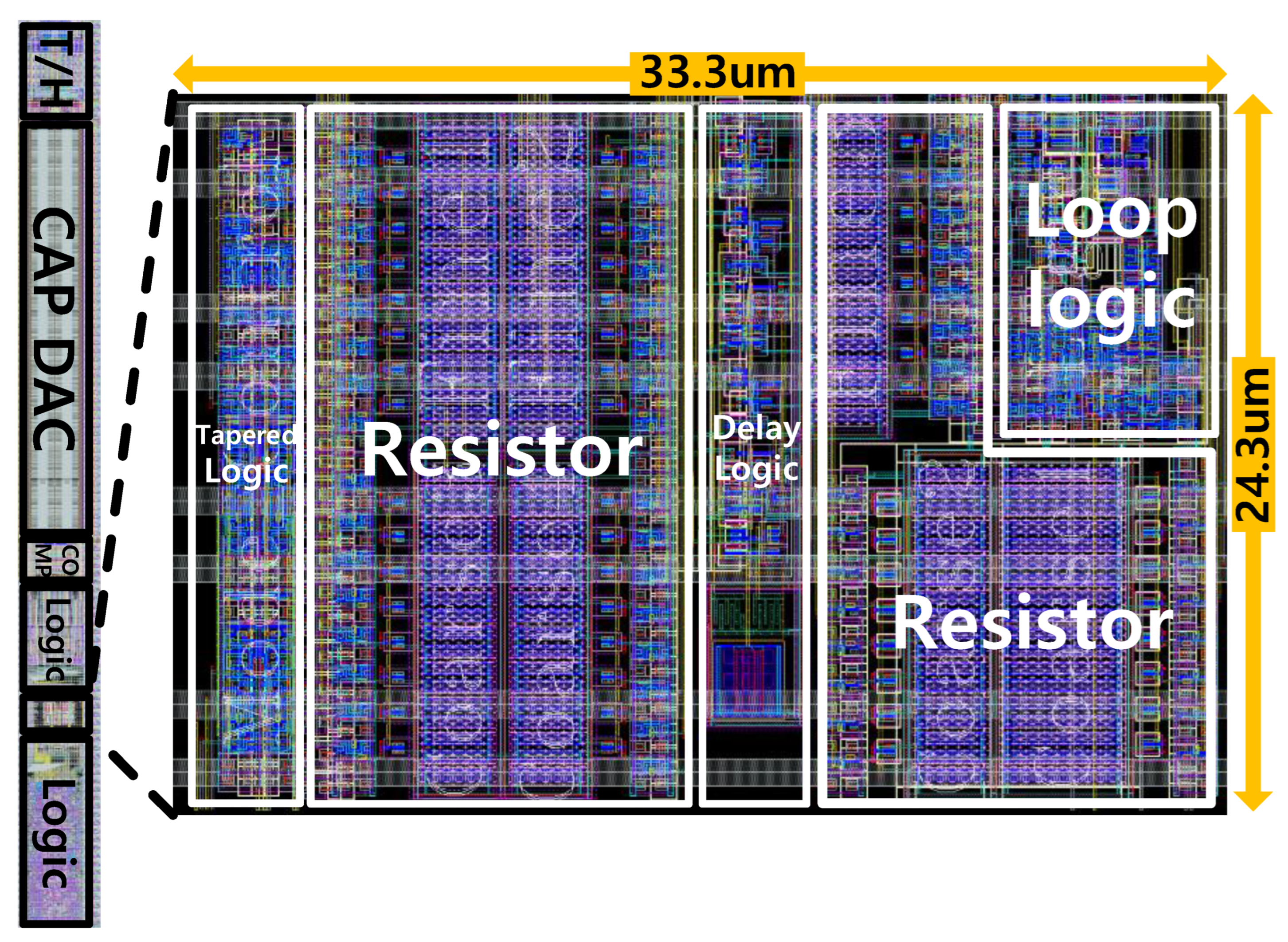
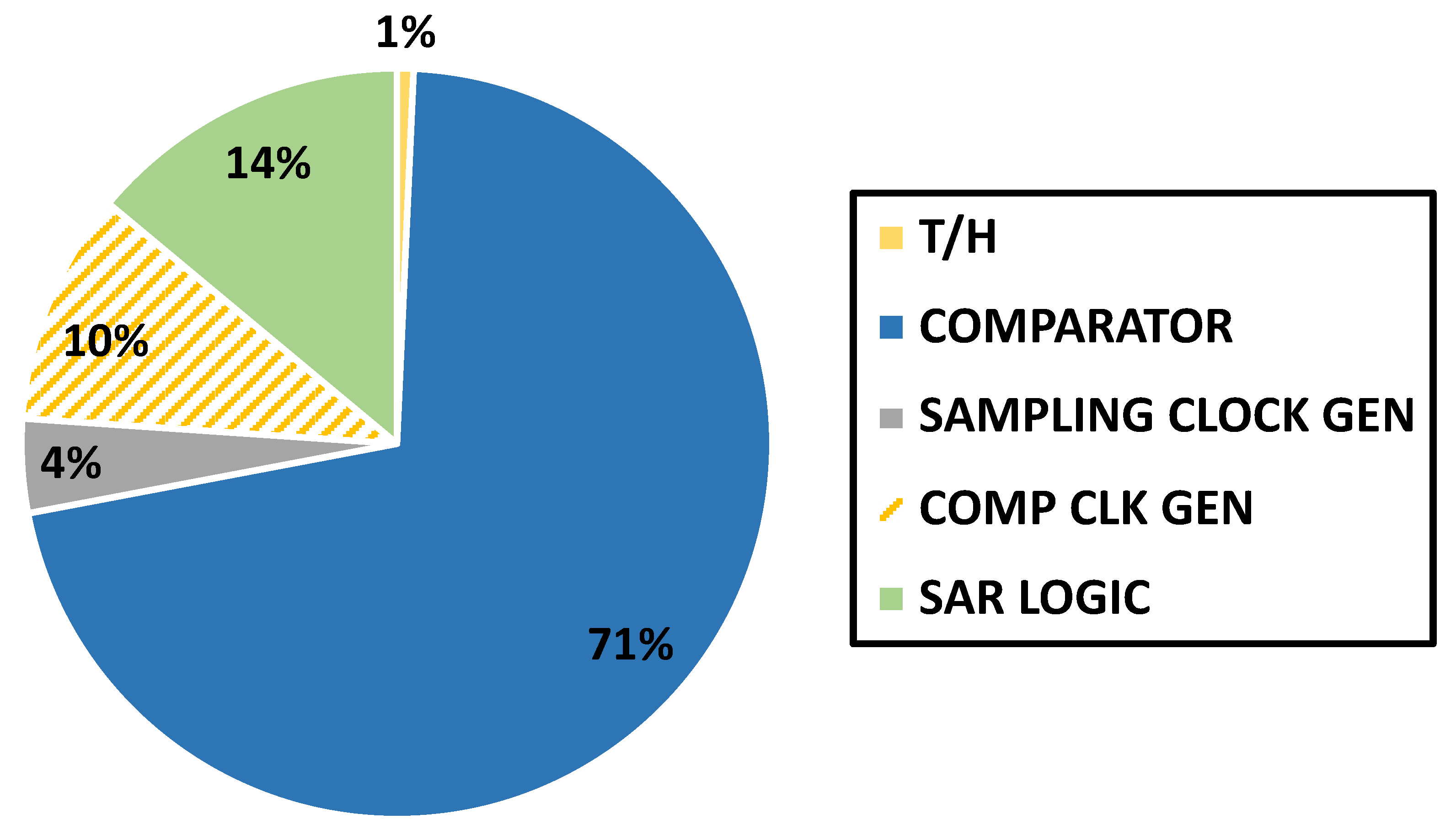
We designed the clock generator for the 12-bit 8 MS/s SAR ADC using the TSMC 55 nm CMOS process; its layout is presented in Figure 11. The clock generator occupies an area of 24.3 μ m × 33.3 μ m within the ADC slice of 1143 μ m × 81 μ m, designed in a rectangular shape to maximize the area efficiency of a multi-channel touch-IC ADC [22,23]. The T/H circuit was implemented using the bootstrap structure for high linearity performance [20], and a dynamic two-stage comparator was utilized for low noise [24]. The input referred noise is 113.8 μ   V r m s , and the comparator offset was simulated through Monte Carlo simulation. The histogram of Monte Carlo simulations with 400 samples showed a mean of −9.4 μ V, and a standard deviation of 1.7 mV. Additionally, the CDAC is designed with customized metal–oxide–metal (MOM) capacitors to achieve a unit capacitance of 1 fF. Figure 12 shows the power consumption of the ADC, and the total power consumption is 128.91 μ W at a supply voltage of 1 V. This is the post-simulation result of the proposed ADC, which includes the proposed COMP CLK GEN.
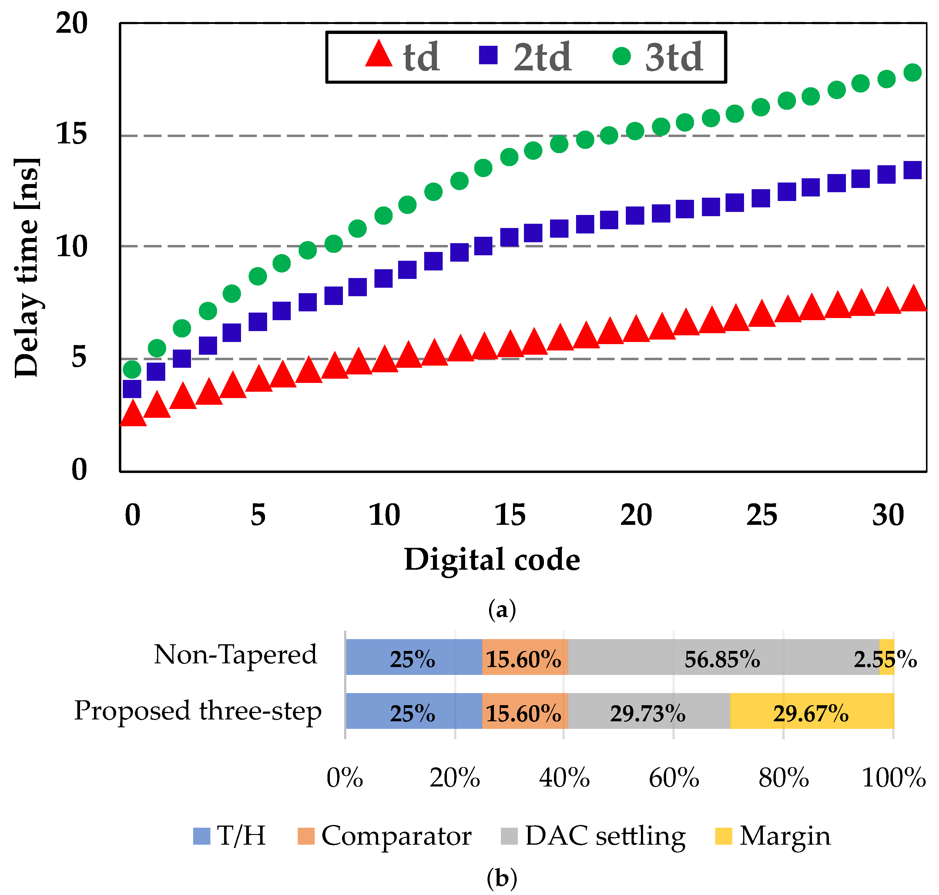
Figure 13a shows the simulated coarse step delay of our clock generation circuit shown in Figure 8. The minimum delay is 2.256 ns, and the maximum is 18.27 ns in 1 V supply. The fine delay comprises eight codes per coarse code and has about 50 ps steps that cover more than one coarse delay step. The simulated results for three delays ( t d , 2 t d , 3 t d ) are t d , 1.92   t d and 2.61   t d respectively, which are not exact integer multiples because of the incomplete voltage settling across pull-up and pull-down resistors and the fixed logic delay other than delay cell in Figure 6a. The energies required to generate the t d , 2 t d , 3 t d are found to be 111.5 fJ, 139.9 fJ, and 163.4 fJ, respectively, which means a small power overhead due to resistor sharing, compared to conventional three-stage delay generation, for which the power would linearly increase according to the number of delay stages. Based on the post-layout extracted delay time, the required DAC settling time is recalculated according to the procedure described in Section 2.2 and it is found that the required minimum DAC settling time of a three-step tapered bit period is reduced by 27.12% compared to that of the non-tapered one, as shown in Figure 13b. As a result, the increased margin increases the output impedance of R r e f or increases the sampling frequency.
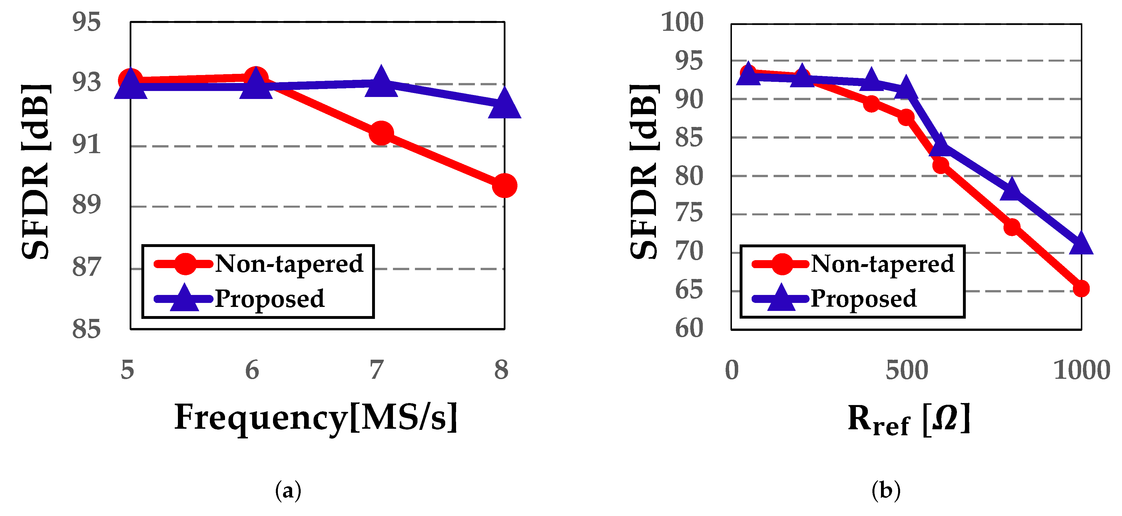
In Figure 14, the performance of our three-step tapering clocking scheme is verified by measuring the spurious free dynamic range (SFDR) over sampling frequency and R r e f . Figure 14a displays the SFDR with R r e f of 400 Ω at an input frequency of 331 kHz. Non-tapered and three-step tapering schemes yield an SFDR of over 92 dBc in the 6 MS/s ADC. However, for the 8 MS/s ADC, the SFDR performance of the conventional structure decreases by 3.4 dB, while the SFDR of the proposed structure only drops by 0.58 dB. Consequently, using the proposed three-step tapered bit period clock generation provides more margin in the conversion time, which allows higher sampling frequency.
Figure 14b shows the SFDR performance for different output impedance of R r e f . When R r e f is smaller than 200 Ω , both the conventional and proposed clock generation methods achieve 92 dB in SFDR. However, the performance degrades as R r e f increases. For the conventional clock generation method to achieve over 92 dB in SFDR, R r e f should be less than 200 Ω . On the other hand, the proposed clock generation method achieves 92 dB in SFDR even when R r e f is 400 Ω . As mentioned earlier, the size of R r e f in our design is set to 400 Ω , ensuring that the SFDR degradation is negligible as shown Figure 14b. The proposed method reduces the burden on the reference buffer and allows for a reduction in the reference buffer’s power that typically linearly scales with the required output conductance of the reference power. Additionally, CDAC mismatch influences SFDR performance, so it is crucial to minimize the impact of other factors, such as settling time, in order to achieve the desired ADC performance. The proposed technique, demonstrating reduced sensitivity to R r e f size, effectively allocates conversion time, consequently reducing performance degradation caused by the settling time.
Figure 15 displays the FFT spectra with transient noise for both the non-tapered and proposed clock generation schemes when the sampling frequency is 8 MHz and R r e f is 400 Ω . The input frequency is 331 kHz, and the peak-to-peak is 1.2 V. Both results yield 7983 points, and the range of the transient noise is from 2 kHz to 1 GHz. As a result, the proposed method achieves a 3.6 dB higher SFDR compared to the non-tapered methods under the same conditions.
A performance comparison table is shown in Table 2. Compared to the tapered technique [17,18], the proposed result has better time reduction. Furthermore, the proposed method is the only method that considers R r e f .

5. Conclusions

This paper proposes a technique for improving the performance of a 12-bit 8 MS/s asynchronous SAR ADC using a three-step tapered bit period. The required settling time of the CDAC in all conversion steps is analyzed and found to be exponentially reduced from MSB to LSB conversion, the impedance of the reference buffer, which leads us to propose a power-efficient three-step tapering clock generation circuit. The proposed technique reduces the minimum required total conversion time by an average of 48.08% compared to the non-tapered method, even using integer weights, in the three-step tapering technique. A resistance-sharing structure is presented to minimize the area increase caused by using three delays, resulting in only a 20.4% increase in the area. The proposed technique allows for an increase in the sampling frequency or power reduction in the reference buffer, with a more relaxed output impedance requirement.

Author Contributions

Conceptualization, H.K., S.L. and M.L.; methodology, H.K.; validation, H.K. and S.L.; formal analysis, H.K.; investigation, H.K.; writing—original draft preparation, H.K.; writing—review and editing, H.K.; visualization, H.K.; supervision, M.L.; project administration, M.L.; funding acquisition, M.L. All authors have read and agreed to the published version of the manuscript.

Funding

The EDA tool was supported by the IC Design Education Center (IDEC), Korea.

Data Availability Statement

All the data are reported/cited in the paper.

Acknowledgments

This work was supported by the the Commercializations Promotion Agency for R&D Outcomes (COMPA) grant funded by the Korea Government (MSIT) (No. 2021I500). (Corresponding author: Minjae Lee).

Conflicts of Interest

The authors declare no conflict of interest.

References

  1. Pietri, S.; Olmos, A.; Berens, M.; Boas, A.V.; Goes, M. A fully integrated touch screen controller based on 12b 825kS/s SAR ADC. In Proceedings of the Argentine School of Micro-Nanoelectronics, Technology and Applications, Bariloche, Argentina, 1–2 October 2009; pp. 66–70. [Google Scholar]
  2. Fan, H.; Heidari, H.; Maloberti, F.; Li, D.; Hu, D.; Cen, Y. High resolution and linearity enhanced SAR ADC for wearable sensing systems. In Proceedings of the IEEE International Symposium on Circuits and Systems (ISCAS), Baltimore, MD, USA, 28–31 May 2017; pp. 1–4. [Google Scholar]
  3. Liew, W.S.; Yao, L.; Lian, Y. A moving binary search SAR-ADC for low power biomedical data acquisition system. In Proceedings of the IEEE Asia Pacific Conference on Circuits and Systems (APCCAS), Macao, China, 30 November–3 December 2008; pp. 646–649. [Google Scholar]
  4. Pang, W.Y.; Wang, C.S.; Chang, Y.K.; Chou, N.K.; Wang, C.K. A 10-bit 500-KS/s low power SAR ADC with splitting comparator for bio-medical applications. In Proceedings of the IEEE Asian Solid-State Circuits Conference (A-SSCC), Taipei, Taiwan, 16–18 November 2009; pp. 149–152. [Google Scholar]
  5. Chang, Y.K.; Wang, C.S.; Wang, C.K. A 8-bit 500-KS/s low power SAR ADC for bio-medical applications. In Proceedings of the IEEE Asian Solid-State Circuits Conference (A-SSCC), Jeju, Republic of Korea, 12–14 November 2007; pp. 228–231. [Google Scholar]
  6. Chen, S.-L.; Villaverde, J.F.; Lee, H.-Y.; Chung, D.W.-Y.; Lin, T.-L.; Tseng, C.-H.; Lo, K.-A. A Power-Efficient Mixed-Signal Smart ADC Design With Adaptive Resolution and Variable Sampling Rate for Low-Power Applications. IEEE Sens. J. 2017, 17, 3461–3469. [Google Scholar] [CrossRef]
  7. Akbari, M.; Hashemipour, O.; Nazari, M.; Moradi, F.A. charge sharing–based switching scheme for SAR ADCs. Int. J. Circuit Theory Appl. 2019, 47, 1188–1198. [Google Scholar] [CrossRef]
  8. Yousefi, T.; Dabbaghian, A.; Yavari, M. An energy-efficient DAC switching method for SAR ADCs. IEEE Trans. Circuits Syst. II Express Briefs 2017, 65, 41–45. [Google Scholar] [CrossRef]
  9. Unno, Y.; Matsuura, T.; Kishida, R.; Hyogo, A. Examination of Incremental ADC with SAR ADC to Reduce Conversion Time with High Accuracy. In Proceedings of the International Symposium on Intelligent Signal Processing and Communication Systems (ISPACS), Taipei, Taiwan, 3–6 December 2019; pp. 1–2. [Google Scholar]
  10. Chen, S.-W.M.; Brodersen, R.W. A 6-bit 600-MS/s 5.3-mW Asynchronous ADC in 0.13-μm CMOS. IEEE J. Solid-State Circuits 2006, 41, 2669–2680. [Google Scholar] [CrossRef]
  11. Hu, Y.S.; Shih, C.H.; Tai, H.Y.; Chen, H.W.; Chen, H.S. A 0.6 V 6.4 fJ/conversion-step 10-bit 150MS/s subranging SAR ADC in 40nm CMOS. In Proceedings of the IEEE Asian Solid-State Circuits Conference (A-SSCC), Kaohsiung, Taiwan, 10–12 November 2014; pp. 81–84. [Google Scholar]
  12. Zhu, Y.; Chan, C.H.; Chio, U.F.; Sin, S.W.; Seng-Pan, U.; Martins, R.P.; Maloberti, F. A 10-bit 100-MS/s reference-free SAR ADC in 90 nm CMOS. IEEE J. Solid-State Circuits 2010, 17, 1111–1121. [Google Scholar] [CrossRef]
  13. Sekimoto, R.; Shikata, A.; Kuroda, T.; Ishikuro, H. A 40nm 50S/s–8MS/s ultra low voltage SAR ADC with timing optimized asynchronous clock generator. In Proceedings of the ESSCIRC (ESSCIRC), Helsinki, Finland, 12–16 September 2011; pp. 471–474. [Google Scholar]
  14. Huang, G.Y.; Chang, S.J.; Lin, Y.Z.; Liu, C.C.; Huang, C.P. A 10b 200MS/s 0.82 mW SAR ADC in 40nm CMOS. In Proceedings of the IEEE Asian Solid-State Circuits Conference (A-SSCC), Singapore, 11–13 November 2013; pp. 289–292. [Google Scholar]
  15. Wan, S.H.; Kuo, C.H.; Chang, S.J.; Huang, G.Y.; Huang, C.P.; Ren, G.J.; Ho, C.H. A 10-bit 50-MS/s SAR ADC with techniques for relaxing the requirement on driving capability of reference voltage buffers. In Proceedings of the IEEE Asian Solid-State Circuits Conference (A-SSCC), Singapore, 11–13 November 2013; pp. 293–296. [Google Scholar]
  16. Ju, H.; Lee, M. A 13-bit 3-MS/s asynchronous SAR ADC with a passive resistor based loop delay circuit. Electronics 2019, 8, 262. [Google Scholar] [CrossRef]
  17. Gu, W.; Zhou, H.; Lin, T.; Wang, Z.; Ye, F.; Ren, J. Power efficient SAR ADC with optimized settling technique. In Proceedings of the IEEE 56th International Midwest Symposium on Circuits and Systems (MWSCAS), Columbus, OH, USA, 4–7 August 2013; pp. 1156–1159. [Google Scholar]
  18. Janke, D.; Monk, A.; Swindlehurst, E.; Layton, K.; Chiang, S.H.W. A 9-Bit 10-MHz 28-μ W SAR ADC Using Tapered Bit Periods and a Partially Interdigitated DAC. IEEE Trans. Circuits Syst. II Express Briefs 2018, 66, 187–191. [Google Scholar] [CrossRef]
  19. Li, C.; Chan, C.H.; Zhu, Y.; Martins, R.P. Analysis of reference error in high-speed SAR ADCs with capacitive DAC. IEEE Trans. Circuits Syst. I Regular Pap. 2018, 66, 82–93. [Google Scholar] [CrossRef]
  20. Liu, C.C.; Chang, S.J.; Huang, G.Y.; Lin, Y.Z. A 10-bit 50-MS/s SAR ADC with a monotonic capacitor switching procedure. IEEE J. Solid-State Circuits 2010, 45, 731–740. [Google Scholar] [CrossRef]
  21. Shehzad, K.; Verma, D.; Khan, D.; Ain, Q.U.; Basim, M.; Kim, S.J.; Lee, K.Y. Design of a low power 10-b 8-MS/s asynchronous SAR ADC with on-chip reference voltage generator. Electronics 2020, 9, 872. [Google Scholar] [CrossRef]
  22. Park, J.; Hwang, Y.H.; Oh, J.; Song, Y.; Park, J.E.; Jeong, D.K. A mutual capacitance touch readout IC with 64% reduced-power adiabatic driving over heavily coupled touch screen. IEEE J. Solid-State Circuits 2019, 54, 1694–1704. [Google Scholar] [CrossRef]
  23. An, J.S.; Ra, J.H.; Kang, E.; Pertijs, M.A.; Han, S.H. A capacitive touch chipset with 33.9 dB charge-overflow reduction using amplitude-modulated multi-frequency excitation and wireless power and data transfer to an active stylus. In Proceedings of the IEEE International Solid-State Circuits Conference(ISSCC), San Francisco, CA, USA, 16–20 February 2020; pp. 430–432. [Google Scholar]
  24. Liu, C.C.; Kuo, C.H.; Lin, Y.Z. A 10 bit 320 MS/s low-cost SAR ADC for IEEE 802.11 ac applications in 20 nm CMOS. IEEE J. Solid-State Circuits 2017, 50, 2645–2654. [Google Scholar] [CrossRef]
Figure 1. Structure of asynchronous SAR ADC.
Electronics 12 01863 g001
Figure 2. (a) Capacitive DAC array with reference buffer and (b) modeling circuit in ith conversion cycle.
Electronics 12 01863 g002
Figure 3. A comparison between considering reference buffer or not.
Electronics 12 01863 g003
Figure 4. Required setting time according to R, R r e f with MSB conversion cycle.
Electronics 12 01863 g004
Figure 5. Delay time with three-step and i n t e g e r   three-step technique when R r e f = 400 Ω .
Electronics 12 01863 g005
Figure 6. (a) Comparator clock generation circuit [16,21]. (b) SAR control logic [20]. (c) Timing diagram of comparator clock generation and control logic.
Electronics 12 01863 g006
Figure 7. (a) Conceptual block diagram of a delay cell. (b) Three-step tapered control generator.
Electronics 12 01863 g007
Figure 8. Schematic of the proposed three-step bit period delay cell.
Electronics 12 01863 g008
Figure 9. The schematic of the blocking method in proposed delay cell.
Electronics 12 01863 g009
Figure 10. Calculation and simulation result of required settling time according to R r e f and location of capacitive DAC.
Electronics 12 01863 g010
Figure 11. Layout design of proposed three-step tapered bit period clock generation in SAR ADC.
Electronics 12 01863 g011
Figure 12. Power breakdown of ADC.
Electronics 12 01863 g012
Figure 13. (a) Post-simulation result with three-step tapered bit period clock generation according to digital code, (b) timing allocation when R r e f = 400 Ω in 6 MS/s SAR ADC.
Electronics 12 01863 g013
Figure 14. The 12-bit ADC SFDR performance according to (a) sampling frequency when R r e f = 400 Ω , (b) impedance of the R r e f at 8 MS/s.
Electronics 12 01863 g014
Figure 15. FFT plot with transient noise (a) using non-tapered method and (b) using proposed method when R r e f is 400 Ω at 12-bit 8 MS/s SAR ADC.
Electronics 12 01863 g015
Table 1. Minimum required total conversion time according to different tapering techniques.
Rref200 Ω300 Ω400 Ω500 Ω600 ΩAverage
Technique
Non-tapered
(one-step)
47.87 ns
(100%)
71.32 ns
(100%)
94.76 ns
(100%)
118.21 ns
(100%)
141.66 ns
(100%)
94.76 ns
(100%)
All-tapered11.23 ns
(23.45%)
16.58 ns
(23.25%)
21.98 ns
(23.19%)
27.36 ns
(23.15%)
38.16 ns
(23.11%)
21.98 ns
(23.23%)
Limited all-tapered27.49 ns
(57.42%)
30.8 ns
(43.19%)
34.61 ns
(36.53%)
38.61 ns
(32.66%)
47.89 ns
(30.32%)
35.88 ns
(40.02%)
Two-step29.38 ns
(61.36%)
33.81 ns
(47.41%)
43.79 ns
(46.21%)
50.8 ns
(42.98%)
69.91 ns
(42.69%)
43.65 ns
(48.13%)
Three-step27.66 ns
(57.78%)
31.00 ns
(43.47%)
36.75 ns
(38.78%)
41.12 ns
(34.78%)
56.15 ns
(34.8%)
37.17 ns
(41.92%)
Four-step47.87 ns
(100%)
71.32 ns
(100%)
36.07 ns
(38.06%)
42.28 ns
(35.76%)
55.92 ns
(34.79%)
50.69 ns
(61.72%)
Integer three-step32.2 ns
(67.26%)
32.2 ns
(45.15%)
40.6 ns
(42.84%)
50.4 ns
(42.64%)
60.2 ns
(42.5%)
43.12 ns
(48.08%)
Table 2. Performance comparison table.
ProposedNon-Tapered[13] *[16] *[17][18] *
Technology55 nm55 nm40 nm40 nm65 nm180 nm
Supply (V)110.7 **1.11.21
Frequency (MHz)88235010
Resolution (bit)1212913129
Number of delay code2562563225611
Number of step318128
Time reduction (%)47.70Not-mention02532.6
Delay cell structurePoly-resistorPoly-resistorInverter chain, CapacitorPoly-resistorInverter chainCurrent starved
R r e f ( Ω )400400NeglectedNeglectedNeglectedNeglected
SFDR (dB)89.886.2-6882.171.6
SNDR (dB)71.269.951.6159.470.655.5
Power ( μ W)128.91-5.5671663-
Area (mm 2 )0.093-0.1920.054-0.074
* Measured result. ** Analog supply is 0.6 V, digital supply is 0.7 V.
Disclaimer/Publisher’s Note: The statements, opinions and data contained in all publications are solely those of the individual author(s) and contributor(s) and not of MDPI and/or the editor(s). MDPI and/or the editor(s) disclaim responsibility for any injury to people or property resulting from any ideas, methods, instructions or products referred to in the content.