Abstract
This paper compares the cost and efficiency of two inverter topologies for a 5-kW grid-connected solar inverter application: the Conventional H-Bridge Inverter (CHB) and the Cascaded H-Bridge Multilevel Inverter (CHBMLI). Emphasis is put on power switches and passive elements with a detailed study of the losses. Both designs respect the same constraints (cost, efficiency, and junction temperature of the transistors) to ensure a fair comparison between both topologies. The work highlights the important parameters when choosing the components (MOSFETs, capacitors, and magnetic cores for the inductors). The DC-link voltage ripple and the output AC current ripple are the key parameters for the design of the passive elements (capacitors and inductors). On top of that, the transistors MOSFETs are chosen, in both topologies, to limit the conduction losses (by selecting the ) and the switching losses (by selecting the and ). Real components are picked in order to make the comparison as complete as possible. Numerical simulations are performed using the MATLAB platform. All equations and parameters are provided. A CHBMLI prototype was built with eight independent H-Bridges to validate the proposed design with thermal and efficiency measurements.
1. Introduction
The energy crisis issue due to the need to reduce CO2 emissions and the shortage of fossil fuels has led most countries around the world to consider the use of renewable energy (solar PV (photovoltaics), wind power, hydropower, biopower) for electricity production. In 2019, over 200 GW of renewable energy was installed worldwide, including 120 GW of solar PV [1].
The PV inverter represents 10 to 15% of the total cost of a grid-connected PV system [2]. It is used to convert DC power from solar panels into AC power to be fed into the grid. Many solar inverter configurations can be defined [3,4,5]. Among them, the Central/Conventional H-Bridge Inverter (CHB) [6] and the Cascaded H-Bridge Multilevel Inverter (CHBMLI) [7] are studied in this paper. A Central H-Bridge Inverter usually consists of two power stages: a DC−DC boost converter as the front stage to get sufficient DC-bus voltage [8] and obtain a wider input voltage tracking range; and an inverter as the second stage to generate the AC utility line voltage. As an alternative to the boost DC−DC converter, a step-up transformer can be used to reach the grid voltage. This topology can reach peak efficiencies of up to 96% [9,10].
A cascaded inverter consists of several converters connected in a series, and it has many advantages in medium and large grid-connected PV systems [7,11,12,13,14]. In the CHBMLI topology, those converters are H-bridges. A DC−DC converter can be added between the solar panel and the H-bridge [15]. This helps to stabilize the voltage at the H-bridge from temperature and irradiation variations and to perform local Maximum Power Point Tracking (MPPT) [16,17,18]. On top of that, due to its stair-shaped output waveform, the CHBMLI provides low switching voltages, which greatly reduces the output filter [19,20].
Furthermore, control techniques, such as Selective Harmonics Elimination Pulse Width Modulation (SHE-PWM), can be used to remove current harmonics and reduce the Total Harmonic Distortion (THD) [21]. As the Conventional H-Bridge Inverter switches higher voltages (), the output filter is costly and bulky [6]. However, the CHBMLI requires more transistors and drivers than the conventional H-bridge.
In the literature, CHBMLI prototypes have been developed and studied [13,22]. However, the number of modules is often limited (up to 5), and the switching frequency is also limited (up to 4 kHz). Those prototypes are, thus, not suited for a grid-tied solar application on the 230 V AC main grid. Most solar inverters on the market are based on the conventional H-Bridge topology. In a previous paper, the authors have demonstrated that, with a specific hardware architecture, it is feasible to control a CHBMLI with at least 8 modules (and up to 20) with a switching frequency of 20 kHz [23]. The prototype was built using low-cost local electronics on each H-Bridge without the need for isolated measurements and isolated drivers compared to other prototypes presented in the literature [24,25]. The prototype developed by the authors makes the CHBMLI suitable for a grid-tied solar application on the 230 V AC main grid.
Even though both topologies are quite familiar in the literature, there are no studies comparing, in detail, the design of both converters in terms of size and complete cost of passive elements and MOSFETs, with a 20 kHz switch and a high number of modules.
The aim of this paper is to present a comparison of the standard H-Bridge Inverter and the CHBMLI for solar applications under the same sizing constraints. For the study, we consider an output power of 5 kW without DC−DC converters for both topologies. For both topologies, a series of constraints (Table 1) is applied to the waveforms and the overall efficiency. First, the passive elements (DC-link capacitor and output inductor ) are designed based on the DC-link voltage ripple and the output AC current ripple . The value of is set to 4% of the optimum DC-link PV voltage in both topologies. The impact of this voltage ripple on solar power extraction is detailed in Section 2. The value of is set to 10% of the peak output grid current . Furthermore, the MOSFETs and the drivers are both chosen to limit the conduction losses (by selecting the ) and the switching losses (by selecting the and ). Each loss is limited to 1% of the nominal output power . In both cases, the junction temperature of MOSFETs is studied, and a heatsink is selected to limit this value to 100 °C. The values of , , and are presented in the next paragraph. Finally, based on those constraints, a series of comparisons are made in terms of cost, volume, and overall efficiency. Experimental measurements of the temperature rise, efficiency, and waveforms of the CHBMLI prototype are performed.

Table 1.
Design constraints for both topologies.
Solar module, grid, and inverter parameters used in this paper are presented in Table 2. The two topologies presented in this study use LR460HPH365M solar panels placed in a series. When operating without a boost converter, the voltage of all the panels placed in a series must be higher than the maximum grid voltage. A 10% tolerance is considered. Furthermore, for a given temperature, the optimum voltage decreases when solar irradiation decreases. However, for low irradiation (under 100 W/m2), the output power is less sensitive to voltage variation around the optimum point. Thus, the voltage to maximize the power extraction when the irradiation is 10% of the nominal one is chosen as the minimum voltage panel for the design. On top of that, an extra panel is added to improve the overall robustness. According to that, the following equation gives the number of solar panels required for a grid-tied inverter:
where is the number of solar panels, is the RMS grid voltage (V), is the grid voltage tolerance (%) and is the minimum voltage required to ensure MPPT at 100 W/m2 and 25 °C (V).
Table 2.
Solar module, grid, and inverter parameters.
Section 2 describes the design of the conventional H-Bridge based on parameters presented in Table 2. Section 3 applies the same design scheme as the CHBMLI. Section 4 gives a comparison between the two topologies. Section 5 presents the CHBMLI prototype and experimental measurements. Section 6 concludes the work.
2. Design of the Conventional H-Bridge
2.1. Main Characteristics
The H-Bridge is a well-known topology that converts DC into AC voltage [6,20]. The complete converter can be done with an H-Bridge driver and four N-channel MOSFETs. An inductor is used to filter the output grid current, and capacitors placed on the DC link limit the voltage ripple. For a 5-kW application, these passive elements represent an important part of the overall cost and volume of the converter. As for the semiconductors, power losses and temperature rise must be taken into account.
The conventional H-Bridge grid-tied solar inverter is shown in Figure 1. The DC side of the H-Bridge converter is powered by an array of photovoltaic (PV) panels in series. The PV voltage is stabilized by the capacitor connected in parallel. The AC side of the H-Bridge converter is connected to the single-phase grid through an L filter. The output current of the PV array and the output voltage of the H-Bridge converter can, respectively, be described by Equations (2) and (3):
where and are, respectively, the output current and the output voltage of the PV array. and are, respectively, the input current and output voltage of the H-Bridge converter. is the current through the capacitor , is the voltage across the inductor . and are, respectively, the grid current and the grid voltage.

Figure 1.
Configuration of the conventional H-Bridge grid-tied solar inverter.
In this paper, solar production is considered with a unity power factor. Thus, the grid current and grid voltage are in phase and are defined by Equations (4) and (5):
where and are, respectively, the grid RMS current and the grid RMS voltage. is the grid angular frequency.
2.2. Passive Elements
2.2.1. DC-Link Capacitor
The DC-link capacitor is the first passive element that needs to be properly sized. It is a compromise between volume/cost and voltage ripple on the DC side of the H-Bridge converter. The equation for sizing the capacitor is presented in [26]:
where is the optimum current (A), is the 100 Hz voltage ripple (V) and is the grid angular frequency ().
When selecting the voltage ripple value , it is important to consider its impact on PV power extraction. Figure 2 presents the evolution of the mean output power with the voltage ripple [23]. This figure was obtained considering the average output power of a single solar panel for a given voltage ripple around the optimum voltage and for a given solar irradiance. For the study conducted in this paper, we chose to limit the power drop to 1% of the Maximum Power Point. To achieve this, Figure 2 shows that the voltage ripple should not exceed 4%. To limit the voltage ripple to 4%, the filter capacitor must be at least:
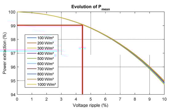
Figure 2.
Power drop and voltage ripple [23].
For the capacitor voltage rating, a 30% tolerance is applied from the DC link optimal voltage. Thus, 600 V capacitors are used. Capacitors chosen for both topologies in this paper are TDK aluminum electrolytic capacitors. For 600 V capacitors, B43541 capacitors are considered. As /600 V capacitors do not exist, several smaller capacitors are placed in parallel. Considering the characteristics of those capacitors, particularly their Equivalent Series Resistance (ESR), the design of the inverter must take into account the associated losses. It is important to notice that, in a power converter, the cost of the capacitors is proportional to the energy stored. Thus, for a given total capacitor and voltage values, choosing many small capacitors has a similar cost as choosing a few big capacitors. Typical parameters of the capacitors are presented in Table 3.
Table 3.
Capacitor parameters (TDK aluminum electrolytic, B43541).
The losses in the function of the capacitor value (equations are detailed further in the article) are shown in Figure 3. First, the figure shows that the total ESR (at ) of all capacitors placed in parallel for a given energy to store is independent of the number of parallel capacitors at the same global equivalent capacitor value: a high number of low-value capacitors or a low number of high-value capacitors. Indeed, for the same voltage rate, the ESR decreases as the capacitor value increases at the same rate. The second plot of Figure 3 highlights that whatever the configuration, total capacitor losses remain the same. However, losses per capacitor increase when the number of capacitors decreases. The temperature rise of each capacitor, which will greatly affect the lifespan of the inverter, increase when the number of capacitors decreases. Thus, / capacitors are the optimal choice, and 21 capacitors are placed in parallel. For both designs, the tolerance (20%) of the capacitor’s value is not taken into account.

Figure 3.
ESR and losses according to the capacitor value.
The capacitor losses are mostly due to the ESR.
where is the number of capacitors placed in parallel (), is the ESR at of a single capacitor () and is the RMS current through the capacitor at . Numerical simulations with MATLAB provide that: .
The capacitor losses lead to a temperature rise for each capacitor [27]:
where is the surface heat rise (°C), is the heat radiation factor ( and , is the surface area of the capacitor ( and is the factor of the temperature difference between the core and surface ().
2.2.2. Output Inductor
The grid-tied solar inverter requires an output low-pass filter to eliminate the current ripple around the switching frequency. The values of the current ripple fundamental and its harmonics have to comply with the IEEE 1547 standards. The three main low-pass filters presented in the literature are the L-filter, the LC-filter, and the LCL-filter [28]. The LCL-filter is considered the most interesting due to its independence from the grid impedance and a better output response with the same inductance. However, designing such a filter has to consider many constraints, such as the resonance phenomenon or the capacitor’s reactive power. As the aim of this paper is to compare two topologies, the same type of output filter is used. To ease the comparison, a classic L-filter will be designed for both topologies. It is important to note that elements of comparison (losses or size) are still relevant if an LC-filter or an LCL-filter is used for design.
The system has a unity power factor, and the control scheme adopted is a unipolar PWM. The inductance of the L-filter is given by the following formula [29]:
where is the maximum current ripple (A) and is the switching frequency (Hz). The maximum current ripple is chosen as 10% of the peak-rated inverter current (. A complete Fast Fourier Transform (FFT) analysis would normally be required to ensure that the grid-tied inverter complies with the IEEE 1547 standards for current harmonics. However, for comparison purposes, limiting the current ripple at the switching frequency is sufficient. Moreover, the switching frequency of a grid-tied solar inverter with an output power of a few kW is often chosen within the range of 10 to 50 kHz. This choice is a compromise between the size of the output filter, the switching losses, the MCU performances, the leakage current etc. In this paper, the switching frequency () is set to 20 kHz for both topologies.
The design of the inductor is done by using magnetic cores from the Ferroxcube Data Handbook 2013 [30]. As there is no magnetic core big enough to design a 1.9 mH/30 A inductor, two /30 A are placed in series. The magnetic core of a single inductor is made using two E cores with an air gap on both center legs, as presented in Figure 4. For a 20 kHz application, the 3C90 ferrite has the maximum saturation magnetic field ( at ).
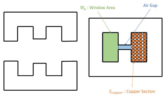
Figure 4.
Magnetic core of the inductor.
In a /30 A inductor, the energy stored (W) in the air gap is:
The required air gap volume is:
where is the vacuum permeability (H/m), is the saturation magnetic field of the chosen core (3C90).
The chosen magnetic core is E71/33/32 with a air gap. The effective area of the core is . The datasheet of the core provides that the inductance factor is:
The number of turns to reach a inductance is:
Given that the wiring must fit within the window area of the magnetic core, the copper section () is given by:
where is the window area (=) and K is the fill factor (=). This copper section had no issue handling the current.
The design of the coil must take into account the type of conductor chosen (litz wire or not). Indeed, for a cylindrical conductor with an alternating current, the current density decreases exponentially from the surface toward the inside. This phenomenon, known as the skin effect, depends on the type of conductor and the frequency of the current [31]. It is characterized by the skin depth at temperature , which must be higher than the radius of the conductor in order to minimize resistive losses.
where is the resistivity () of the conductor at temperature , is the relative magnetic permeability of the conductor (1 for copper), is the permeability of free space () and is the frequency of the current ().
The copper resistivity depends on its temperature:
where is the operating temperature (K), is the reference temperature (K), is the temperature coefficient (), is the resistivity of the conductor at () and is the resistivity of the conductor at ().
For copper, and .
Thus:
The conductor used here has a much thinner radius (1.5 mm). There is no need to use litz wire for this application. Furthermore, the proximity effect is neglected in this topology due to the low frequency (50 Hz) of the AC current and the low RMS value of the high frequency (20 kHz) ripple (limited to 10% of the nominal current) [31].
Now that both the magnetic cores and the copper section have been designed, the copper and core losses of the two inductors can be estimated:
where is the average length of a turn (=) and is the copper resistivity () at 75 °C.
The core losses can be calculated as follow:
where are the core losses () of the 20 kHz ripple curent , is the effective volume () of the magnetic core and is the core losses density () of the magnetic core for a given amplitude of the flux density B (T) and a given frequency f (Hz). The amplitude is calculated with the following formula [32]:
The datasheet provides:
With , and .
Thus, the core losses are:
The low core losses of the inductor are due to the low ripple current . A higher ripple would lead to a higher amplitude of the flux density . The total losses in the inductor are:
The characteristics of passive elements for the conventional H-Bridge are summarized in Table 4.
Table 4.
Conventional H-Bridge design.
2.3. MOSFET
The N-channel MOSFET chosen for this application must fulfill several requirements. First, a 25% tolerance is set for the maximum drain-to-source voltage based on the maximum DC-link voltage when all panels are at their open-circuit voltage. On top of that, a 25% tolerance is applied for the maximum drain current based on the maximum output current when all panels are at their optimum voltage under optimum weather conditions. Thus, the chosen MOSFET is at least a 650 V/35 A transistor.
In a grid-tied inverter with a conventional H-Bridge, the key power-loss contributors are the conduction losses, the switching losses, and the passive element (capacitors and inductors) losses. Indeed, the high maximum output current () contributes to the maximal conduction losses, and the high maximum DC-link voltage ( contributes to the maximal switching losses. Most grid-tied solar inverters available on the market can reach a peak efficiency of around 97.5% at the nominal power level. For the design, it is decided that conduction and switching losses should not exceed 1% each of the total output power, and passive elements losses should not exceed 0.5% of the total output power. The efficiency at the nominal power point is thus set to be around 97.5%.
2.3.1. Conduction Losses
The conduction losses can be calculated using a MOSFET approximation with drain-source on-state resistance of . With a unipolar PWM, half of the transistors are on at any time. For each closed transistor, the complementary transistor is open. The conduction losses can be defined with the following formula:
Then (with a 100 °C junction temperature) is limited by the following equation:
2.3.2. Switching Losses
The switching losses can be calculated as follow [33]:
where are the switching losses, and are, respectively, the turn-on and turn-off energy for the MOSFET, and are, respectively, the turn-on and turn-off energy for the body diode during switching phases and is the switching frequency.
The worst-case turn-on losses in a power MOSFET can be calculated as the sum of the switch-on energy without considering the reverse recovery process and the switch-on energy caused by the reverse recovery of the freewheeling diode [33]:
where is the rising current time (s) and is the falling voltage time (s) during switching phase, is the reverse recovery charge (C). The reverse recovery charge is selected for a 100 °C junction temperature and a rating current of . The datasheet of a transistor usually only provides the reverse recovery charge for a 25 °C junction temperature.
The switch-off losses in the diode are normally neglected ( due to the low diode forward voltage compared to the DC-link voltage. The turn-on energy of the diode consists mostly of the reverse recovery energy:
The switch-off energy losses in the MOSFET can be calculated in the same way.
where is the falling current time (s) and is the rising voltage time (s) during switching phase.
By substituting (29), (31), and (32) into (28), the total switching losses are:
The rise time and fall time of the voltage are the only parameters that can be handled by external circuitry. Indeed, an external gate resistor is added between the driver and the gate of the MOSFET. It limits the noise and ringing in the gate drive path. However, increasing the rising and falling times leads to higher switching losses. On top of that, if transition times can no longer be neglected against the switching period , control issues may appear. For design purposes in this paper, the dv/dt of the transistor is limited to :
For information, the external gate resistor can be calculated based on the following equations [34]:
With:
where is the external gate resistor (), is the internal gate resistor (), is the voltage of the driver circuit (12 V), is the Miller voltage (V), is the gate-drain capacitor (F) for a given voltage (V).
2.3.3. MOSFET Choice
The transistor chosen for the conventional H-Bridge design that complies with these constraints is the NTHL040N65S3F. Table 5 provides the parameters of the NTHL040N65S3F that are used to calculate all remaining losses.
Table 5.
Parameters of the NTHL040N65S3F.
The conduction and switching losses are:
The dead time losses depend on the body diode’s forward voltage during phases when both transistors of a leg are off:
where and are, respectively, the rising dead time (s) and falling dead time (s).
In unipolar PWM, gate charge losses for all the transistors are provided by the H-Bridge driver:
where is the gate charge (C).
The parasitic capacitance of the MOSFET is also responsible for extra losses:
Approximately 3 W (including the gate charge losses) are necessary for the control side of the converter (microcontroller, sensors, and relays):
3. Design of the Cascaded H-Bridge Multilevel Inverter
3.1. Main Characteristics
The CHBMLI topology consists of several H-Bridge converters in a series. Each DC link is fed by a single solar panel. A capacitor, placed in parallel with the panel, is required to store the energy during phases when the H-Bridge’s module output is bypassed [13]. The topology is presented in Figure 5.

Figure 5.
Cascaded H-Bridge Multilevel Inverter (CHBMLI) configuration.
3.2. Passive Elements
3.2.1. DC-Link Capacitor
The process of selecting the capacitor value is based on limiting the voltage ripple to 4% (the same limit as for the conventional H-Bridge). On the multilevel topology, the voltage ripple is calculated from the voltage of a single solar panel at MPP (Maximum Power Point): . The value of the capacitor per H-Bridge is calculated with the following formula:
For 50 V capacitors, B41505 capacitors are considered (aluminum electrolytic capacitors from TDK). The capacitor is made by paralleling four capacitors ().
The capacitor losses are mostly due to the ESR. The total capacitor losses are the sum of the capacitor losses per H-Bridge. On top of that, the ESR of those capacitors is estimated with an RMS capacitor current at the switching frequency of each H-Bridge.
where is the total ESR of the four () capacitors at () and is the RMS current through the capacitor. Numerical simulations with MATLAB provide that: .
The capacitor losses lead to a temperature rise for each capacitor:
where is the surface heat rise (°C), is the heat radiation factor ( and , is the surface area of the capacitor ( and is the factor of the temperature difference between the core and surface ().
3.2.2. Output Inductor
As for the conventional H-Bridge, the switching frequency of the converter is set to 20 kHz, and the current ripple is chosen as 10% of the rated inverter current. The inductor is calculated by using the following equation:
The design of the inductor is done by using magnetic cores from the Ferroxcube Data Handbook 2013. As for the two inductors of the conventional H-Bridge, the magnetic core is made using two E cores with an air gap between both center legs. As for the design of the inductor in the conventional H-Bridge, a 3C90 ferrite is used.
In a /30 A inductor, the energy stored (W) in the air gap is:
The required air gap volume is:
The chosen magnetic core is E42/33/20 with a air gap to reach the proper air-gap volume. The effective area of the core is . The datasheet of the core provides that the inductance factor is:
The number of turns for a inductance is:
Given that the wire must fit within the window area (=) of the magnetic core, the copper section () is given by:
Now that both the magnetic cores and the copper section have been designed, the copper and core losses can be estimated:
The core losses can be calculated as in Section 2. The low ripple current leads to a low amplitude of the flux density at 20 kHz (). This leads to a very low power loss density of the magnetic core. On top of that, the volume of the inductance is also very low. Thus, the core losses are neglected:
The total inductor losses are:
The characteristics of the chosen topology and its passive elements are summarized in Table 6.
Table 6.
Cascaded H-Bridge Multilevel Inverter design.
3.3. MOSFET
For the N-channel MOSFET design, and as for the conventional H-Bridge, a 25% tolerance is applied on the maximum drain to source voltage and the maximum drain current. Thus, the chosen MOSFET is at least a 50 V/35 A transistor.
As for the design of the conventional H-Bridge, it is set that conduction and switching losses should not exceed 1% of the total output power, and passive element losses should not exceed 0.5% of the total output power.
3.3.1. Conduction Losses
Given the fact that H-Bridge converters are used in the CHBMLI instead of only one for the conventional H-Bridge under standard conditions, the current is passing through half the transistors of each H-Bridge. The limit for conduction losses is based on the following equation:
Then (with a 50 °C junction temperature) is limited by:
3.3.2. Switching Losses
The full system switching losses are expressed by the following equation:
On average, each H-Bridge switches around times per second.
3.3.3. MOSFET Choice
The transistor chosen for the CHBMLI that complies with these constraints is the DMTH6004SK3. Table 7 provides the parameters of the DMTH6004SK3 that are used to calculate all the remaining losses.
Table 7.
Parameters of the DMTH6004SK3.
The conduction and switching losses are:
The dead time losses depend on the body diode’s forward voltage during phases when both transistors of a leg are off:
In unipolar PWM, gate charge losses for all the transistors are provided by the H-Bridge driver:
The parasitic capacitance of the MOSFET is also responsible for extra losses:
Approximately 300 mW (including the gate charge losses per H-Bridge) are necessary for the control side of each converter (microcontroller, sensors, communication), and 3 W are necessary for the Master control of the full converter (microcontroller, communication, and relays):
4. Discussion
The aim of this section is to compare the design of the two converters in terms of size and cost for the passive elements on the basis of simulations. Efficiencies of both converters are also assessed for the full range of output power. Finally, the costs of MOSFETs (+driver and heatsink) for both converters are compared. Simulations of both topologies are performed under the MATLAB/SIMULINK platform.
4.1. Circuit Simulations
The waveforms of both converters are shown in Figure 6. The parameters used for the two simulations are presented in Table 2. The multilevel ability of the CHBMLI offers much more possibilities in terms of reducing the harmonics than the Conventional H-Bridge [35]. However, the comparison made in this study only considers the grid current ripple and neglects the harmonics in order to use the control algorithm for the CHBMLI presented by the authors in a previous study [36], as these algorithms do not yet include specific harmonics elimination. Several control algorithms, such as Selective Harmonics Elimination Pulse Width Modulation (SHE-PWM), can be used to remove current harmonics and reduce Total Harmonic Distortion (THD) [21]. Conventional control with integrated control loops [37] is used for the Conventional H-Bridge (CHB) with a unipolar PWM.
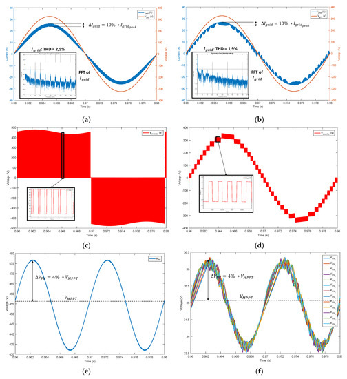
Figure 6.
(a) Grid Voltage (red) and Grid Current (blue) for the CHB (b) Grid Voltage (red) and Grid Current (blue) for the CHBMLI (c) Inverter Voltage (red) for the CHB (d) Inverter Voltage (red) for the CHBMLI (e) PV Voltage for the CHB (blue) (f) PV Voltages for the CHBMLI.
The Conventional H-Bridge (CHB) and the CHBMLI both have a maximum output current ripple limited to 10% of the peak output current (Figure 6a,b), which validate the design of both inductors. Furthermore, for both simulations, the current (blue) is set in phase with the grid voltage (red). The THD of the CHBMLI (1.9%) is slightly lower than the THD of the CHB (2.5%). This is due to the control algorithm that mitigates some harmonics. However, the THD of the CHBMLI could be further improved by using Selective Harmonics Elimination [21]. The output waveform of both inverters is presented in Figure 6c for the CHB and Figure 6d for the CHBMLI. The CHB has a three-level output voltage with high switching voltages (), and the CHBMLI has a stair-shaped output waveform with low switching voltages (). The waveform of the CHBMLI, almost sinusoidal, visually explains why the inductor is much lower for a similar grid current ripple than the CHB. Finally, both converters have an identical DC-link voltage ripple limited to 4% of the optimal voltage (Figure 6e,f), which validates the design of both capacitors. In the case of the CHBMLI, the converter regulates each DC-link voltage of the modules around with the same ripple . The waveforms of the DC-link voltages of the CHBMLI are not as sinusoidal as the one of the CHB, because the average switching frequency of each module is .
4.2. Passive Elements
Elements of comparison for the design and the choice of the capacitor are presented in Table 8.
Table 8.
Comparison of the capacitor design.
For the conventional H-Bridge, the amount of stored energy () to limit the ripple voltage on the DC-link voltage is:
For the CHBMLI:
The same amount of energy needs to be stored under both voltages because in both topologies, the global input DC power and the global output AC power are identical. The cost of capacitors is proportional to the energy stored . From that perspective, the CHBMLI has no direct advantages compared to the conventional H-Bridge regarding the cost and volume of the DC-link capacitors.
The capacitor choice for both topologies is presented in Table 8. For the CHBMLI, the required capacity can be divided into up to 52 capacitors. For the conventional H-Bridge, 21 capacitors () are placed in parallel. The capacitor losses are higher on the CHBMLI topology because the RMS current per H-Bridge has a lower frequency () than the RMS current on the H-Bridge of the conventional H-Bridge Inverter. As the ESR of a capacitor decrease with the frequency, the global capacitor ESR in a CHBMLI is higher than the global capacitor ESR in a conventional H-Bridge. However, the extra losses in the CHBMLI are very low compared to the other losses (conduction, switching, inductor). On top of that, the temperature rise (12 °C for the CHBMLI compared to 7 °C for the conventional H-bridge) of each capacitor is very low. As a result, the lifespan expectancy will not be affected by those losses.
The inductor choice for both topologies is presented in Table 9. The value of the inductor is proportional to the switched voltage ( for the conventional H-Bridge and for the CHBMLI). The use of N low voltage modules in a CHBMLI leads to a reduction of the inductor’s value by a factor of N. Cost and volume are proportional to the value of the inductor at the same current value. Thus, a much cheaper and lighter inductor is used for the CHBMLI at the same current ripple. The volume (and the price) of the magnetic core of the inductor of the CHBMLI is reduced by almost a factor of N. On top of that, the volume (and cost) of the copper for the CHBMLI inductor is also reduced by almost a factor of N. This leads to low copper losses due to a very low ESR of the inductor for the CHBMLI and for the conventional H-Bridge)—the low output current ripple leads, in both topologies, to reduced core losses. As a result, the inductor losses and the cost of this output filter in a CHBMLI are both very low.
Table 9.
Comparison of the inductor design.
4.3. Power Losses and Efficiency
The loss comparison between the conventional H-Bridge and the CHBMLI is shown in Figure 7a. The switching losses for the CHBMLI are much lower. Indeed, switching low voltages combined with the use of transistors that have a much lower reverse recovery charge (due to their low voltage rating) leads to a reduction by almost a factor of 10 of the switching losses. The conduction losses in both topologies are similar because both transistors were chosen as such. The CHBMLI requires more IC operating power than the unique control board of the conventional H-Bridge. It has been estimated in this case that the amount of power required is double. However, it does not affect the overall efficiency due to its low value. Inductor and capacitor losses have already been discussed.
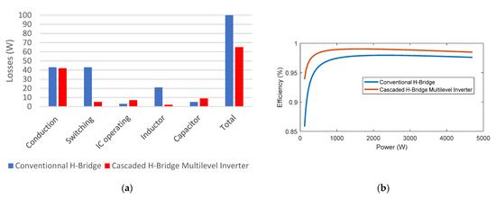
Figure 7.
(a) Losses distribution comparison at maximum output power (b) Efficiency comparison.
The efficiency of both converters in the function of the total output power is shown in Figure 7b. The CHBMLI has better efficiency than the conventional H-Bridge for any output power. Overall, the key factors that contribute to the better efficiency of the CHBMLI are reduced switching and inductor losses. The reduced losses both come from the low switching voltages of the CHBMLI due to its multilevel ability. At low output power (<100 W), the efficiencies of both converters are affected by their IC operating losses because they remain constant regardless of the output power. As the power increases, the efficiency increases as well because the IC operating losses become negligible. Around 1500 W, both converters reach their peak efficiencies: 98.2% for the conventional H-Bridge and 99% for the CHBMLI. From that point, efficiencies decrease due to conduction and inductor losses. Indeed, unlike other losses, they are proportional to (when is proportional to ). At 4700 W, the efficiency of the conventional H-Bridge is 97.9%, and the efficiency of the CHBMLI is 98.4%. For any output power, the efficiency of the CHBMLI is at least superior to the efficiency of the conventional H-Bridge by 0.5%.
4.4. MOSFETs
4.4.1. Temperature Rise
Limiting the temperature rise is then a trade-off between the size and cost of the heatsink and MOSFETs lifespan and losses. A proper comparison of the transistors must be made by considering the same temperature rise. The losses per transistor in both topologies are:
First, for the CHBMLI with maximum output power, the temperature rise of each transistor without any heatsink is:
where is the junction-to-ambient thermal resistance (). In a converter design, the junction temperature of a transistor is usually limited to 100 °C. A 36 °C temperature rise at maximum output power is perfectly acceptable for a solar inverter. No heatsink is required for the CHBMLI. For the conventional H-Bridge with maximum output power, the temperature rise of each transistor without any heatsink is:
This high temperature rise is caused by complete losses distributed on a reduced number of transistors. On top of that, due to lower efficiency, the total transistors losses are higher for the conventional H-Bridge. Finally, compared to the CHBMLI, each transistor dissipates significantly more energy. In this case, a heatsink is required. We chose to use a single heatsink on which all the transistors are fixed. The value of the heatsink is calculated to limit the junction temperature to , which means a temperature rise of 75 °C from an ambient temperature of 25 °C:
where is the junction-to-case thermal resistance (), is the case-to-heatsink thermal resistance () and is the required heatsink thermal resistance (K/W).
Then:
Thus:
The chosen heatsink is a 0.6 K/W heatsink from ABL components (109AB1500B, $14).
4.4.2. Gate Drivers
The selected MOSFET drivers for the conventional H-Bridge are two UCC21520 Isolated Dual-Channel Gate Drivers. These drivers are designed to power MOSFETs with a very low propagation delay (typically 19 ns) and a high common-mode transient immunity (up to 100 V/ns). On each driver, both channels are fully isolated and are guaranteed to operate with a DC voltage up to 1500 V.
For the CHBMLI, a unique H-bridge driver is used: the MIC4606. This driver also has a very low propagation delay (typically 35 ns) and very low power consumption. It uses a bootstrap circuit to supply the two high-side transistors per H-Bridge up to a maximal voltage of 80 V. Those drivers do not need to be isolated because they are directly powered by the solar panel (through a small local power supply).
4.4.3. Overall Cost
The overall cost for the MOSFETs (including the drivers and the heatsink) is presented in Table 10. The CHBMLI uses N times more transistors than the conventional H-Bridge. However, those transistors are much cheaper due to their low voltage characteristics and compact packages. The addition of drivers (more expensive for the CHBMLI) makes the cost (MOSFETs + driver) similar between the two topologies. In the end, the need for a heatsink for the conventional H-Bridge leads to a higher overall cost (for the MOSFETs part) than for the CHBMLI.
Table 10.
MOSFETs + Driver + Heatsink.
This paragraph does not take into account the cost of the other components in the complete converter (AOP for measurements, microcontroller, onboard power supply). It is expected that, when adding the total cost of every component of the circuit, the CHBMLI might not keep its advantage.
4.5. Summary
All the comparison points of this section are summed up in Table 11.
Table 11.
Summary of comparison points between both topologies.
5. Experimental Measurements for the CHBMLI
The objective of this section is to validate the thermal design of the CHBMLI through a temperature measurement on a real prototype. Only the CHBMLI prototype was built to limit the time and resources required. Furthermore, due to limited equipment, this validation is performed by measuring the efficiency and temperature of a single module operating at its rated power (365 W). For this purpose, a sinusoidal four-quadrant power supply (TOE7610) is used on the output, while a DC power source (Cpx400D) is used on the input. On the other hand, a prototype composed of eight modules used at a lower power is tested to provide the inverter waveforms, such as the inverter voltage , the module output voltage and the output grid current .
The control of the converter was detailed in previous work by the authors. First, it was demonstrated that it is possible to control the CHBMLI with a hardware architecture having up to 20 modules with a switching frequency of 20 kHz [36]. A second paper detailed how this topology can be controlled with a reduced number of sensors [23] while operating, for each solar panel, an individual Maximum Power Point Tracking (MPPT) algorithm with minimum power oscillations. Those papers demonstrate that the CHBMLI can be controlled with low-cost components while maintaining a wide range of operations (number of modules > 20).
5.1. Experimental Setup
The experimental setup for the CHBMLI is presented in Figure 8. Figure 8a presents the prototype of the CHBMLI with 8 H-Bridge modules with all the output placed in series, Figure 8b presents the master controller of the inverter with the main MCU (STM32F446RE), and Figure 8c presents the circuit with isolated AC voltage and current sensors and relays to connect the inverter to the grid. This setup was designed according to the elements detailed in Section 3.
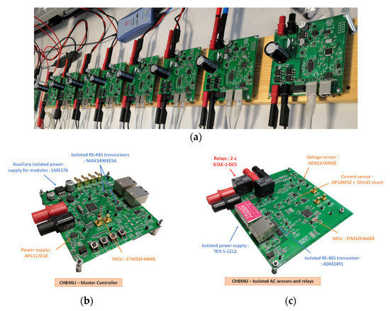
Figure 8.
(a) Experimental setup of the Cascaded H-Bridge Multilevel Inverter with eight modules (b) Master controller of the CHBMLI (c) Circuit with isolated AC sensors and relays for the CHBMLI.
5.2. Temperature Rise of a Single Module (CHBMLI)
A single module is detailed in Figure 9a. The left side of the board contains the power converter (H-Bridge and capacitors). Under an input power of 365 W and a switching frequency of 1.5 kHz (for the H-Bridge of this module), the power switches have a temperature rise of 32 °C (Figure 9b), which validates the thermal analysis presented in Section 4.4. The measured efficiency (including IC operating losses) is 98.5%. This measurement does not include inductor losses. However, with a full converter at nominal power, the low inductance value would not significantly modify the overall efficiency. This low temperature rise confirms that no heatsink is required to maintain the junction temperature of the MOSFETs below 100 °C. On top of that, in a conventional inverter, the heat released by the MOSFETs (with heatsink) usually increases the temperature of the DC-link capacitors, which have to be placed close to the H-Bridge in order to reduce the parasitic inductance of the track. This temperature rise of the DC-link capacitor often leads to faster aging and reduced lifetime [38]. Failure of the aluminum electrolytic of the DC-link capacitor is one of the most common faults on a conventional H-bridge.
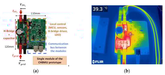
Figure 9.
(a) Prototype of a single module of the Cascaded H-Bridge Multilevel Inverter (CHBMLI) (b) Thermal image of a module at .
5.3. Waveforms of the CHBMLI
The waveform of the CHBMLI voltage (in red) and the output current (in blue) are shown in Figure 10a. This figure is zoomed over a half grid period in Figure 10b, including in green the output voltage of a single module. The low switching frequency (in green) of a single module (compared to the high switching frequency of the complete converter) can be observed.
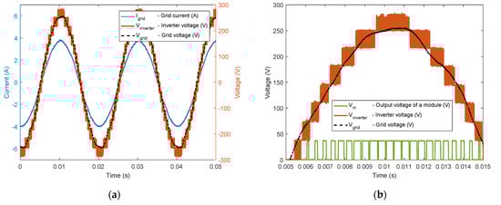
Figure 10.
(a) Waveforms of the CHBMLI with , , : Current grid (blue), Inverter Voltage (red), Grid voltage (black) (b) Same as (a) but including the output voltage of a single module (green).
Due to limited power on the experimental setup, the complete converter was tested with 70 W per module. This results in an output RMS current of 3 A, and an off-the-shelf inductor was chosen for this current (2 mH/5 A) to limit the harmonics. For the same output current, a high-frequency ripple, a bigger inductor would be required (by a factor ). The output sinusoidal current (in blue) is set in phase with the grid voltage (in black) in order to ensure a unity power factor. On top of that, each solar panel is regulated around its own optimal voltage (). Thus, the energy extraction is maximized by the CHBMLI. Under partially shaded weather conditions, the CHBMLI extracts more power than the conventional H-Bridge.
6. Conclusions
A comparison between the design of the conventional H-Bridge and the CHBMLI is presented in this paper. First, a series of constraints regarding the efficiency, the maximum solar power extraction, the components’ lifespan, and the cost were established to make the comparison as realistic as possible. For both topologies, inductors, capacitors, transistors, and heatsink are sized. The multilevel ability of the CHBMLI makes it more interesting when it comes to filtering the output current of the inverter, thus reducing the size and cost of the inductor. As both topologies are DC−AC converters with the same amount of DC and AC power and considering the same DC-link voltage ripple ratio, the capacitor’s energy sizing is similar in both cases. For the conventional H-Bridge, low-value and medium-voltage capacitors are used, and for the CHBMLI, medium-value and low-voltage capacitors are used. The reduced choices for capacitors for the CHBMLI lead to higher global ESR, which creates slightly higher losses. When it comes to global efficiency, the CHBMLI has a serious advantage due to very low switching losses compared to the conventional H-Bridge, thanks to low voltage levels. The reduced losses, which are furthermore spread over a higher number of transistors, lead to low temperature rise without the need for a heatsink for the CHBMLI. For the conventional H-Bridge, the trade-off between cost and efficiency leads to the use of a heatsink to cool transistors. The vast choice of small voltage transistors (for the CHBMLI), despite the large number of transistors required, makes it easier to select low-cost components for the design. The cost of medium voltage transistors combined with the cost of the heatsink and the isolated drivers is about 50% superior to the cost of transistors and the drivers for the CHBMLI with the same performances (same global conduction losses and same temperature rise). A real CHBMLI prototype with eight modules was built to validate several aspects of the design. The converter was tested with a 20 kHz switching frequency on the grid voltage with a sinusoidal output current of 3 Arms, a low current ripple, and a unity power factor. The low temperature rise (without a heatsink) of a single module at 365 W was also validated.
Author Contributions
Conceptualization, T.B., G.D. and R.T.; methodology, T.B., G.D. and R.T.; software, T.B.; validation, T.B.; formal analysis, T.B., G.D. and R.T.; investigation, T.B.; resources, T.B.; writing—original draft preparation, T.B.; writing—review and editing, T.B., G.D. and R.T. All authors have read and agreed to the published version of the manuscript.
Funding
This research received no external funding.
Conflicts of Interest
The authors declare no conflict of interest.
References
- Ayadi, F.; Colak, I.; Garip, I.; Bulbul, H.I. Targets of Countries in Renewable Energy. In Proceedings of the 2020 9th International Conference on Renewable Energy Research and Application (ICRERA), Glasgow, UK, 27 September 2020; IEEE: Piscataway, NJ, USA, 2020; pp. 394–398. [Google Scholar]
- Kaizuka, I.; Yamaya, H.; Ohigashi, T.; Kurihara, R.; Ikki, O. Cost Analysis and Cost Reduction Opportunities of Residential PV System in the Japan. In Proceedings of the 2017 IEEE 44th Photovoltaic Specialist Conference (PVSC), Washington, DC, USA, 25–30 June 2017; IEEE: Piscataway, NJ, USA, 2017; pp. 2159–2162. [Google Scholar]
- Alluhaybi, K.; Batarseh, I.; Hu, H. Comprehensive Review and Comparison of Single-Phase Grid-Tied Photovoltaic Microinverters. IEEE J. Emerg. Sel. Top. Power Electron. 2020, 8, 1310–1329. [Google Scholar] [CrossRef]
- Bhattacharjee, A.K.; Kutkut, N.; Batarseh, I. Review of Multiport Converters for Solar and Energy Storage Integration. IEEE Trans. Power Electron. 2019, 34, 1431–1445. [Google Scholar] [CrossRef]
- Deshpande, S.; Bhasme, N.R. A Review of Topologies of Inverter for Grid Connected PV Systems. In Proceedings of the 2017 Innovations in Power and Advanced Computing Technologies (i-PACT), Vellore, India, 21–22 April 2017; IEEE: Piscataway, NJ, USA, 2017; pp. 1–6. [Google Scholar]
- Dreher, J.R.; Marangoni, F.; Schuch, L.; Martins, M.L.D.S.; Della Flora, L. Comparison of H-Bridge Single-Phase Transformerless PV String Inverters. In Proceedings of the 2012 10th IEEE/IAS International Conference on Industry Applications, Fortaleza, CE, Brazil, 5–7 November 2012; IEEE: Piscataway, NJ, USA, 2012; pp. 1–8. [Google Scholar]
- Filho, F.; Cao, Y.; Tolbert, L.M. 11-Level Cascaded H-Bridge Grid-Tied Inverter Interface with Solar Panels. In Proceedings of the 2010 Twenty-Fifth Annual IEEE Applied Power Electronics Conference and Exposition (APEC), Palm Springs, CA, USA, 21–25 February 2010; IEEE: Piscataway, NJ, USA, 2010; pp. 968–972. [Google Scholar]
- Cha, H.; Vu, T.-K.; Kim, J.-E. Design and Control of Proportional-Resonant Controller Based Photovoltaic Power Conditioning System. In Proceedings of the 2009 IEEE Energy Conversion Congress and Exposition, San Jose, CA, USA, 20–24 September 2009; IEEE: Piscataway, NJ, USA, 2009; pp. 2198–2205. [Google Scholar]
- Joshi, M.; Shoubaki, E.; Amarin, R.; Modick, B.; Enslin, J. A High-Efficiency Resonant Solar Micro-Inverter. In Proceedings of the 2011 14th European Conference on Power Electronics and Applications, Birmingham, UK, 30 August–1 September 2011; IEEE: Piscataway, NJ, USA, 2011; p. 10. [Google Scholar]
- Musavi, F. A High-Performance Cost-Effective Resonant Converter with a Wide Input Range in Solar Power Applications. In Proceedings of the 2018 IEEE Energy Conversion Congress and Exposition (ECCE), Portland, OR, USA, 23–27 September 2018; IEEE: Piscataway, NJ, USA, 2018; pp. 4756–4759. [Google Scholar]
- Xiao, B.; Filho, F.; Tolbert, L.M. Single-Phase Cascaded H-Bridge Multilevel Inverter with Nonactive Power Compensation for Grid-Connected Photovoltaic Generators. In Proceedings of the 2011 IEEE Energy Conversion Congress and Exposition, Phoenix, AZ, USA, 17–22 September 2011; IEEE: Piscataway, NJ, USA, 2011; pp. 2733–2737. [Google Scholar]
- Xiao, B.; Shen, K.; Mei, J.; Filho, F.; Tolbert, L.M. Control of Cascaded H-Bridge Multilevel Inverter with Individual MPPT for Grid-Connected Photovoltaic Generators. In Proceedings of the 2012 IEEE Energy Conversion Congress and Exposition (ECCE), Raleigh, NC, USA, 15–20 September 2012; IEEE: Piscataway, NJ, USA, 2012; pp. 3715–3721. [Google Scholar]
- Xiao, B.; Hang, L.; Mei, J.; Riley, C.; Tolbert, L.M.; Ozpineci, B. Modular Cascaded H-Bridge Multilevel PV Inverter With Distributed MPPT for Grid-Connected Applications. IEEE Trans. Ind. Applicat. 2015, 51, 1722–1731. [Google Scholar] [CrossRef]
- Biswas, M.M.; Podder, S.; Khan, M.Z.R. Modified H-Bridge Multilevel Inverter for Photovoltaic Micro-Grid Systems. In Proceedings of the 2016 9th International Conference on Electrical and Computer Engineering (ICECE), Dhaka, Bangladesh, 20–22 December 2016; IEEE: Piscataway, NJ, USA, 2016; pp. 377–380. [Google Scholar]
- Nirmal Mukundan, C.M.; Jayaprakash, P. Cascaded H-Bridge Multilevel Inverter Based Grid Integration of Solar Power with PQ Improvement. In Proceedings of the 2018 IEEE International Conference on Power Electronics, Drives and Energy Systems (PEDES), Chennai, India, 18–21 December 2018; IEEE: Piscataway, NJ, USA, 2018; pp. 1–6. [Google Scholar]
- Esram, T.; Chapman, P.L. Comparison of Photovoltaic Array Maximum Power Point Tracking Techniques. IEEE Trans. Energy Convers. 2007, 22, 439–449. [Google Scholar] [CrossRef]
- Subudhi, B.; Pradhan, R. A Comparative Study on Maximum Power Point Tracking Techniques for Photovoltaic Power Systems. IEEE Trans. Sustain. Energy 2013, 4, 89–98. [Google Scholar] [CrossRef]
- Femia, N.; Petrone, G.; Spagnuolo, G.; Vitelli, M. Optimization of Perturb and Observe Maximum Power Point Tracking Method. IEEE Trans. Power Electron. 2005, 20, 963–973. [Google Scholar] [CrossRef]
- Shahabadini, M.; Iman-Eini, H. Leakage Current Suppression in Multilevel Cascaded H-Bridge Based Photovoltaic Inverters. IEEE Trans. Power Electron. 2021, 36, 13754–13762. [Google Scholar] [CrossRef]
- Villanueva, E.; Correa, P.; Rodriguez, J.; Pacas, M. Control of a Single-Phase Cascaded H-Bridge Multilevel Inverter for Grid-Connected Photovoltaic Systems. IEEE Trans. Ind. Electron. 2009, 56, 4399–4406. [Google Scholar] [CrossRef]
- Khan, R.A.; Farooqui, S.A.; Sarwar, M.I.; Ahmad, S.; Tariq, M.; Sarwar, A.; Zaid, M.; Ahmad, S.; Shah Noor Mohamed, A. Archimedes Optimization Algorithm Based Selective Harmonic Elimination in a Cascaded H-Bridge Multilevel Inverter. Sustainability 2021, 14, 310. [Google Scholar] [CrossRef]
- Chavarria, J.; Biel, D.; Guinjoan, F.; Meza, C.; Negroni, J.J. Energy-Balance Control of PV Cascaded Multilevel Grid-Connected Inverters Under Level-Shifted and Phase-Shifted PWMs. IEEE Trans. Ind. Electron. 2013, 60, 98–111. [Google Scholar] [CrossRef]
- Bertin, T.; Despesse, G.; Thomas, R. Current Sensorless Individual MPPT Control on a Cascaded H-Bridge Multilevel Inverter. In Proceedings of the 2022 IEEE 20th International Power Electronics and Motion Control Conference (PEMC), Brasov, Romania, 25 September 2022; IEEE: Piscataway, NJ, USA, 2022; pp. 182–188. [Google Scholar]
- Pan, Y.; Zhang, C.; Yuan, S.; Chen, A.; He, J. A Decentralized Control Method for Series Connected PV Battery Hybrid Microgrid. In Proceedings of the 2017 IEEE Transportation Electrification Conference and Expo, Asia-Pacific (ITEC Asia-Pacific), Harbin, China, 7–10 August 2017; IEEE: Piscataway, NJ, USA, 2017; pp. 1–6. [Google Scholar]
- Zhang, X.; Hu, Y.; Mao, W.; Zhao, T.; Wang, M.; Liu, F.; Cao, R. A Grid-Supporting Strategy for Cascaded H-Bridge PV Converter Using VSG Algorithm With Modular Active Power Reserve. IEEE Trans. Ind. Electron. 2021, 68, 186–197. [Google Scholar] [CrossRef]
- Krein, P.T.; Balog, R.S.; Mirjafari, M. Minimum Energy and Capacitance Requirements for Single-Phase Inverters and Rectifiers Using a Ripple Port. IEEE Trans. Power Electron. 2012, 27, 4690–4698. [Google Scholar] [CrossRef]
- Aluminum Electrolytic Capacitors—General Technical Information. Available online: https://docs.rs-online.com/3570/0900766b815c4ec7.pdf (accessed on 16 April 2023).
- Cha, H.; Vu, T.-K. Comparative Analysis of Low-Pass Output Filter for Single-Phase Grid-Connected Photovoltaic Inverter. In Proceedings of the 2010 Twenty-Fifth Annual IEEE Applied Power Electronics Conference and Exposition (APEC), Palm Springs, CA, USA, 21–25 February 2010; pp. 1659–1665. [Google Scholar]
- Kim, H.; Kim, K.-H. Filter Design for Grid Connected PV Inverters. In Proceedings of the 2008 IEEE International Conference on Sustainable Energy Technologies, Singapore, 24–27 November 2008; IEEE: Piscataway, NJ, USA, 2008; pp. 1070–1075. [Google Scholar]
- Ferroxcube Data Handbook 2013. Available online: https://www.ferroxcube.com/en-global/download/download/11 (accessed on 16 April 2023).
- Ayachit, A.; Kazimierczuk, M.K. Thermal Effects on Inductor Winding Resistance at High Frequencies. IEEE Magn. Lett. 2013, 4, 0500304. [Google Scholar] [CrossRef]
- Kandeel, Y.M.; Orabi, M.; El-Nemr, M.K.; Youssef, M. Prediction of Inductor AC Power Loss in PSiP Buck Converter Based on Steinmetz Parameters. In Proceedings of the 2014 IEEE 36th International Telecommunications Energy Conference (INTELEC), Vancouver, BC, USA, 28 September–2 October 2014; IEEE: Piscataway, NJ, USA, 2014; pp. 1–8. [Google Scholar]
- Graovac, D.D.; Pürschel, M.; Kiep, A. MOSFET Power Losses Calculation Using the Data—Sheet Parameters. Infineon Appl. Note 2006, 1, 1–23. [Google Scholar]
- Guo, J.; Ge, H.; Ye, J.; Emadi, A. Improved Method for MOSFET Voltage Rise-Time and Fall-Time Estimation in Inverter Switching Loss Calculation. In Proceedings of the 2015 IEEE Transportation Electrification Conference and Expo (ITEC), Dearborn, MI, USA, 14–17 June 2015; IEEE: Piscataway, NJ, USA, 2015; pp. 1–6. [Google Scholar]
- Sahoo, S.K.; Bhattacharya, T. Phase-Shifted Carrier-Based Synchronized Sinusoidal PWM Techniques for a Cascaded H-Bridge Multilevel Inverter. IEEE Trans. Power Electron. 2018, 33, 513–524. [Google Scholar] [CrossRef]
- Bertin, T.; Despesse, G.; Thomas, R. Cascaded H-Bridge Multilevel Inverter with a Distributed Control System for Solar Applications. In Proceedings of the 2022 Smart Systems Integration (SSI), Grenoble, France, 26–28 April 2022; IEEE: Piscataway, NJ, USA, 2022; pp. 1–4. [Google Scholar]
- Kjaer, S.B.; Pedersen, J.K.; Blaabjerg, F. A Review of Single-Phase Grid-Connected Inverters for Photovoltaic Modules. IEEE Trans. Ind. Applicat. 2005, 41, 1292–1306. [Google Scholar] [CrossRef]
- Yao, K.; Cao, C.; Yang, S. Noninvasive Online Condition Monitoring of Output Capacitor’s ESR and C for a Flyback Converter. IEEE Trans. Instrum. Meas. 2017, 66, 3190–3199. [Google Scholar] [CrossRef]


Disclaimer/Publisher’s Note: The statements, opinions and data contained in all publications are solely those of the individual author(s) and contributor(s) and not of MDPI and/or the editor(s). MDPI and/or the editor(s) disclaim responsibility for any injury to people or property resulting from any ideas, methods, instructions or products referred to in the content. |
© 2023 by the authors. Licensee MDPI, Basel, Switzerland. This article is an open access article distributed under the terms and conditions of the Creative Commons Attribution (CC BY) license (https://creativecommons.org/licenses/by/4.0/).