1. Introduction
The sensors market is constantly growing and is expected to reach USD 42.1 billion by 2029 for industrial sensors alone [
1]. Also, the new strategy of the European Union, the European Green Deal [
2], strengthens the growing European interest in a sustainable industry in terms of energy and clean environment. Energy harvesting is the process of collecting a small amount of energy from the environment. It offers a solution to this sustainability problem; by harvesting environmental energy, we should be able to respond to the energy shortage by replacing polluting power supplies, such as batteries, or at least to increase their life span. Another motivation could be the fact that the growing demand for safe, power efficient, and durable systems requiring minimal or no maintenance has resulted in an expanding energy harvesting system market; the value of this market is expected to reach USD 0.9 billion by 2028 [
3].
The main energy sources found in the environment are the following: solar, aeolian, acoustic, mechanical vibration, and thermoelectrical. The energy coming from mechanical vibrations could be harvested using four mechanisms: electrostatic, electromagnetic, magneto-strictive, and piezoelectric [
4].
In particular, piezoelectric energy harvesters can offer the ability to meet application requirements such as high efficiency in energy conversion and compatibility for miniaturization. Their purpose is to “harvest” mechanical energy, in our case environmental vibrations, which induce strain in the piezoelectric layer, and, due to the direct piezoelectric effect, are converted into electrical energy. One of the best and most-used piezoelectric materials is PZT (lead zirconate titanate) but, in order to be in line with the European strategy, we have to choose a lead-free material for the piezoelectric layer.
Several piezoelectric lead-free materials were taken into account for the fabrication of the energy harvester, such as zinc oxide (ZnO), aluminum nitrate (AlN) or potassium sodium niobate (KNN). ZnO was successfully used by C.T. Pan et al. [
5] and Y. Li et al. [
6] in developing piezoelectric energy harvesters. Also, I. Kanno et al. [
7] and S.S. Won et al. [
8] successfully used KNN in developing energy harvesters. However, our preliminary tests have shown that it will be difficult to integrate these materials with our current technological capabilities. Therefore, we focused on using AlN-based piezoelectric materials.
AlN as a piezoelectric film in MEMS energy harvesters has been widely used, as can be seen in [
9]. For example, N. Jackson et al. evaluated three different designs of cantilever-based energy harvesters for low frequency usage, using the same piezoelectric film, AlN. They compared a wide beam, trapezoidal beam, and narrow beam structure resulting in a reported power density of 2.5, 0.78, and 0.65 mW/cm
3/g
2 at a resonant frequency of 149, 118, and 97 Hz, respectively. The acceleration was 0.2 g for the wide beam and 0.4 g for the other two [
10]. The authors also demonstrated an increase in the harvesting bandwidth by using an array of cantilevers. On a 4 cm
2 area, the bandwidth increased from 0.82 Hz to 26.4 Hz for an array of narrow beam cantilevers, from 0.9 Hz to 9 Hz for the trapezoidal ones, and from 1.2 Hz to 4.8 Hz for an array of wide beam cantilevers.
An array of cantilevers was also fabricated by J.-Q. Liu et al. [
11]. They used PZT as the piezoelectric material on a silicon cantilever with a nickel-proof mass and obtained an effective electrical power of 3.98 µW. The array consisted of three cantilevers with a resonant frequency between 226 Hz and 234 Hz. In order to overcome the different phases of cantilevers, which could diminish the effect of an array, the authors used a full-bridge rectifier after each cantilever and then connected them together.
Another array of cantilevers was fabricated by H. Yu et al. [
12] and X. Zhao et al. [
13]. They both used an array of five cantilevers connected together by a common silicon-proof mass. H. Yu used PZT as the piezoelectric material and obtained an output power of 66.75 µW at a resonant frequency of 234.5 Hz and an acceleration of 0.5 g. X. Zhao used AlN as the piezoelectric material and obtained 3.249 µW as the maximum generated power, at a resonant frequency of 230.4 Hz and an acceleration of 1 g.
In terms of improved AlN-based material, a significant increase in the generated energy is obtained by doping the AlN film with scandium (Sc) as S. Barth and others demonstrated [
14]. They measured a power of 350 µW for the Sc-doped AlN compared to 70 µW for pure AlN under optimum conditions.
The presented energy harvester consists of a double array of piezoelectric cantilevers fabricated using silicon-based MEMS technologies and Sc-doped AlN as a lead-free piezoelectric material. Sc-doped AlN is compatible with our technological capabilities and it has greater performance over the other materials presented above.
The purpose of the double array of cantilevers (2 × 10) is to obtain a larger output power magnitude for a bandwidth around the resonant frequency. The MEMS device includes 20 piezoelectric cantilevers which are designed as unimorph cantilevers and work in flexure mode with a resonant frequency in the environmental application domain (a few hundred Hz [
11]).
Regarding the device topology, we chose narrow beam cantilevers for a better chance of obtaining a bandwidth around the resonant frequency and a smaller area. Although the wide beam cantilever design is more efficient in terms of electrical power, as proven in [
15], it could take up a large area, especially when it comes to multiple cantilevers.
The MEMS device was successfully obtained on an area of 1 cm
2. Its resonant frequency is 465.2 Hz (measured with a laser Doppler interferometer) and the cantilevers were connected according to their phases. For an acceleration of 2 g RMS we obtained a stabilized output voltage of 1.8 V at the resonant frequency by using the integrated circuit LTC3588-1. A stabilized voltage of 1.8 V could easily be used to power a wide range of commercially available ultra-low-power microcontrollers, such as STMicroelectronics [
16], NXP Semiconductors [
17], or Texas Instruments [
18], and to intermittently collect data from sensor nodes.
2. Materials and Methods
The energy harvester device described in this paper is based on the direct piezoelectric effect, leading to direct transformation of mechanical energy into electrical energy. When a piezoelectric material is deformed or stressed, a voltage is generated across the material.
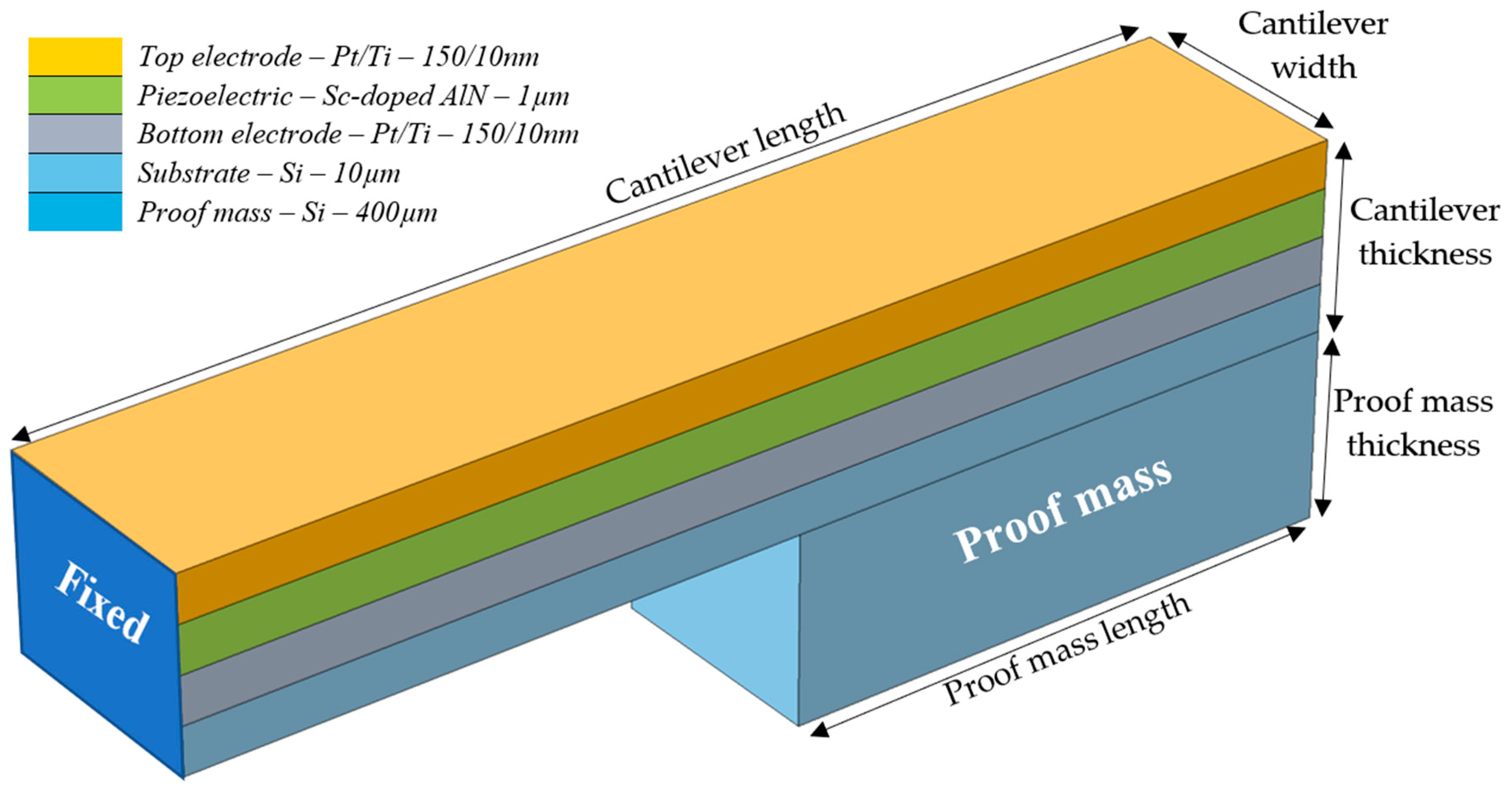
The purpose of the research work is to obtain a lead-free energy harvester for supplying inaccessible low-power sensors or sensor networks. It is based on a MEMS device with 20 piezoelectric harvesting cantilevers, designed as unimorph cantilevers working in flexure mode and with the 3–1 transversal mode as the electromechanical coupling mode (the electric field is produced on an axis orthogonally to the axis of applied stress). An overview of one piezoelectric cantilever is presented in
Figure 1. The flexure mode is the first mode of vibration and has the lowest resonant frequency. It also provides the largest deflection and therefore the largest amount of electrical energy. Adding a proof mass will further lower the resonant frequency to a resonant frequency closer to the physical vibration sources.
Several lead-free piezoelectric materials were studied for the device fabrication, such as KNN, nanostructured ZnO, AlN, and Sc-doped AlN. Due to the incompatibility of the KNN and nanostructured ZnO fabrication steps with our technology capabilities, we were unable to integrate these piezoelectric materials with our device. Between AlN and Sc-doped AlN we chose the latter because of its superior piezoelectric properties over the AlN [
10] and its very good compatibility with the silicon technology.
We focused on obtaining a double array of proof mass cantilevers for a resonant frequency in the environmental application domain (a few hundred Hz) and a chip area of only 1 cm2. An array of cantilevers could provide us with a bandwidth of frequencies from which we could collect energy from the environment but with the cost of power magnitude. Also, this design gives us the possibility to connect multiple cantilevers in a small area.
The resonant frequency could be described by the equation below, assuming the added mass on the tip is much larger than the mass of the beam itself and the stiffness is unaffected [
19]:
where
Yeq is the equivalent Young’s modulus,
t,
L and
W are the thickness, length and width of the cantilever beam and
mi and
mc are the mass of the proof mass and the cantilever mass, respectively. As can be seen, the resonant frequency is given by the materials’ properties and the geometric parameters. Once the materials are set, the geometric parameters (length, thickness, and proof mass) are used in order to tune the resonant frequency.
The chosen software for employing the finite element method (FEM) was COMSOL Multiphysics 5.2, out of several similar tools available to us, including Ansys 18.1 and CoventorWare 2014, which can provide similar results. The reasons for choosing this software lie both in the team’s greater experience with COMSOL and several key attributes. On the one hand, CoventorWare is an excellent simulation tool when used in conjunction with microfabrication technologies. Ansys, on the other hand, is an excellent FEM tool for engineering applications, offering a broad suite of software products that cover various engineering disciplines. However, COMSOL, focused on multiphysics simulations, is usually the main choice for academic applications, due to its seamless capabilities to simulate coupled phenomena.
Regarding the current modeling and simulation purpose, our intention was to analyze the physical behavior, to determine the main outputs and to maximize the device’s efficiency through optimization. COMSOL’s meshing options provided the authors with better options to integrate very high geometrical aspect ratios (the length of the cantilever is in the millimeter range, while the thickness of the metal layers only has a few hundred nanometers) without high computational costs.
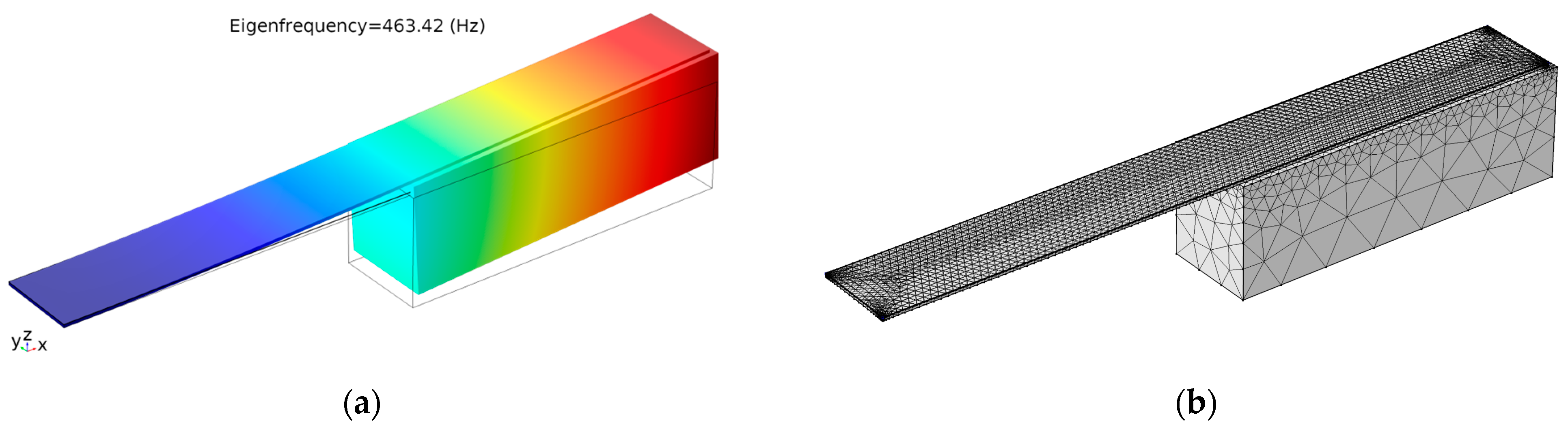
The simulation consists of a modal analysis for the eigenfrequencies, in order to determine the resonant frequency for the cantilever. The geometric parameters are as follows: a cantilever length of 2500 µm; a proof mass length of 1200 µm; a width of 300 µm for both parts, the cantilever and the proof mass; and a cantilever thickness of 10 µm. The thickness of the proof mass is 400 µm, the same as the thickness of the wafer. We obtained a resonant frequency for the first vibration mode (flexure mode) of around 460 Hz, as can be seen in
Figure 2a. For the simulation we used the materials described by
Figure 1, with their properties from the COMSOL library. We also took into account the effects of the DRIE process from the process flow resulting in a slightly larger proof mass (a width of 340 µm and a length of 1220 µm). The mesh consists of 61,487 domain elements, 23,042 boundary elements, and 1926 edge elements (
Figure 2b).
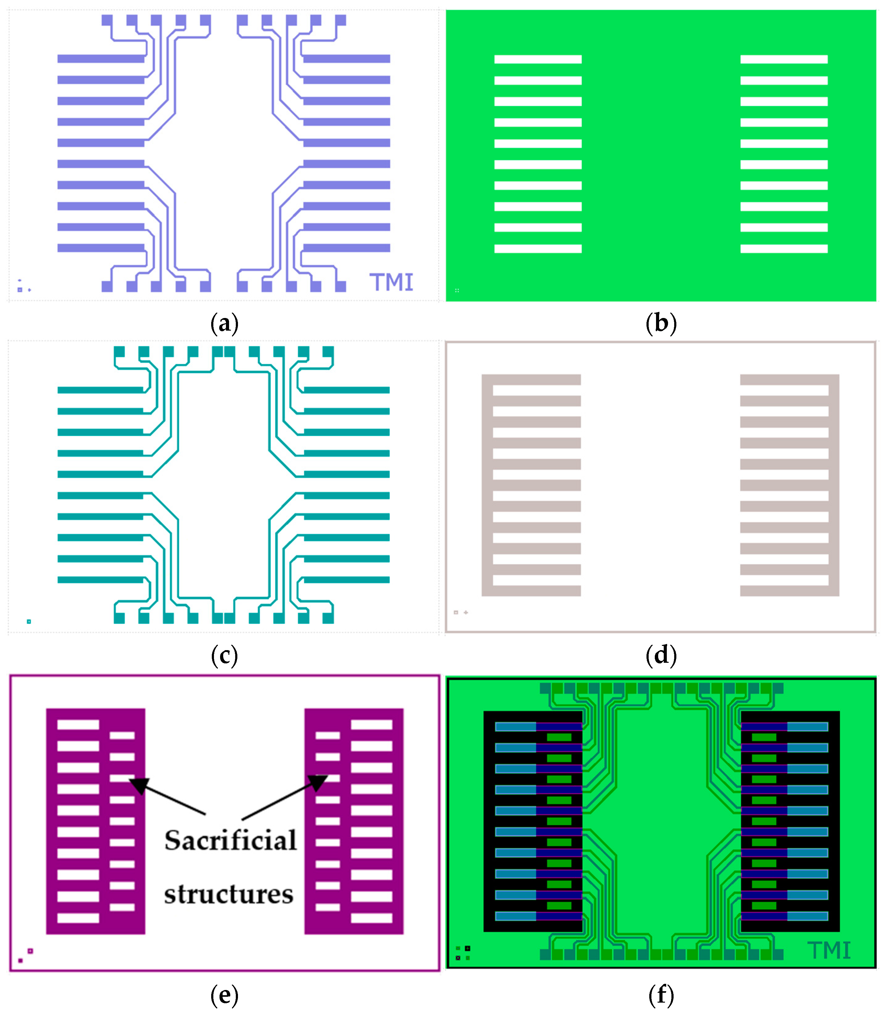
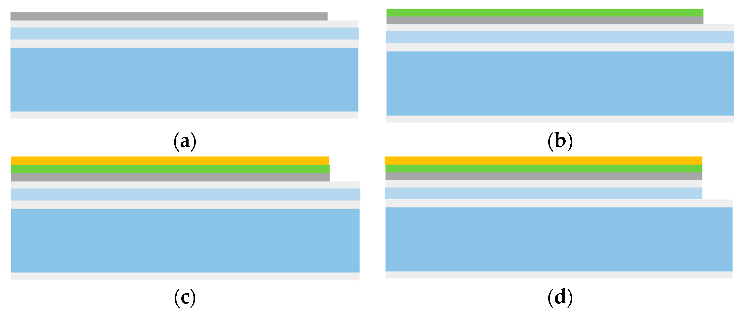
Using the geometric parameters from the simulation, we designed the fabrication masks (
Figure 3) and the process flow (
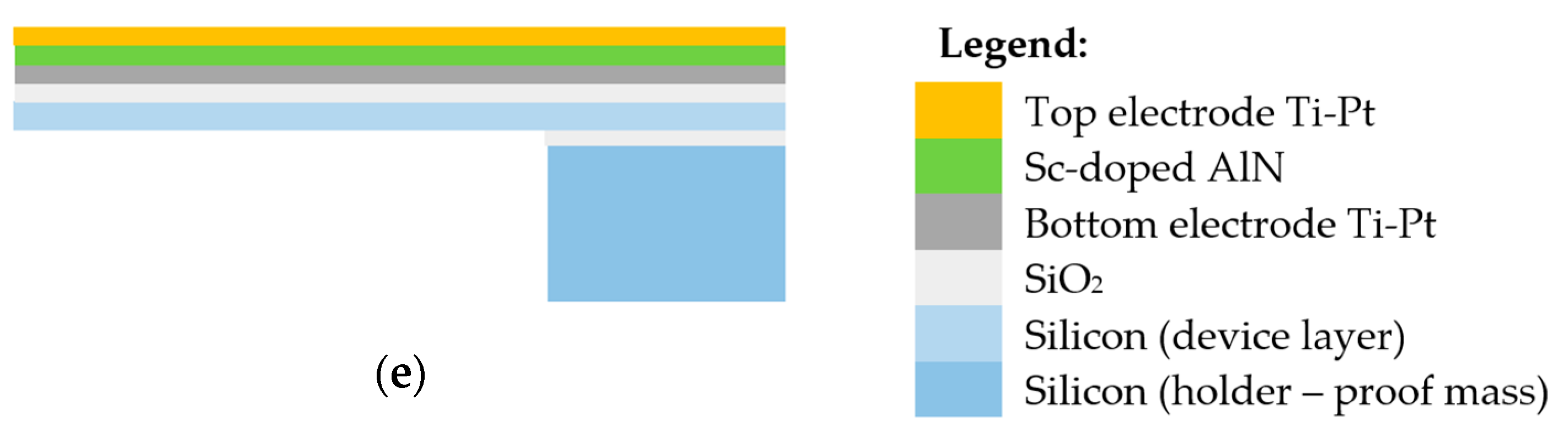
Figure 4). The process flow consists of five masks and deploys MEMS technologies for the fabrication of the energy harvester. It was designed for using only positive photoresists. The masks and process flow were fabricated by IMT-Bucharest, through IMT-MINAFAB, except for the piezoelectric layer which was provided by PIEMACS Sàrl (Lausanne, Switzerland).
The process starts with a SOI (silicon on insulator) wafer (device thickness of 10 µm, buried oxide of 500 nm and handler thickness of 400 µm) on which we thermally grew a silicon oxide layer of 500 nm. On top of the wafer, we deposited Ti-Pt (10–150 nm) by evaporation and patterned it by lift-off, resulting in the bottom electrode (
Figure 4a), using Mask 1 (
Figure 3a).
The next step is the deposition of the piezoelectric layer by RF sputtering (
Figure 4b) and its patterning using Mask 2 (
Figure 3b). The piezoelectric layer is 12% Sc-doped AlN and was possible thanks to PIEMACS Sàrl. The relative dielectric constant of the piezoelectric material is around 13 and its piezoelectric coefficient is around
e31,f = 1.3 C/m
2 [
20]. Also, the dielectric loss did not increase with Sc doping [
20].
The
Figure of Merit (FOM) could be described by the following equation [
21]:
The piezoelectric coefficient
d31 is determined using the known relation [
22]:
Equation (3) could be simplified as
s12 is negligible and hence we obtain the following:
where
Y is the Young’s modulus.
With a value of 150 GPa for Young’s modulus at a concentration of 12% for Sc [
14], we determine
d31 = 8.3 and a
FOM of 52.6 (dielectric loss 0.1).
The top electrode (
Figure 4c) is deposited as Ti-Pt (10–150 nm) by evaporation and patterned by lift-off using Mask 3 (
Figure 3c).
Mask 4 (
Figure 3d) is used to configure the cantilevers in the device layer of the SOI wafer by etching the silicon with a Bosch process of a deep reactive ion etching (DRIE) as shown in
Figure 4d.
The last step is to release the cantilevers by etching the back of the wafer using Mask 5 (
Figure 3e) and DRIE. The DRIE etch is stopped on the buried oxide layer. Afterwards, the buried oxide is etched using wet etching in a buffered hydrofluoric acid (BHF) solution and therefore the cantilevers are fully released (
Figure 4e). The distance between the cantilevers was designed at 300 µm to guarantee the silicon etching between the proof masses.
The DRIE process depends on the geometry of the mask. For small etching windows, like the space between the proof masses of the cantilevers, the etch rate is much lower than for big open etching windows, like near the base of the cantilevers, and the cantilevers will be fixed together. In order to make the etch rate uniform, we introduced some sacrificial structures between the cantilevers, as shown in
Figure 3e. These sacrificial structures were removed with the etching of the buried oxide. The overlayed masks are shown in
Figure 3f.
4. Discussion
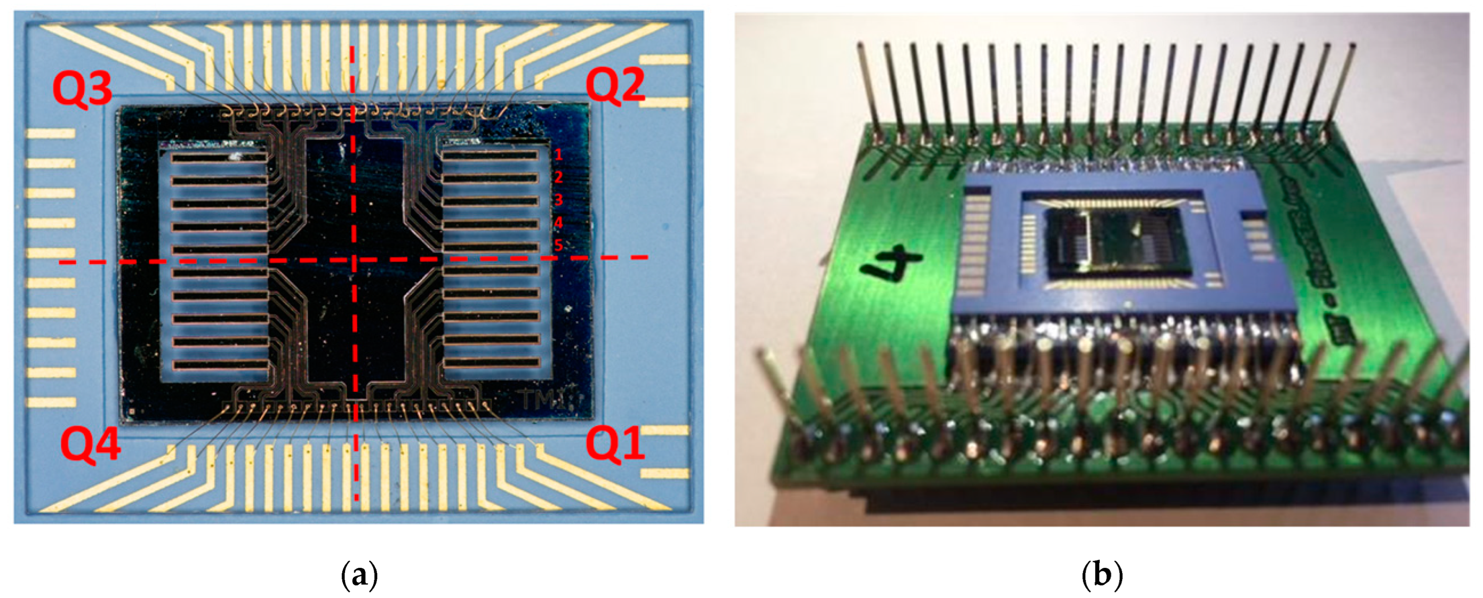
The piezoelectrical MEMS energy harvester with 2 × 10 piezoelectric cantilevers array was successfully fabricated and tested, and the resulting resonant frequency was ~465 Hz. The chip area was 1.02 cm2.
Sc-doped AlN has been chosen as the piezoelectric material because of its high performance and good compatibility with silicon-based technologies.
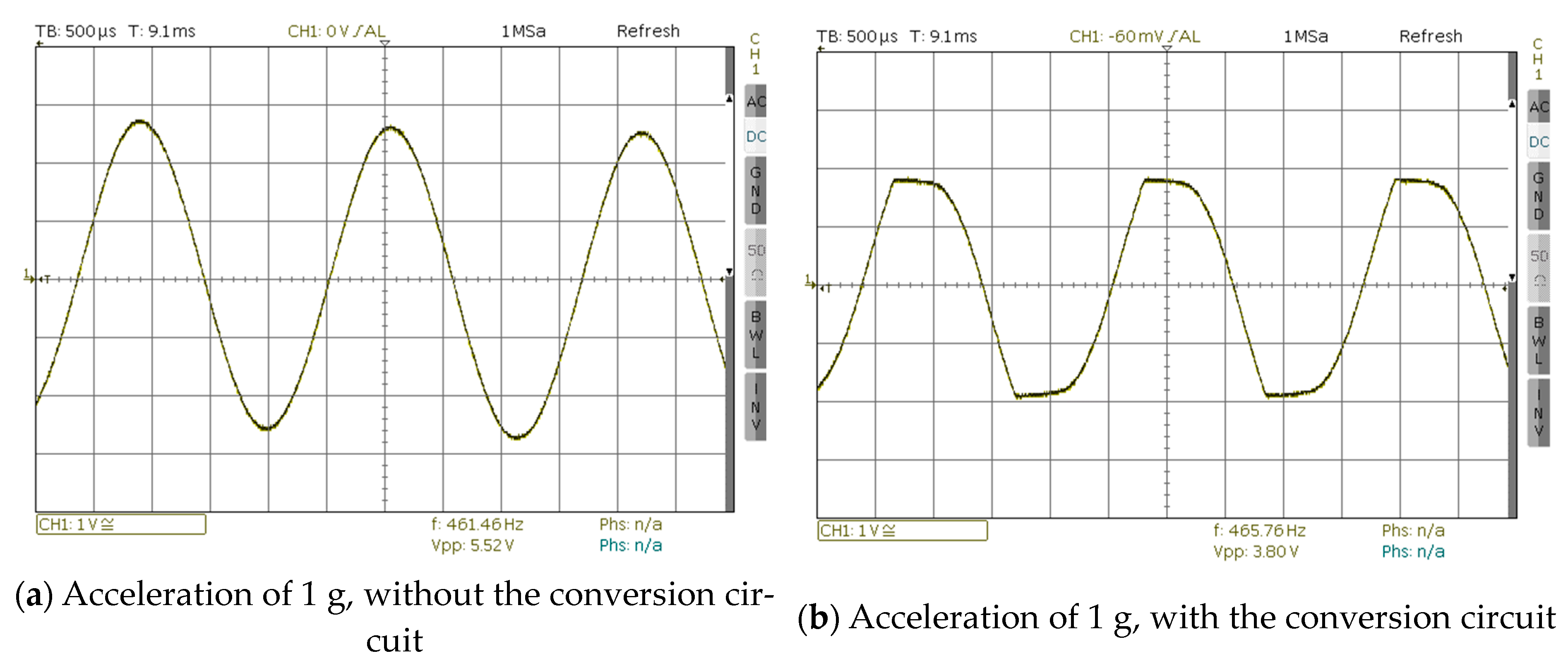
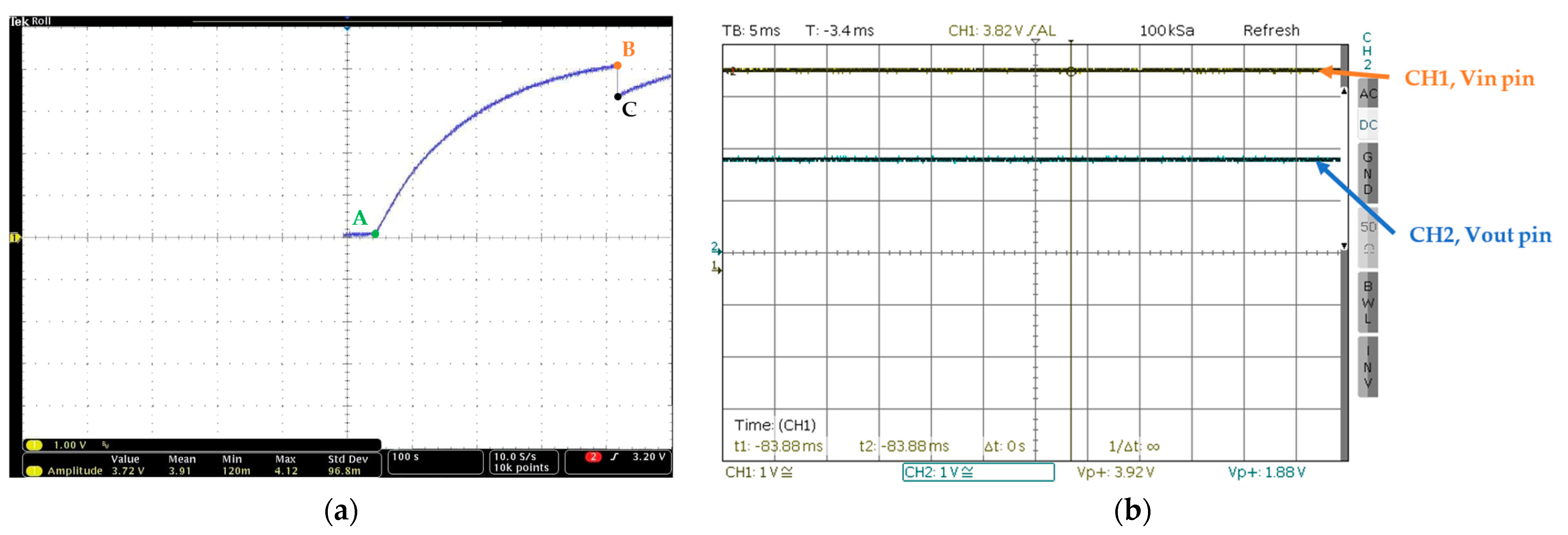
For the conversion circuit we chose the integrated circuit LTC3588-1, an off-the-shelf solution which is capable of offering various stabilized voltages, including 1.8 V. An experimental setup was built in order to test the MEMS devices at the desired frequencies, a setup which consists of a function generator, an oscilloscope, an audio amplifier, and a speaker.
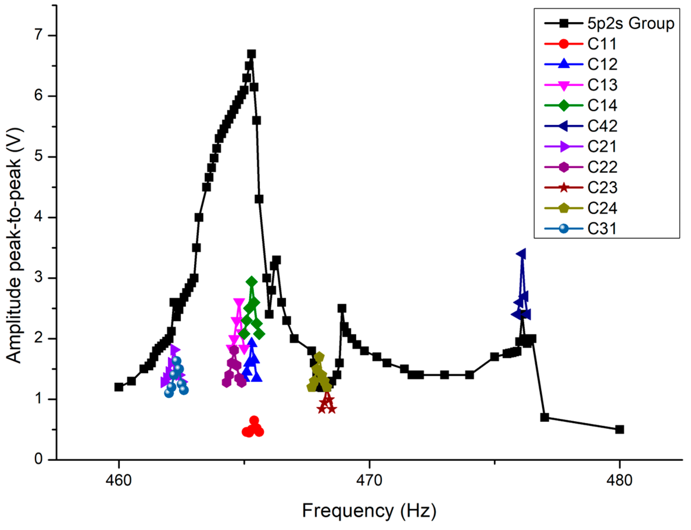
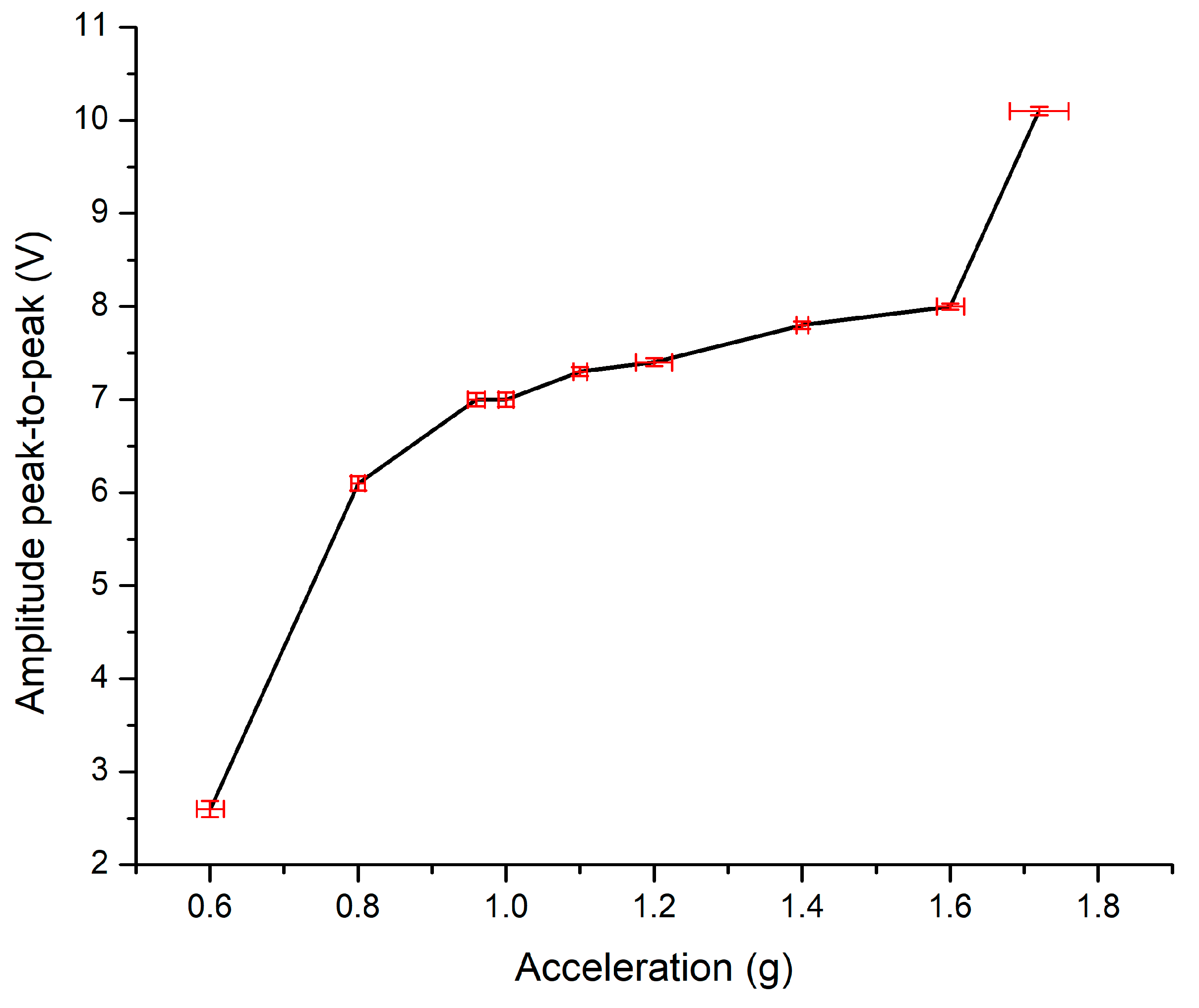
We obtained a stabilized output of 1.8 V at a resonant frequency of 465.2 Hz and an acceleration of 2 g RMS. The resonant frequency of 465.2 Hz is not for one cantilever but for the whole group, in this case, two branches in series with five cantilevers in parallel each.
The purpose of the cantilever array was to increase the frequency bandwidth from which we collect the ambient energy and, at the same time, to multiply the collected signal. We observed an improvement in the frequency bandwidth from which the device harvests the energy. This improvement was smaller than expected due to the unforeseen high values for the Q factor and the difficulty in phase-matching the cantilevers.
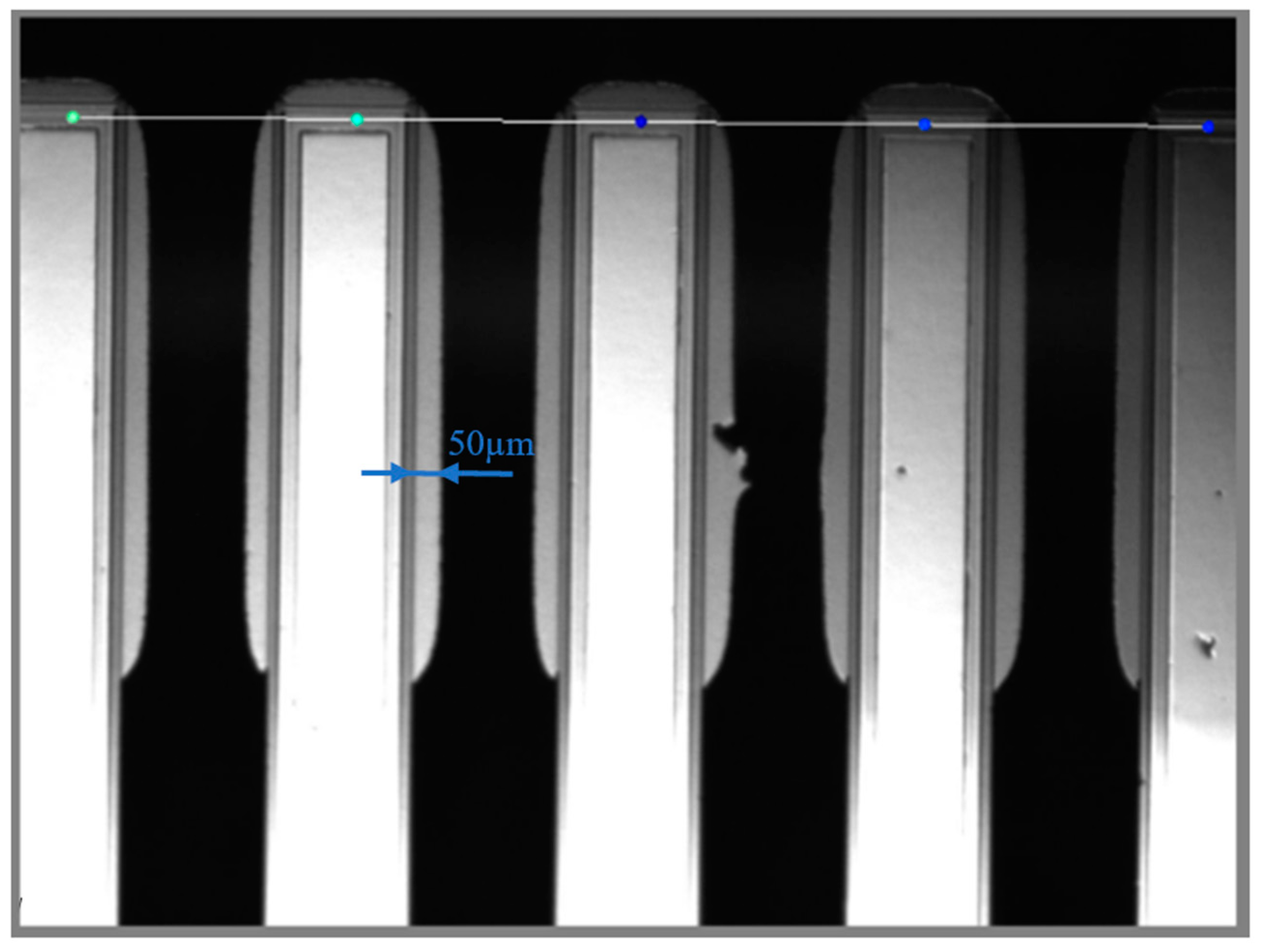
A challenge in the fabrication processes was the backside etching, etching which has to be performed through the whole wafer in order to configurate the proof masses of the cantilevers. It can be seen visually in
Figure 6, as well as in the measurements from
Table 1, that the etching process needs further optimization because of its variation, variation which can be observed in the small differences between the resonant frequencies and phases of the cantilevers. This variation is a drawback for the efficiency of the device because we could not use all the cantilevers from the same chip and we had to work with only half, connected together in 2 branches in series of 10 cantilevers in parallel each.
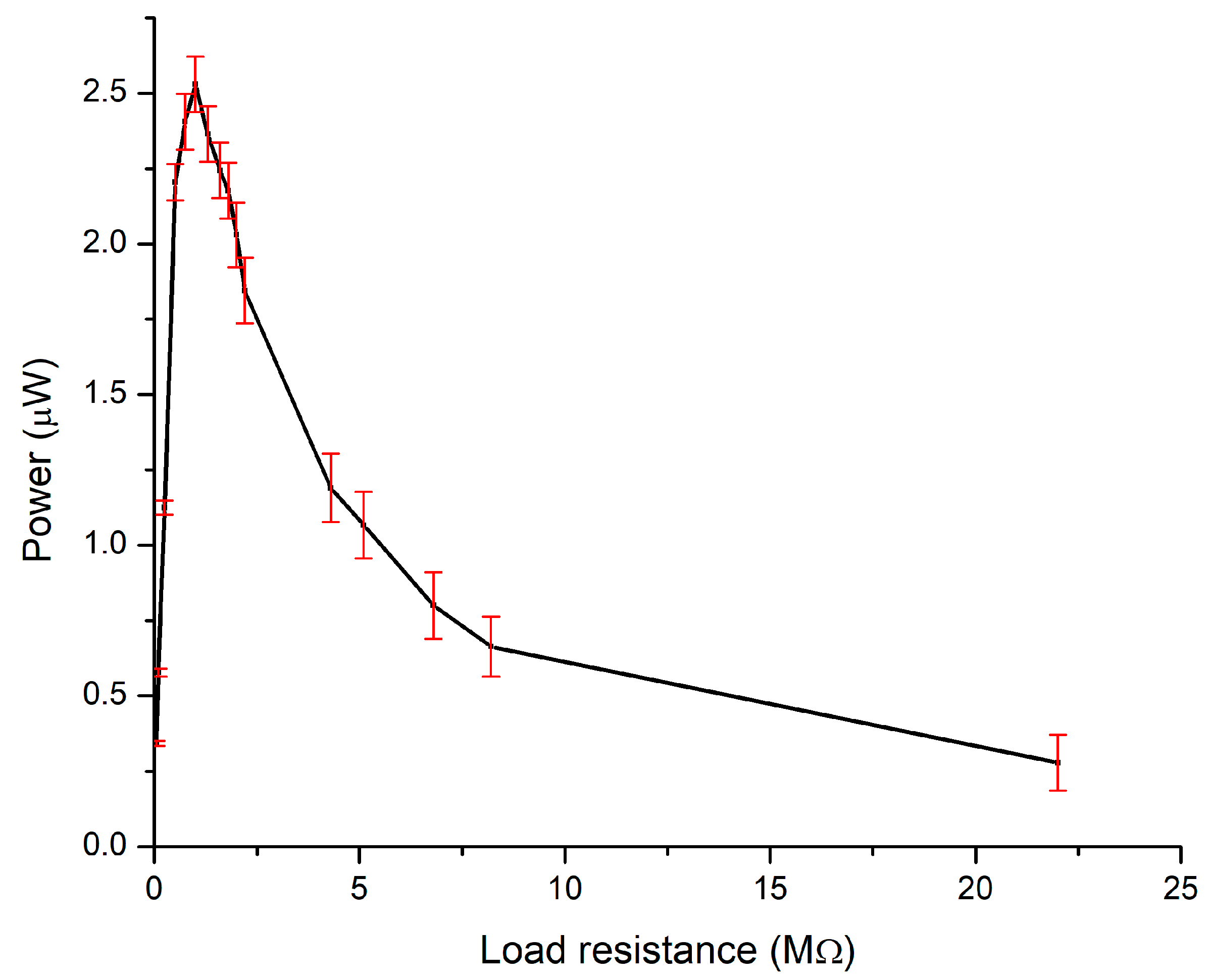
By itself, the device is capable of generating a power of 2.53 µW for an optimal load resistance of 1 MΩ, at an excitation of 1 g and a resonant frequency of 465.3 Hz. In this case, the normalized power density of the device is 0.215 µW/mm3/g2, for the unpacked device without the vibration volume. In order to take advantage of this, we would need to match this load resistance with the input impedance of the power circuitry which was not possible at this stage.
Comparing our device with others could be pretty difficult, as there are different designs, employment of different material or other factors. A common comparison factor is the power density normalized against acceleration squared, which includes information about the output power at an optimal resistance, at the resonant frequency, as well as the acceleration and the volume of the device. Ideally, the volume of the device should include the volume of the resonator (the cantilever, for example), the volume of the additional elements (like spacing, traces, or frame for manipulation) and the displacement volume during operation. However, due to insufficient information on this matter, it is impossible to centralize this type of information. Therefore, in the calculus of the normalized power density, we only took into consideration the volume of the resonant structure(s), including the design elements like spacing between cantilevers. As the length of the structure, we considered the overall length (cantilever beam and proof mass); as the width of the structure, we considered the maximum width (in case of trapezoidal or tennis racket cantilevers); and as thickness, we considered the sum of all the layers. These results are shown in
Table 3.
The results are decent and there is room for improvement. One way to improve the results by keeping the same design is to optimize the technological processes, especially the DRIE process in which the cantilevers are released. This could mean lower spacing between the cantilevers, hence a lower volume and a higher power density.
The design of a double array of cantilevers was based on the slight variation of the resonant frequencies with the variations in technological parameters resulting in a larger frequency bandwidth from which the device could harvest. A design of experiment (DOE) approach shows that the variation in the substrate thickness plays an important role in the variations in the resonant frequencies [
31]. So, even if our device layer for the SOI wafer had a tolerance of +/−0.5 µm, this could translate to a significant variation in the resonant frequency. This, together with the high-quality factor of the individual cantilevers (
Table 1), led to a significant difference in the phase of the cantilevers and we could not connect them in a more efficient way. This can be overcome by a proper design of the cantilevers in order to compensate for these variations, design which implies an increased production cost. Another solution is to put a full-bridge rectifier for every cantilever, as shown by J.-Q. Liu et al. [
11], but that means power losses for every additional piece of circuitry.
The power circuitry is an off-the-shelf solution. It offered the possibility for quick measurements at this stage. With an optimized geometry of the cantilevers and a custom design based on a specific application we can obtain better results.
Therefore, because of the technological drawbacks and a non-optimized power circuitry, we had to increase the acceleration in order to obtain a stabilized output voltage of 1.8 V.
The current results offer us the possibility to use this device for ultra-low-power applications, especially in the industrial field where we meet high acceleration sources and resonant frequencies in the few hundred of Hz range. It could be used to supply an ultra-low-power IoT device.
One of the most important advantages of this device is its potential for adaptability. Its design offers the possibility that the same device, with an area of 1 cm2, could be used for multiple applications. With the proper optimization of the technological process, we can improve the number of usable cantilevers and we can group them according to the application. We can group all 20 items for a lower acceleration needs or we can group only a part of them for greater accelerations and multiple loads or even as spare cantilevers. We can also adapt for a more robust design with fewer but wider cantilevers.
For further studies we are working to reduce the resonant frequency of the device and the acceleration needed to obtain a useful stabilized output voltage by further optimizing the masks and process flow in order to obtain an array of cantilevers more suitable for ultra-low-power applications. Another plan is to mechanically clamp the cantilevers together to have the same resonant frequency but with the cost of frequency bandwidth.
5. Conclusions
An energy harvester with a double array of piezoelectric cantilevers (2 × 10) was fabricated and tested. The configuration of the lead-free piezoelectric cantilever consists of a Si substrate, a pair of Ti-Pt electrodes, a sputtered piezoelectric layer of 12% Sc-doped AlN with a thickness of 1000 nm, and a dielectric constant of ~13 and e31,f = 1.3 C/m2.
Due to phase differences, only 10 cantilevers out of 20 were grouped together in order to harvest energy. By itself, the device (5p2s grouping) is able to generate a power of 2.53 µW for an optimal load resistance of 1 MΩ, at an excitation of 1 g and a resonant frequency of 465.3 Hz. In this case, the normalized power density of the device is 0.215 µW/mm3/g2, for the unpacked device and without the vibration volume. In comparison with similar devices, the results are decent, but they could be improved by further optimization of the technological processes or a redesign of the structure in order to take into consideration the high-quality factor of the individual cantilevers.
One of the focuses was to reach a stabilized voltage of 1.8 V. This was possible by increasing the excitation acceleration to 2 g and using the LTC3588-1 integrated circuit. The higher than usual value of the excitation acceleration makes this device suitable for industrial applications, like machine maintenance in factories.


 ,
, 


