Abstract
Temperature is a critical parameter for the GaN HEMT as it sharply impacts the electrical characteristics of the device more than for SiC or Si MOSFETs. Either when designing a power converter or testing a device for reliability and robustness characterizations, it is essential to estimate the junction temperature of the device. For this aim, manufacturers provide compact models to simulate the device in SPICE-based simulators. These models provide the junction temperature, which is considered uniform along the channel. We demonstrate through two-dimensional numerical simulations that this approach is not suitable when the device undergoes high electrothermal stress, such as during short circuit (SC), when the temperature distribution along the channel is strongly not uniform. Based on numerical simulations and experimental measurements on a 650 V/4 A GaN HEMT, we derived a thermal network suitable for SPICE simulations to correctly compute the junction temperature and the SC current, even if not providing information about the possible failure of the device due to the formation of a local hot spot. For this reason, we used a second thermal network to estimate the maximum temperature reached inside the device, whose results are in good agreement with the experimental observed failures.
1. Introduction
Latest generation wide band-gap (WBG) power devices are increasingly used in power electronics applications, replacing the well-established silicon (Si) power MOSFETs and IGBTs, as they can achieve higher efficiency and power density [1,2]. Silicon carbide (SiC) technology has already reached a high level of maturity, operating across a wide range of power and voltage levels with high thermal stability, robustness, and reliability. On the other hand, gallium nitride high electron mobility transistors (GaN HEMTs) are still prone to robustness issues, e.g., when operating under short circuit (SC) conditions [3,4,5,6].
Many studies have been conducted on the SC behavior of GaN devices: from capability and degradation [3,7,8,9] to instability [10,11] and failure mechanisms analysis [12,13]. All these works state that the junction temperature () has a major impact on the GaN HEMT’s SC behavior, causing the drain current collapse and the increase in the gate leakage current, contributing to realizing the self-regulation mechanism of the SC current. In addition, in [12,13,14] the temperature is found to be the main cause of the device failure, which can be related to the presence of a hot spot in the GaN layer where the temperature overcomes the melting point of the material.
Because of the crucial role covered by the temperature, its accurate simulation becomes of paramount importance. However, the thermal models provided by GaN HEMTs’ manufacturers are derived under nominal operating conditions, as, for example, in [15], where the thermal impedance is estimated through 3D finite element simulations considering a constant power dissipation on the device. Under these hypotheses, the heat transfer mainly involves the surface of the GaN layer, with a nearly homogeneous temperature distribution along the channel. This assumption is not valid during SC, as several works have shown that the power density is mainly concentrated in a small area of the channel, below the gate [9,12,14]. Moreover, the thermal impedance is also dependent on the heat distribution in the volume of the device and, hence, on the dissipated power [16].
In [17], it is shown through experimental measurements on a 650 V/60 A device operating in SC that there is a marked difference between the measured drain current and the one predicted by LTSpice simulations, both in the peak value and in its temperature dependence, and this difference is attributed to the manufacturer’s thermal model. In [8,17], the authors try to estimate the hot spot temperature using the real power dissipation profile derived from experimental tests as the input of the SPICE thermal model of commercial devices, but this procedure relies on the fact that the thermal model should be suitable also for SC conditions, that is not assured. This could lead to an incorrect estimation of the temperature reached inside the device and consequent inaccurate assessments on its SC behavior.
In this article, we focus on the thermal dynamics of a 650 V GaN HEMT through two-dimensional finite element simulations, highlighting the differences that appear between constant current switching (CCS) and SC conditions. The results of the simulations are used to obtain an equivalent thermal circuit of a GaN HEMT during SC capable of predicting both the junction temperature , defined as the average temperature in the conduction channel, and the maximum temperature in the device structure. The equivalent thermal circuit is implemented in LTSpice together with the electrical equivalent circuit to obtain a temperature sensitive circuit model of a GaN HEMT in SC. LTSpice circuit simulation results are compared to experimental measurements performed during the SC of 650 V/4 A commercial GaN HEMTs. The proposed model provides results in good agreement with the experimental ones and resolves the inconsistency between the measured drain current in SC and the waveform predicted by circuit simulations based on the manufacturer’s model. Furthermore, it is demonstrated that the temperature predicted by the proposed model at the hot spot exceeds the failure limit temperature of GaN devices.
2. Numerical Simulations
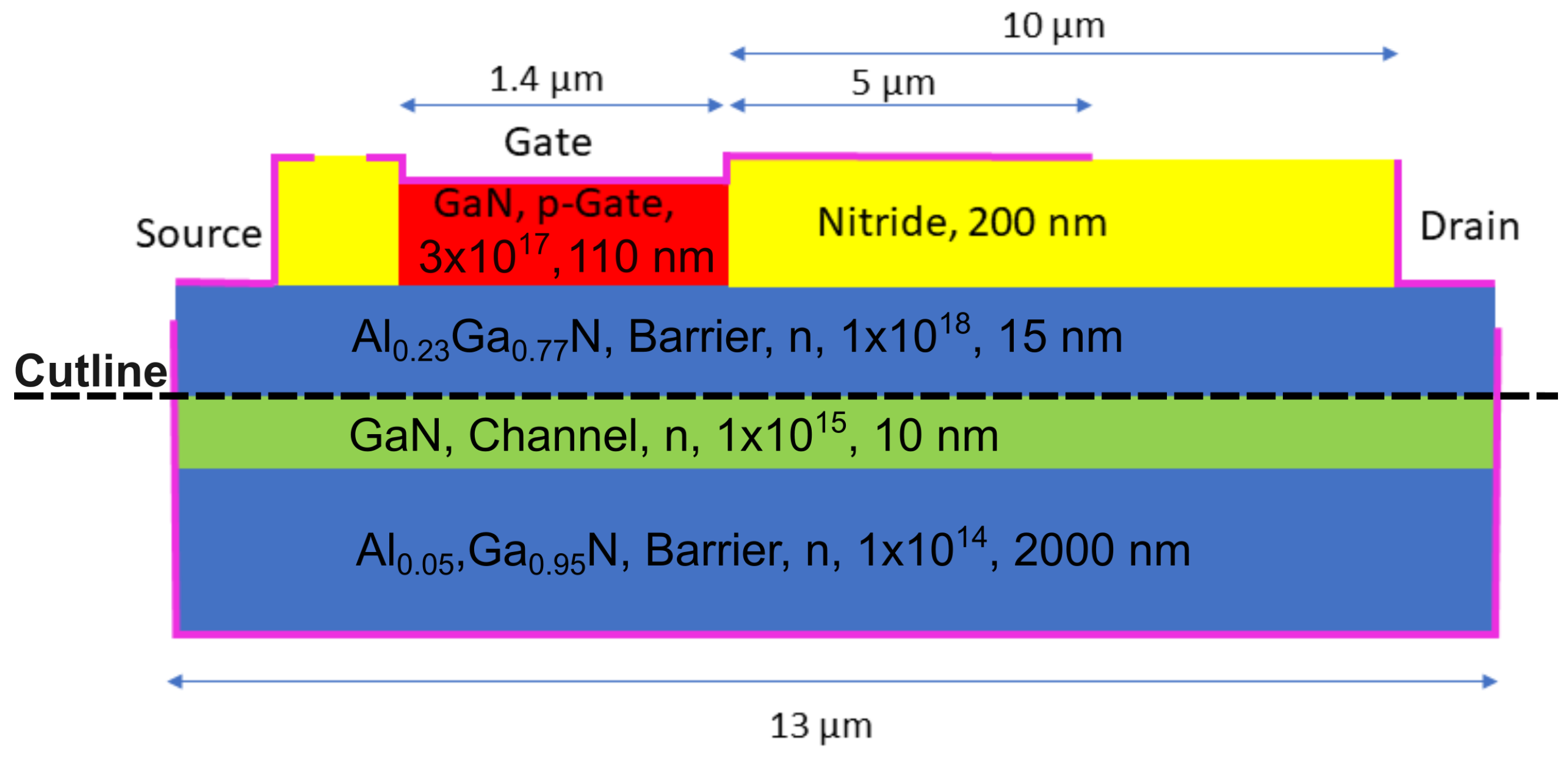
The starting point of our analysis involves the study of the thermal behavior of a GaN device under two different operating conditions: constant current switching (CCS) and short circuit (SC). For this purpose, the structure in Figure 1, which schematizes a normally-off AlGaN/GaN HEMT cell with a p-type gate and AlGaN Buffer, was simulated with the Synopsys TCAD tool [18].

Figure 1.
Two-dimensional structure of the GaN HEMT simulated in TCAD.
The structure is based on the one described in [19] and is formed by an buffer layer, a 10 nm GaN channel layer, and a 15 nm barrier layer. The gate is a 110 nm p-type GaN layer doped with Manganese; its length is 1.4 m, and field plate of 5 m is present. A single field plate was used to simplify the simulation even if in practice more field plates are used. This simplification has a very low impact on the results of our analysis, which is more concentrated on the current density that mainly influences the thermal behavior of the device.
The source and drain contacts are defined as Schottky with a metal work function of 4.3 eV, and the gate contact has been realized using the Schottky contact resistance model with the TCAD default values. The entire structure is 13 m long, and an area factor of about has been set to obtain an area of about 2.6 . The buffer contact was defined as both an electrical and a thermal node with a starting temperature of 300 K and by setting a thermal boundary condition with 0.0004 thermal resistance. These parameters were chosen according to [20] in order to simulate a device as similar as possible to a commercial 650-V/4-A GaN HEMT.
The presence of the traps in AlGaN and GaN was considered by introducing traps of donor type at the AlGaN/Nitride interface ( at 0.6 eV from MidGap) and of acceptor type at AlGaN/GaN ( at 0.23 eV from the conduction band), and in the buffer layer ( at 0.45 eV from the conduction band) [19]. The levels and concentrations were chosen to match the subtreshold slope of the – curve and the off-state leakage current.
The following physical models were used: Shockley–Read–Hall recombination, the Masetti mobility model, the Caughey–Thomas model to describe the high-field saturation effects, Fermi–Dirac statistics, and nonlocal band-to-band tunneling.
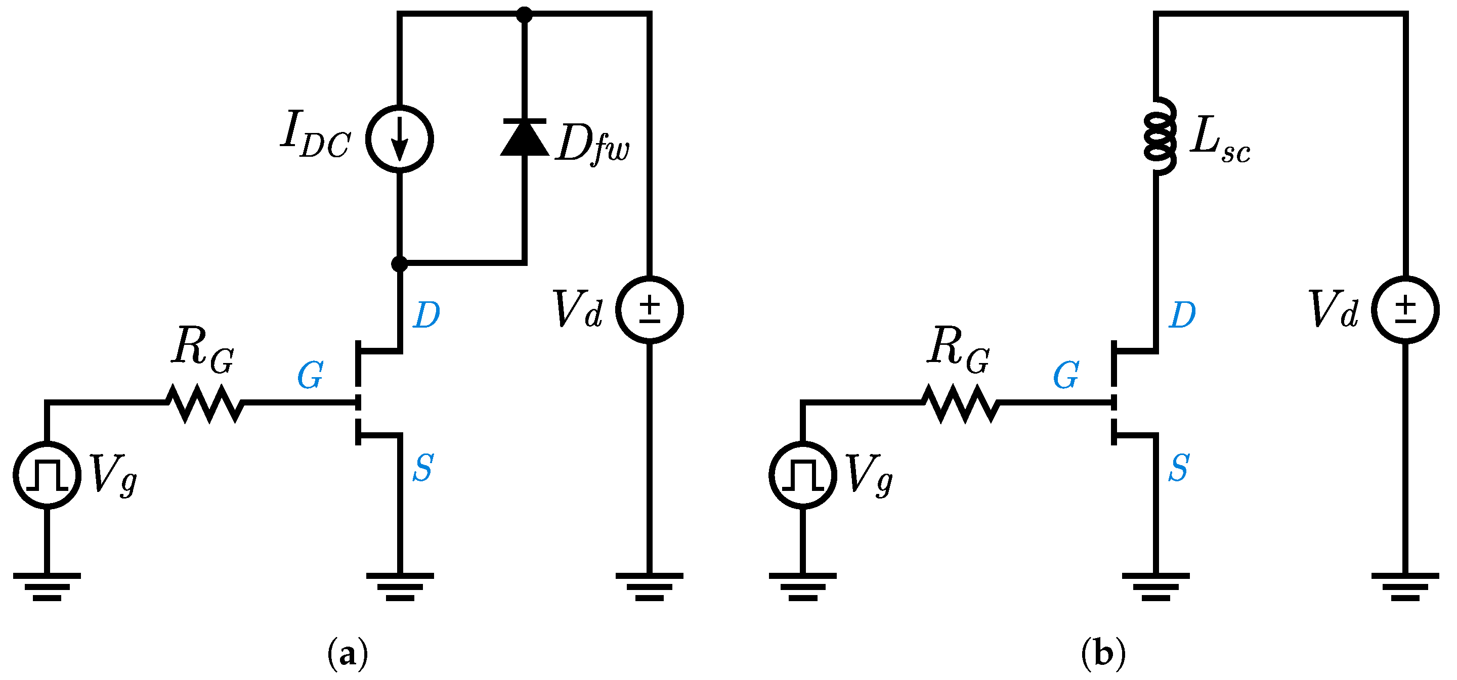
After carrying out static simulations to verify the structure’s breakdown voltage and DC characteristics, the TCAD mixed-mode tool was used to study the behavior of the device inserted into the circuits of Figure 2. The circuits were driven in both cases by connecting a voltage source to the gate through a 10 resistor . Figure 2a shows the circuit used for CCS, where a constant current source and an ideal freewheeling diode are placed at the drain of the device and the voltage source is used to set the drain voltage to 50 V. The hypothesis of using a constant current switching instead of inductive load switching does not affect the considerations on the thermal behavior carried out in the next sections, that is the object of this research. The SC was simulated by realizing the scheme of Figure 2b, where is a 10 nH inductor placed at the drain contact to simulate the parasitic inductance on the DC-link. The low value of guarantees that the device operates with low electrothermal budget, avoiding any critical condition.
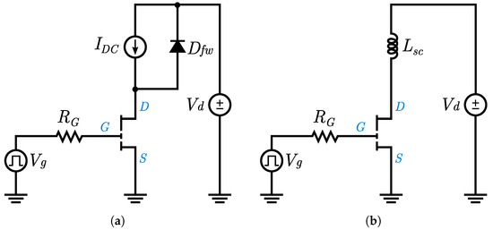
Figure 2.
Scheme of simulated circuits for CCS (a) and SC (b).
2.1. Constant Current Switching
The constant current switching was simulated applying a pulsed with a period of 2 s, 50% duty-cycle and 5 V amplitude. The current source supplies 4 A. Figure 3 shows the waveforms at the device terminals during a single period. The gate voltage (in green) and the drain voltage (divided by 5, in blue) refer to the left axis, while the current waveform (in red) refers to the right.
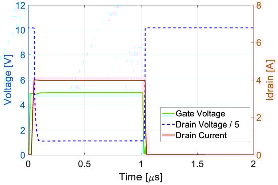
Figure 3.
TCAD simulations of the electrical waveforms in CCS during a single switching period.
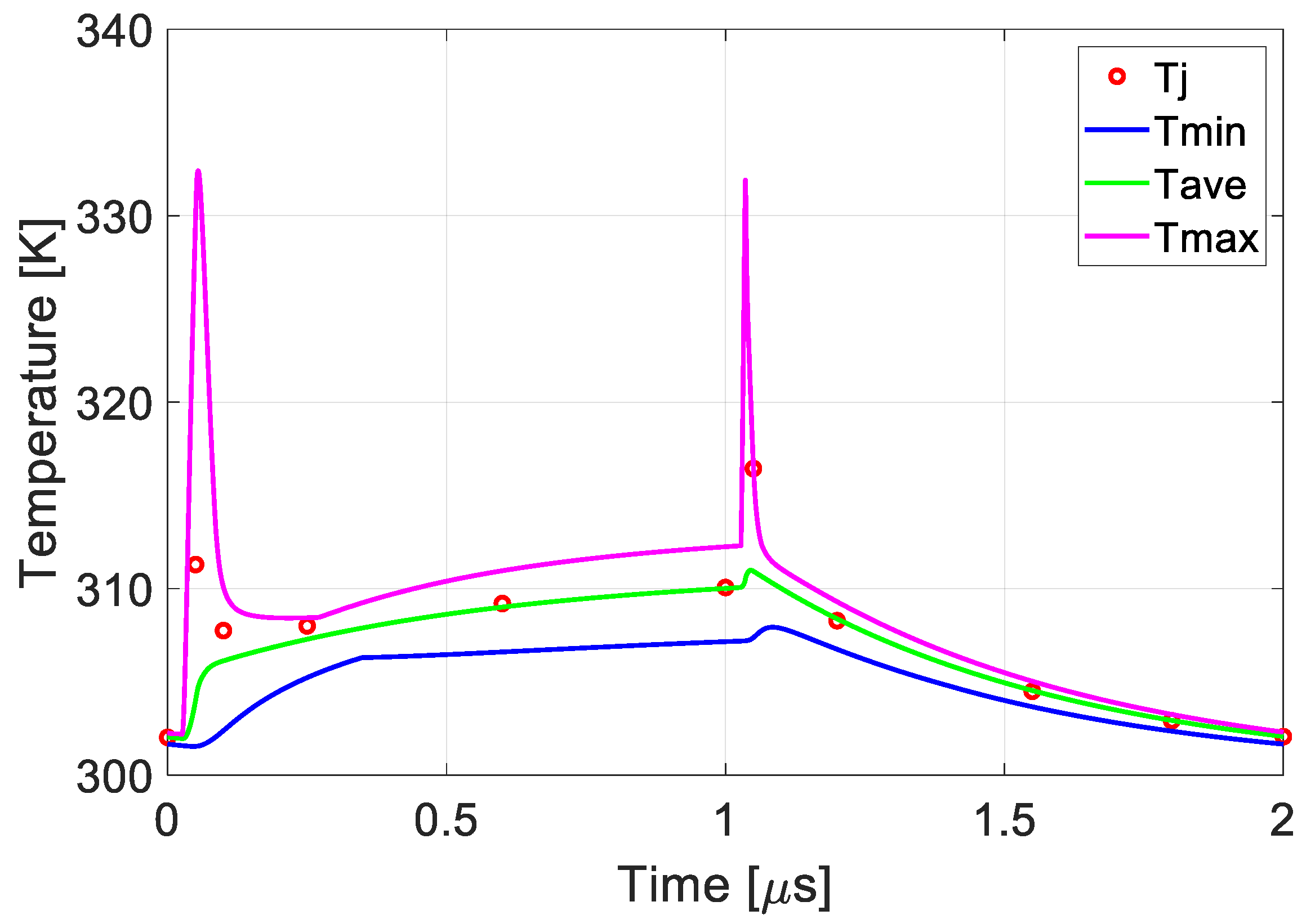
The instantaneous power dissipation, not reported in the figure, is maximum at the turn-on and turn-off switching transients (200 W at 0.046 s and 195 W at 1.03 s, respectively), while it is lower during the conduction (about 30 W). This power translates into heat produced inside the device, whose temperature will increase. The simulator, in addition to the electrical characteristics, provides the time dependence of minimum, average and maximum temperatures inside the device, identified as , and , respectively, and their graphs are shown in Figure 4. (magenta curve) has two peaks corresponding to the maximum power dissipation during the switching, showing an increase of about 30 K at these time instants with respect the initial temperature. However, this increase is located in a small volume of the device, as the average temperature calculated in the entire structure (green curve) remains between 300 and 311 K. The latter value is reached after about 1 s, when also reaches its highest value of 308 K (blue curve). The device returns to the initial thermal conditions after 2 s.
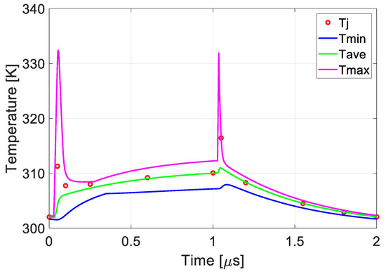
Figure 4.
Graph of temperatures (, , ) inside the device provided by TCAD during CCS. The red circles indicate the computed values of .
The curves in Figure 5 obtained automatically by TCAD do not provide important information like the location of possible critical points. A more detailed analysis of TCAD results is therefore necessary. For this purpose, the 2D spatial temperature distribution provided by TCAD was analyzed starting from the time-domain electrical waveforms of Figure 3. In particular, the one-dimensional temperature distribution was extracted from the 2D distributions along a cut line at the GaN/AlGaN interface where the 2DEG is formed. The obtained one-dimensional temperature profiles are plotted in Figure 5 for the time instants: 0 , 0.05 , 0.06 , 1.05 , 1.6 , 2 . At t = 0 , the temperature is fixed at 302 K and is uniform in the channel (blue curve). An increase is observed immediately after the device turn-on (t = 0.05 , green curve), with two peaks at the gate’s right edge and the field plate’s termination. Subsequently, the dissipated power decreases due to the reduction of the drain voltage with consequent temperature reduction (t = 0.06 , purple curve). This condition persists up to t = 1.05 in correspondence with the device turn-off transient, where the temperature increases (red curve), showing a peak under the gate region. After that, the device starts cooling down (yellow curve) and returns to the initial temperature after 2 (light blue curve). For completeness, the inset of Figure 5 reports the 2D lattice temperature distribution in the device at t = 0.05 , showing the two hottest regions at the gate’s right edge and the field plate’s termination. The TCAD simulation results were also used to extract , whose definition requires some attention. In fact, considering the strong variability of the temperature in the structure of the device (see Figure 5), it is necessary to preliminarily say what is meant by junction temperature. It is generally accepted [21] that should be considered as the average temperature of the conduction channel. In fact, important parameters such as the on-resistance of the device, the transconductance and partly the threshold voltage depend on this temperature. We then used the TCAD results to extract the values according to the following procedure: The one-dimensional channel temperature distribution was again extracted from the 2D distributions along a cut line at the GaN/AlGaN interface. was calculated as the average value of this temperature distribution. The results of this post-simulation analysis are reported as red circles in Figure 4. It is seen that the extracted values of overlap reasonably well with the curve except during device commutation, where is approximately 6 K higher than . Therefore, we can say that during CCS is comparable to the average temperature predicted by 2D simulations inside the device.
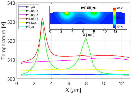
Figure 5.
Temperature profile at the GaN/AlGaN interface at different time instants during one switching period extracted from TCAD simulations. In the inset, the temperature distribution at t = 0.05 .
2.2. Short Circuit Operation
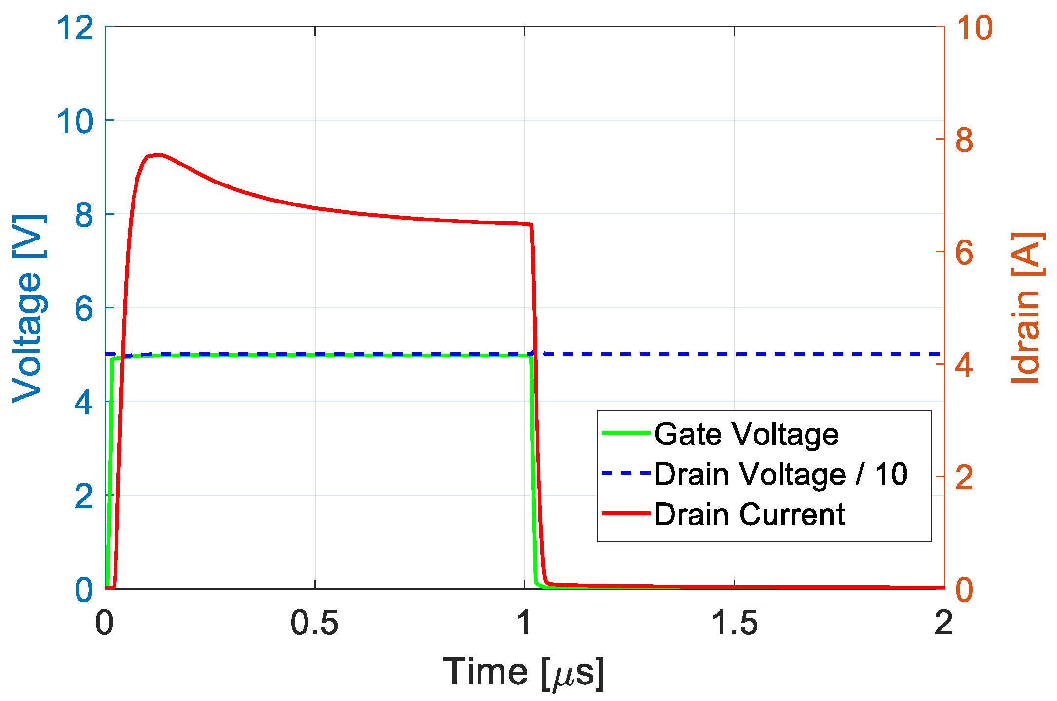
To simulate a type-I SC condition, described by the circuit of Figure 2b, a pulsed was used with 5 V amplitude and 1 duration, with the voltage fixed to 50 V. The simulated waveforms of the gate voltage (in green), the drain voltage (divided by 10, in blue) and the drain current (in red) are reported in Figure 6. The SC current reaches a peak value of about 8 A and then decreases to 6.4 A, returning to zero when the device is turned off. The instantaneous power dissipation, not reported, has a peak value of 400 W, while its mean value during the gate pulse duration is about 350 W, leading to the increase in temperature, which causes the SC current reduction and the progressive heating of the device.
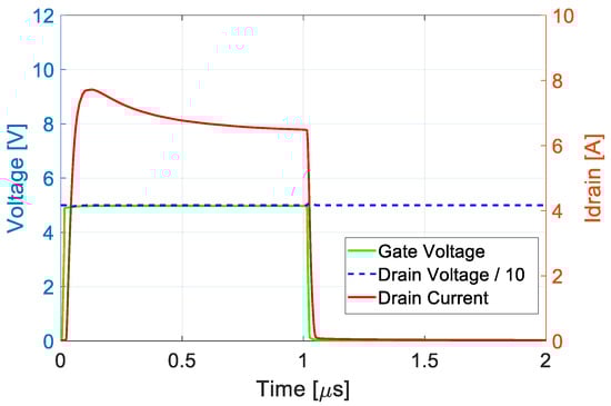
Figure 6.
TCAD simulation of the electrical waveforms during the SC.
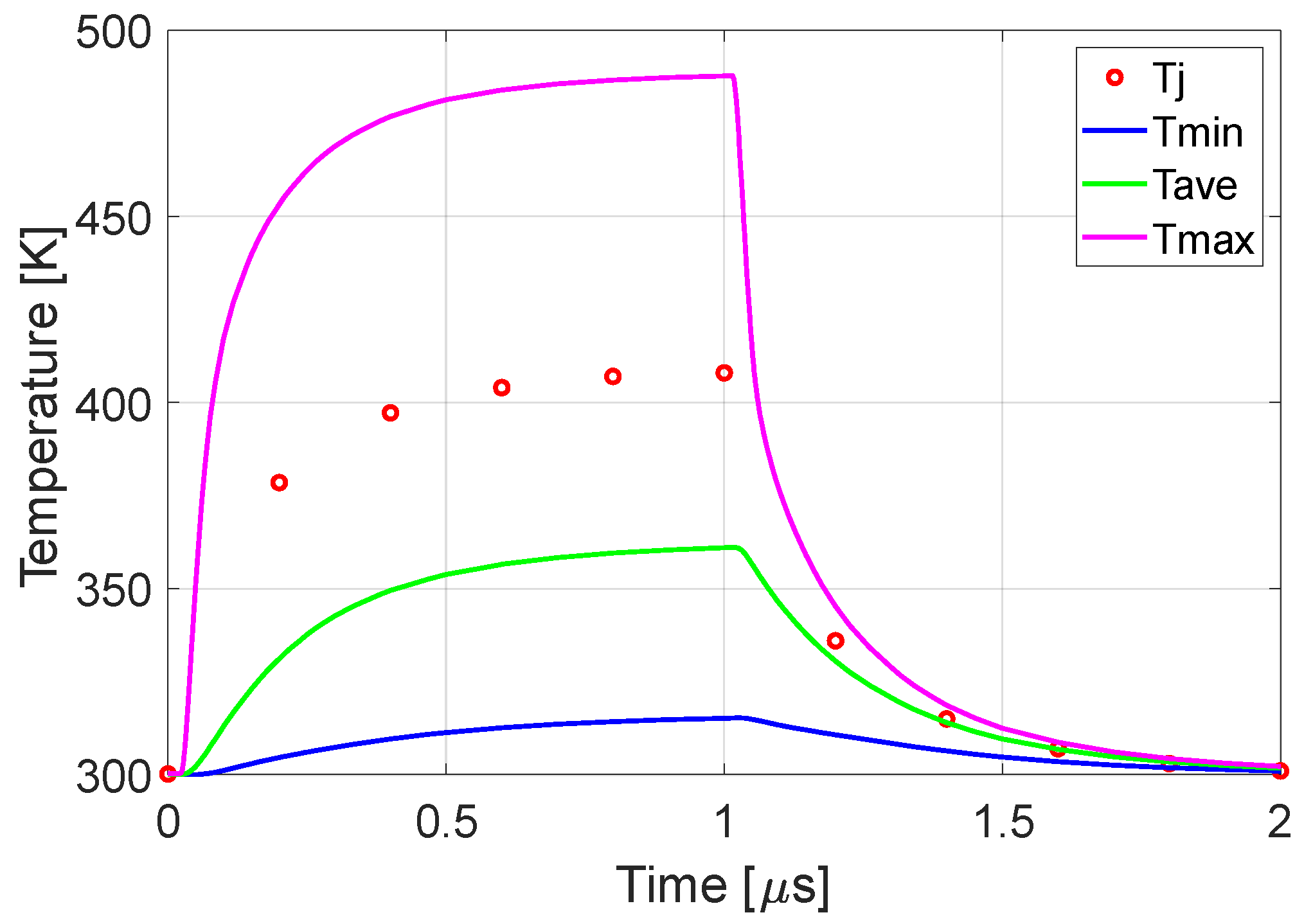
Figure 7 reports the time evolution of , , and during the SC, while the red circles represent the temperature extracted with the same procedure described before. These curves appear very different from those in Figure 4. As the involved power is more significant, the temperature is higher in the whole device. The maximum temperature (480 K) is reached inside the device at t = 1 and is about 80 K higher than the extracted , which in turn is 50 K higher than the maximum value of . It follows that during the SC, the definition of itself is not consistent as the temperature is strongly not homogeneous along the channel. In fact, the temperature distribution along the GaN/AlGaN interface during the SC, reported in Figure 8, shows that a hot spot is located at the right edge of the gate (x = 2.88 m), where the temperature reaches the maximum value of 480 K at t = 1 (red curve) before decreasing (yellow curve) and returning to the starting value after 2 (light blue curve). The inset of Figure 8 shows the 2D temperature distribution at t = 1 (the end of the SC), highlighting the presence of the hot spot.
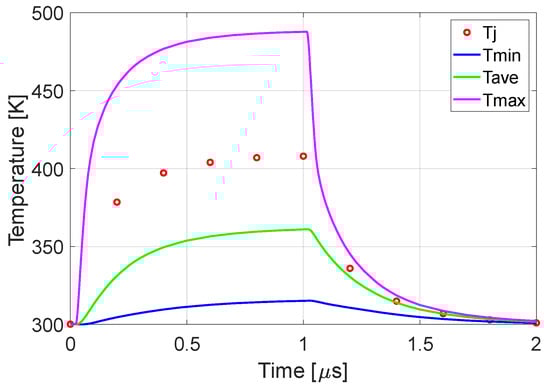
Figure 7.
Graph of temperatures (, , ) inside the device provided by TCAD during the SC. The red circles indicate the computed values of .
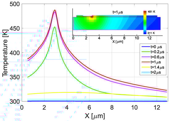
Figure 8.
Temperature profile at the GaN/AlGaN interface at different time instants during the SC. In the inset, the temperature distribution for t = 1 .
Figure 8 confirms that the definition of as the mean channel temperature is not appropriate during the SC operation of the GaN HEMT, because of the huge temperature gradient along the channel and the hot spot presence.
3. Limitations of LTSpice Model for Thermal Analysis during SC
The results of Figure 4 and Figure 7 highlight that the two analyzed operating conditions show completely different thermal responses. The consequence is that when using simulation tools such as LTSpice, they are not able to correctly simulate the channel temperature during the SC. In fact, GaN HEMTs’ thermal models used in SPICE-based tools are derived assuming uniform heat distribution along the channel [15,16]. This fact leads to the determination of an equivalent thermal impedance of the device that is valid only during the normal operation of the device, while it deviates from the real behavior when an abnormal operating condition is simulated, as in the case of the SC. As a consequence, although the simulation of a GaN HEMT during SC can be used to obtain an estimation of drain and gate currents [17,22], their temperature dependence is affected by the inaccuracy and the unreliability of the thermal model.
To demonstrate the previous consideration, we compared the TCAD and the LTSpice simulations of a commercial 650-V/4-A GaN HEMT. We used the manufacturer’s LTSpice Level 3 model, which includes the Cauer thermal model, to reproduce the device behavior in the same operating conditions as in the previous section: = 5 V, = 50 V.
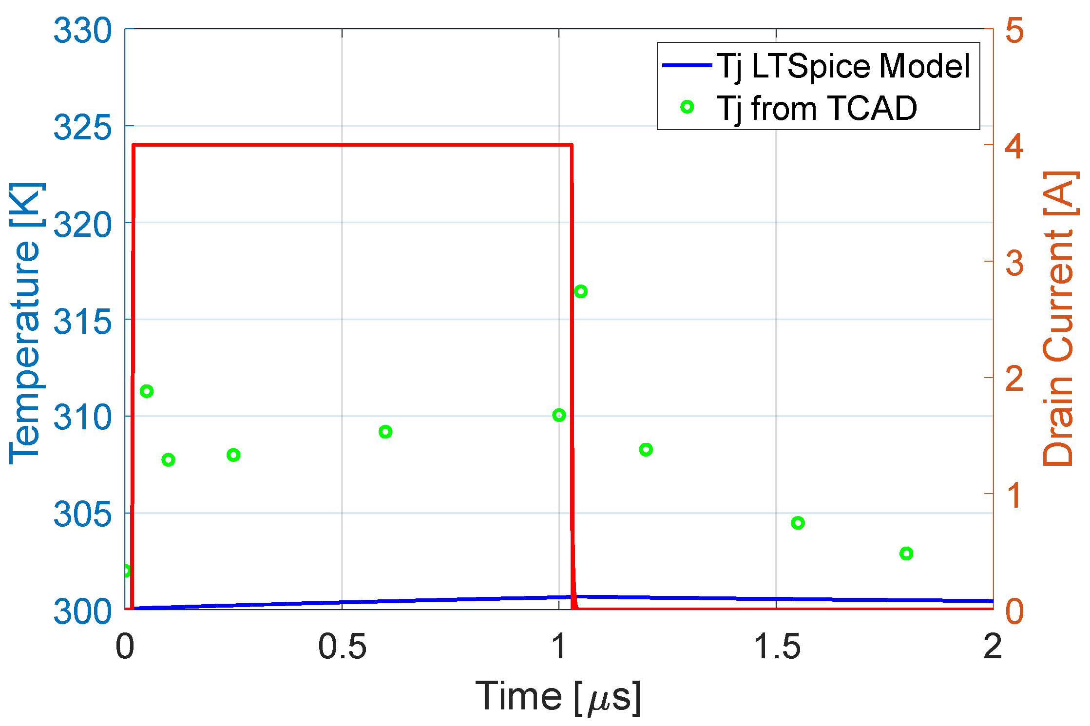
The LTSpice simulation results of CCS are reported in Figure 9, which shows the drain current (in red) and (in blue). simulated in LTSpice differs from that of TCAD (green circles), also reported in Figure 9, for less than 10 K if we exclude the points related to the maximum dissipated power during the turn-on and turn-off transitions.
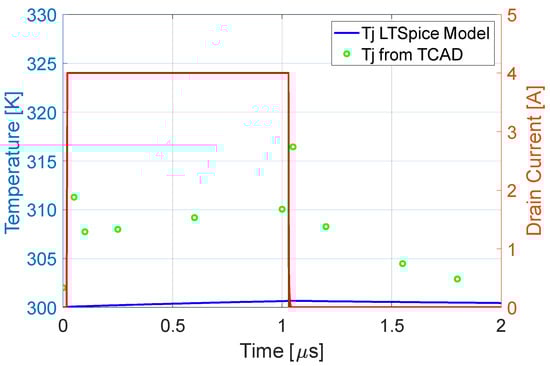
Figure 9.
Drain current (in red) and simulated with LTSpice during CCS at = 5 V and = 50 V. The green circles represent extracted from TCAD (see Section 2).
Figure 10 shows the simulated waveforms in SC conditions. In this case, a substantial difference in between LTSpice and TCAD simulations can be observed. At the end of the SC, from LTSpice simulation is about 330 K, while it is 410 K from TCAD, with a difference of about 80 K. This happens because LTSpice uses the same thermal model for both CCS and SC conditions, with the only difference in the dissipated power being the input of the thermal network. This fact leads to an error in evaluating the temperature during the SC event. It must be noted that in SC was computed according to the procedure described in Section 2 and does not represent the maximum temperature reached in the hot spot. In this case, the error of the LTSpice simulation would be even higher, equal to about 150 K (compare Figure 7 and Figure 10).
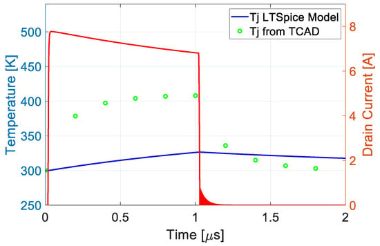
Figure 10.
Drain current (in red) and simulated with LTSpice during SC at = 5 V and = 50 V. The green circles represent extracted from TCAD (see Section 2).
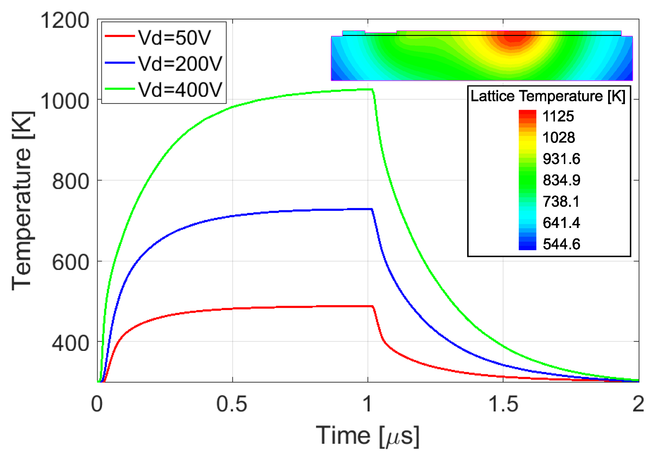
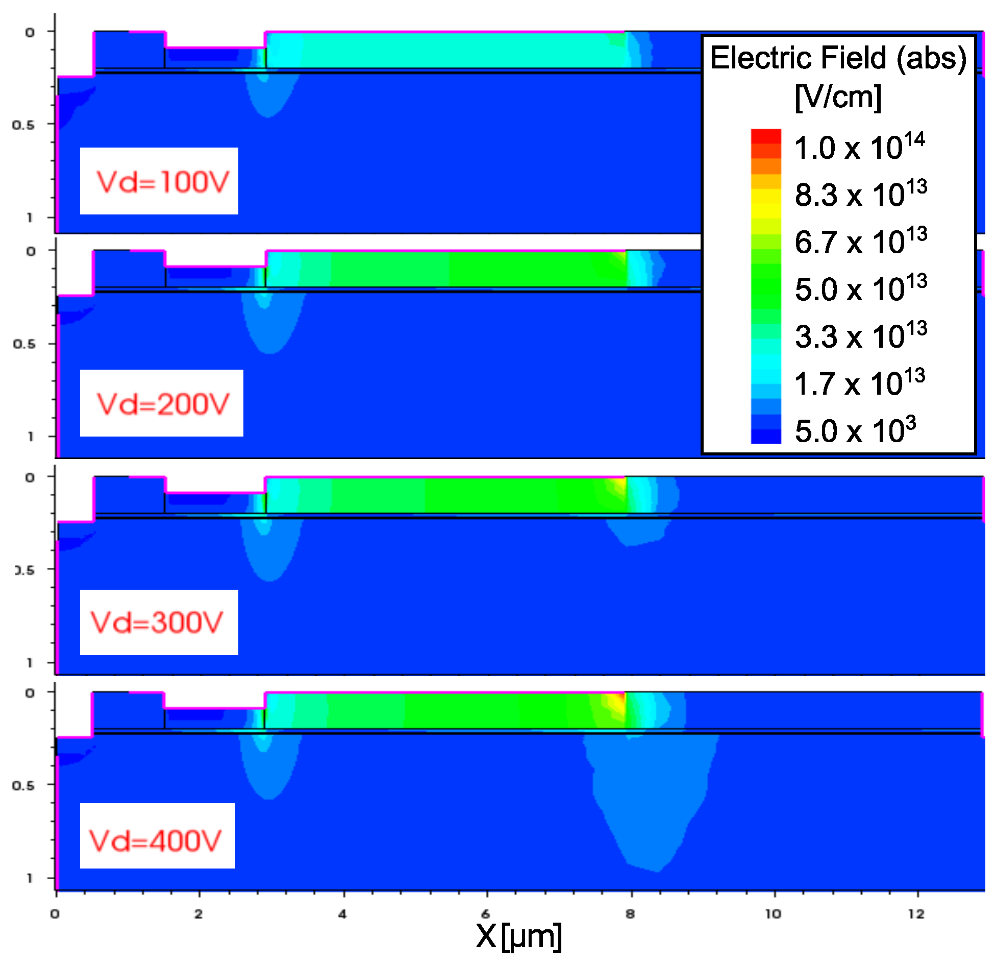
In fact, the SPICE model neglects the presence of a hot spot where the temperature () is much higher than the average temperature along the channel. The impact of the hot spot temperature could be potentially dangerous as the drain voltage increases. In fact, as shown in Figure 11, as increases from 50 V to 400 V, the hot spot temperature increases, exceeding 1000 K at = 400 V. The temperature range between 900 K and 1000 K is correlated with the device failure [23,24,25]. The inset of Figure 11 reports the temperature distribution at t = 1 for = 400 V and shows that the hot spot is located at the end of the field plate. As shown in Figure 12, where 2D distribution of the electric field modulus is reported for = 100 V, 200 V, 300 V and 400 V, as the drain voltage increases the effectiveness of the field plate reduces and the maximum of the electric field moves from the right edge of the gate to the field plate’s edge, which becomes the most critical point in the structure, as found in [6,13].
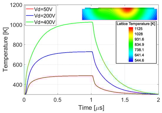
Figure 11.
Time evolution of during the SC at different drain voltages and = 5 V. The temperature distribution at t = 1 and = 400 V is also reported in the inset.

Figure 12.
Electric field inside the structure at fixed = 5 V for different values of .
The limitations of the LTSpice model to describe the SC behavior of the GaN HEMT could be expected if we consider the hypothesis used to derive the thermal model. The Cauer model describes each layer of the device through an electrical equivalent network, derived under the assumption of a homogeneous temperature in the channel [15], while TCAD simulations showed a strong spatial distribution of the temperature.
4. Experimental Measurements
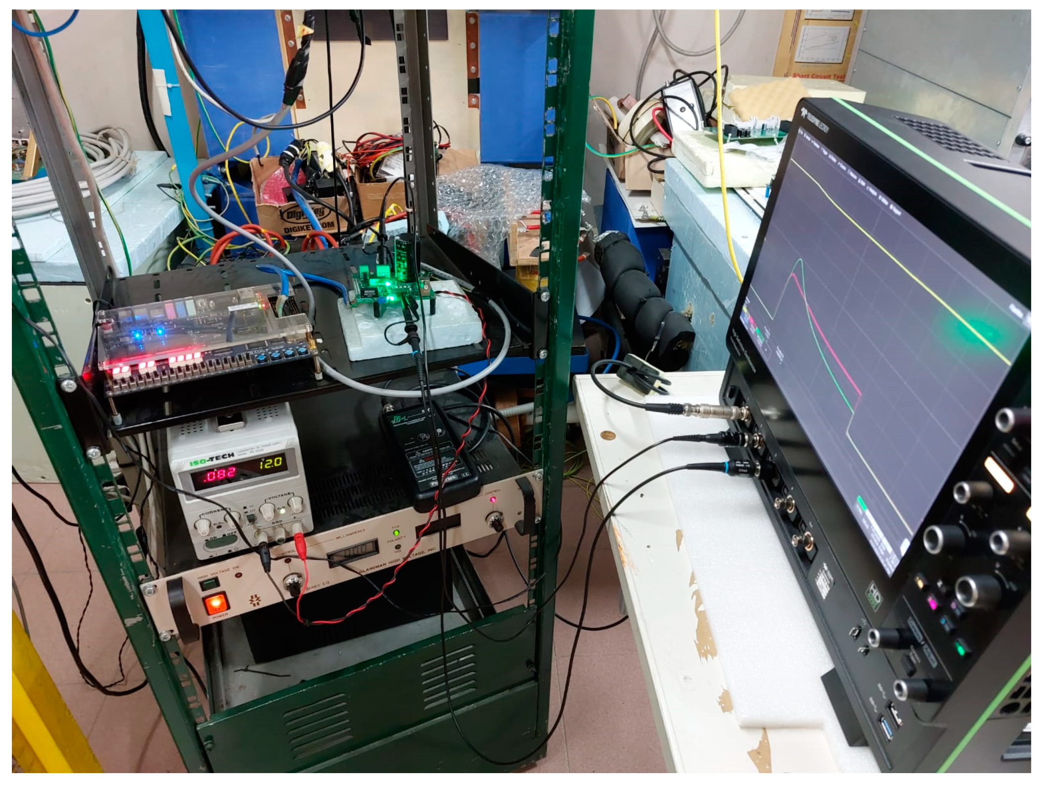
From the considerations of Section 3, we should expect that an inaccurate estimate of also affects the LTSpice simulated drain current. To explore this aspect, measurements under type-I SC conditions were carried out on two samples of a commercial 650 V/4 A GaN device [20]. A picture of the experimental setup is shown in Figure 13.
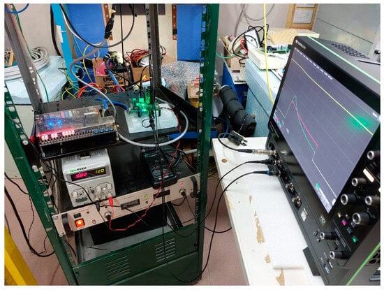
Figure 13.
Picture of the experimental setup.
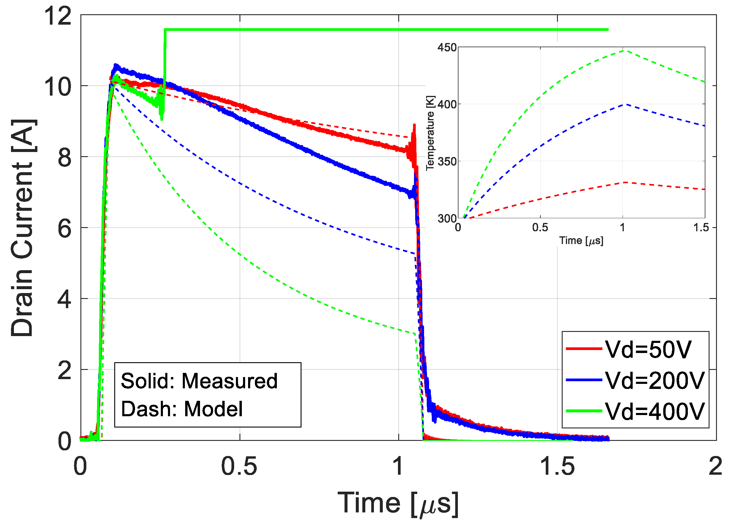
For the experimental tests, we used the same setup described in [13], whose picture is shown in Figure 13. The drain contact of the low-side device was directly short-circuited to the DC-link to replicate the test circuit of Figure 2b. The device was turned on for 1 by applying a voltage pulse on the gate with amplitude = 5 V through a 10 gate resistor. The drain voltage was varied using as DC-link voltage 50 V, 200 V, and 400 V. The drain current waveforms measured during the tests (solid lines) are reported in Figure 14, compared with those simulated with the Level 3 LTSpice model (dashed lines) with the case temperature set to 300 K.
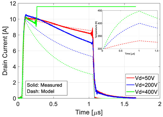
Figure 14.
Comparison between the current waveforms measured during the SC (solid lines) and those from LTSpice simulations (dashed lines) at different drain voltages. In the inset, the simulated are also reported.
The experimental waveforms show that at different the peak value of is quite constant, while the temperature increase is responsible of the reduction, which is more pronounced increasing the drain voltage. The failure of the device after 200 ns at = 400 V indicates that the temperature has reached a critical value. If we compare experimental waveforms with LTSpice simulations, we note that the current peak value is quite well estimated by the model, while significant differences are observed in the time evolution of the current. For low drain voltage ( = 50 V), the simulated current is slightly overestimated. Increasing , the reduction in the simulated current is more pronounced than the related experimental curve. In particular, if we consider the case = 400 V, the strong reduction in seems to indicate a huge increase in the device’s . This statement is not confirmed by the junction temperature evaluated by the LTSpice model. From the values reported in the inset of Figure 14 we can note that remains below 450 K even at 400 V, while the observed experimental failure of the device suggests an internal temperature much higher.
5. Proposed Model
A comprehensive model for the simulation of the GaN HEMT during SC should provide a correct estimation, necessary to obtain a realistic dependence from the temperature, and an estimation of the hot spot temperature reached inside the device, that affects its robustness.
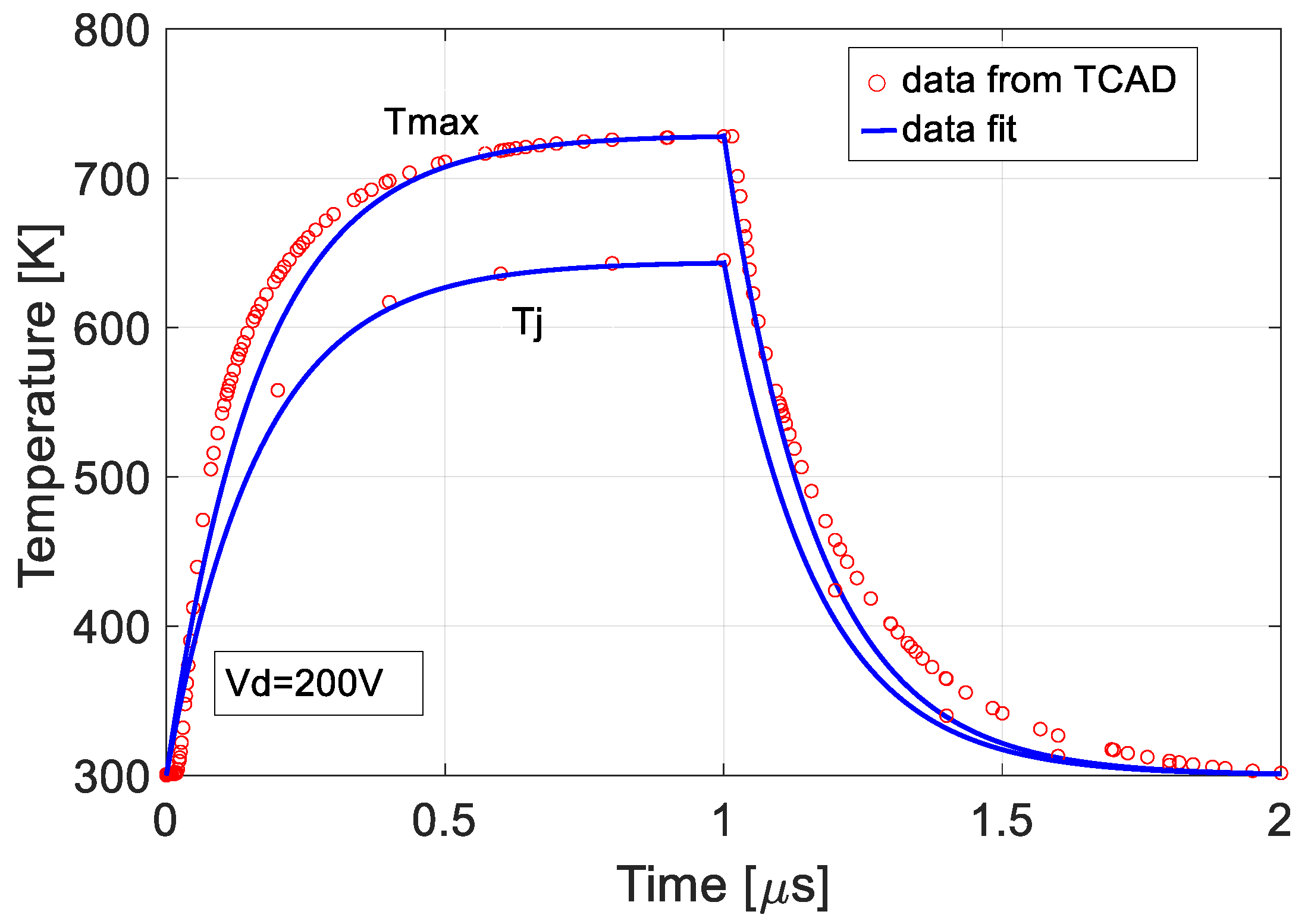
Based on the results of TCAD simulations in this section we propose a simple thermal model that reproduces the real temperature dependence of and provides the hot spot temperature () inside the device. Due to the fast dynamic of the SC event, the device can be considered an adiabatic system where the heat transfer is strongly constrained in the first layers of the structure, not involving the case and the environment [26]. This consideration allows us to derive a simple thermal model with a single time constant. In fact, under this assumption, and curves can be fitted with adequate accuracy for all drain voltages, as reported, for example, in Figure 15 for = 200 V.
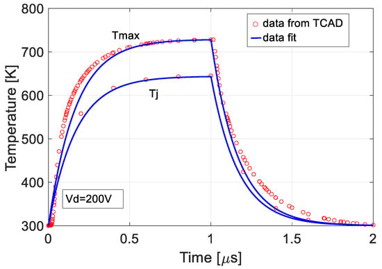
Figure 15.
Fitting of and using a single-time constant model.
The fitting functions are expressed by (1) and (2) during the SC pulse and during the cooling phase, respectively.
and are fitting parameters that represent the equivalent thermal resistance and capacitance and they are a function of the applied drain voltage . is the mean power dissipated during the SC pulse and is computed from TCAD simulations. represents the case temperature and is the temperature at the onset of the turn-off after the SC phase, that is = 1 in this case.
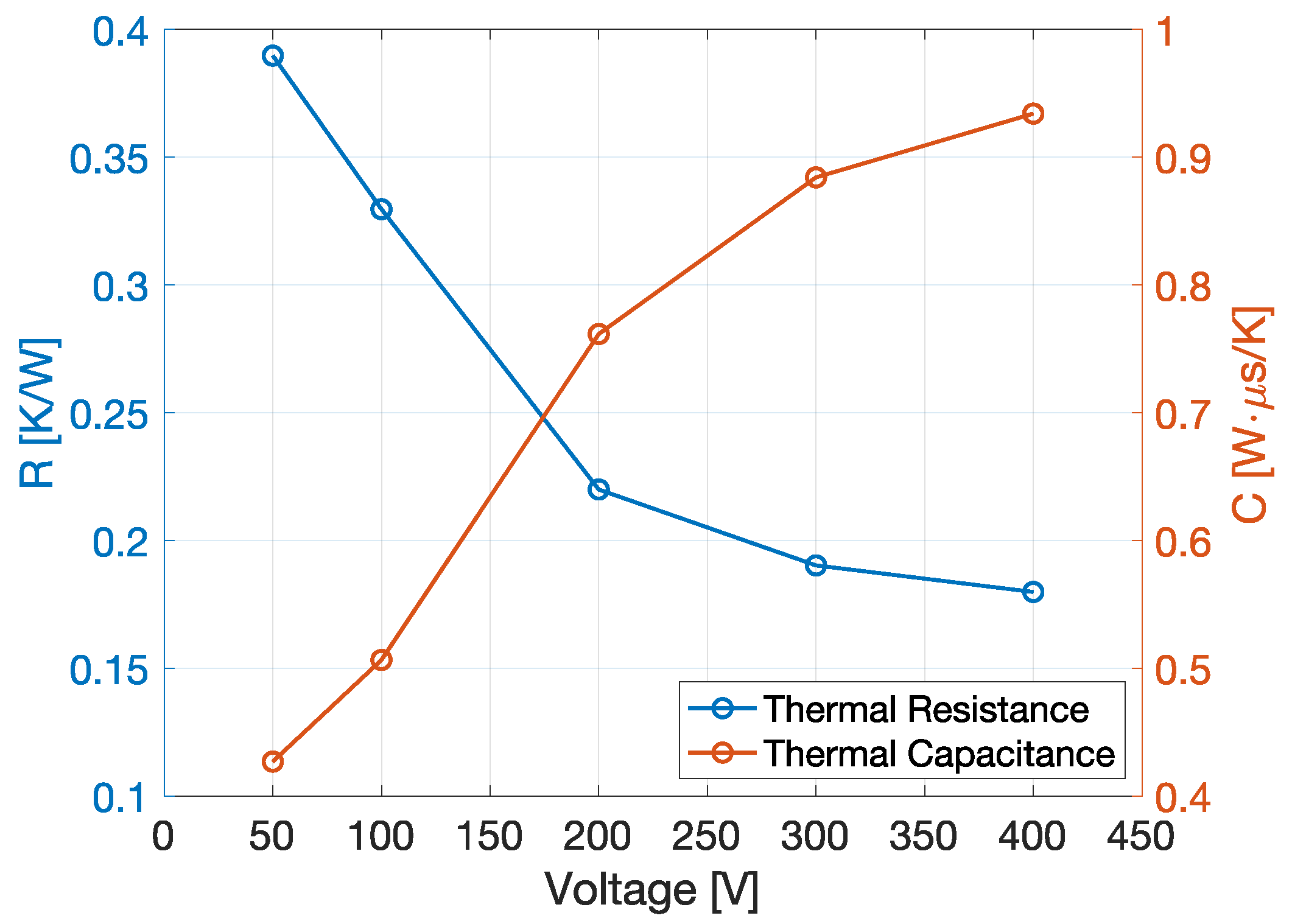
The fitting procedure was initially applied to curves varying from 50 V to 400 V. The extracted values of and are shown in Figure 16 at different . It is worth noting that the thermal time constant remains equal to 167 ns for all voltages.

Figure 16.
Thermal parameters extracted from fitting of as a function of .
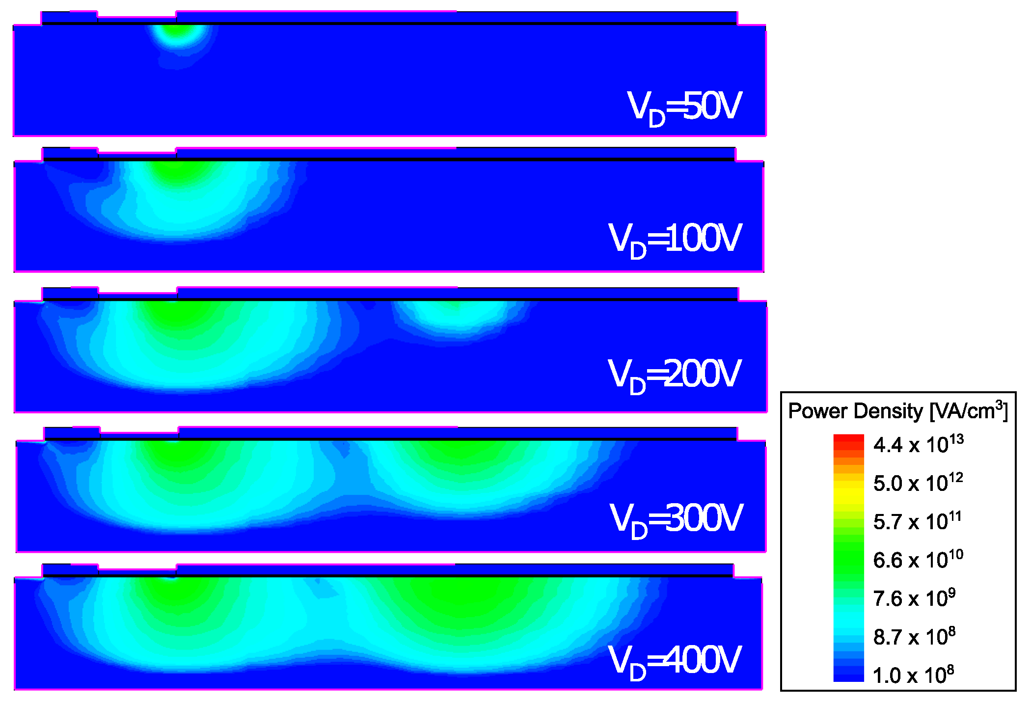
In the manufacturer’s thermal model for CCS, it is possible to relate and to the geometrical and physical parameters of the device, because both the power density distribution and junction temperature are supposed to be uniform along the whole channel. Figure 17 shows that during the SC, the power density has a different space distribution depending on the applied , leading to the dependence of and on this parameter. In particular, becomes larger for higher values, as it is proportional to the volume involved in the heat transfer, which increases with , as depicted in Figure 17. On the other hand, for increasing , the power density distribution involves a larger surface, reducing the effective length between the heat generation and the substrate, leading to lower values of .
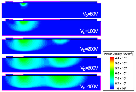
Figure 17.
Simulated power density distribution inside the structure for different .
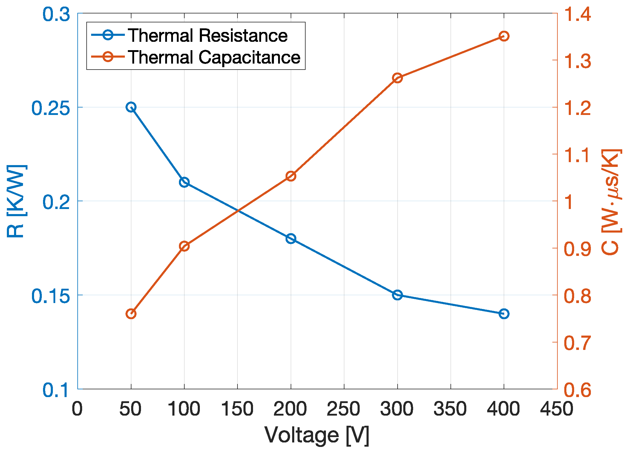
The same procedure was used to estimate and that fit , whose values are reported in Figure 18. In this case, the value of is found to be 189 ns for all voltages.
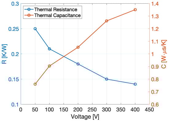
Figure 18.
Thermal parameters extracted from fitting of as a function of .
The two networks shown in Figure 19 represent the electrical equivalent circuit described by (1) and (2), which can be used to estimate both and during the SC. They have been inserted in the LTSpice model of the GaN device, substituting the manufacturer thermal model. It is worth noting that the electrical parasitic capacitances and resistances were already included in the manufacturer model and they have not been modified. A further thermal pin was added to the subcircuit of the GaN HEMT for the sense of , as shown in Figure 19.
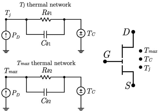
Figure 19.
Schematic of the thermal networks and the modified symbol for the GaN HEMT used for the LTSpice simulations.
The thermal networks receive as input the instantaneous power dissipation given by , where is a function of , , and defined by (3), as described in [20,27].
The dependence with , expressed in degrees Celsius, is taken into account through (4), where is a parameter related to the output and transfer characteristics and is a fitting parameter taking into account the temperature characteristic.
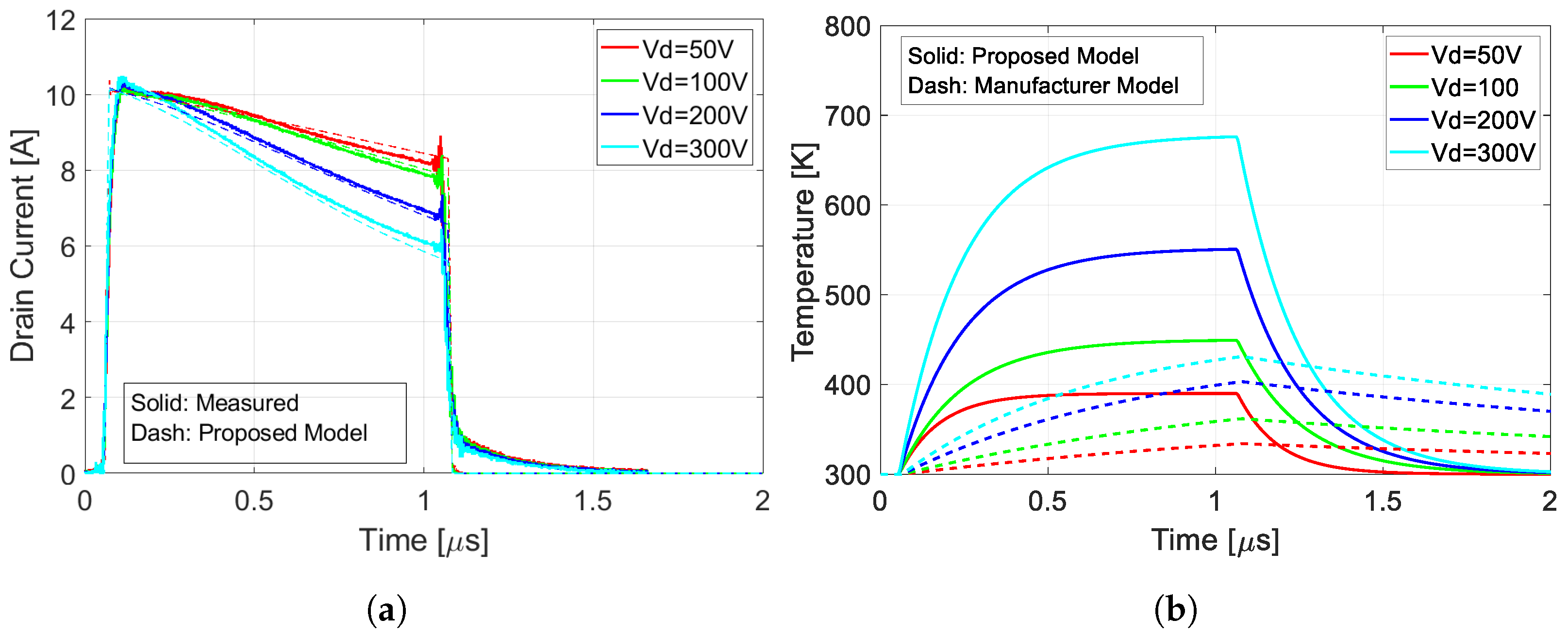
As a first result of the application of the proposed model, we simulated and during the SC for different . In Figure 20a, the simulated waveforms are compared with the experimental ones, showing a valuable improvement of accuracy with respect to the manufacturer model (compared with Figure 14). In Figure 20b, we reported the simulated obtained with the proposed model in comparison with the manufacturer model.
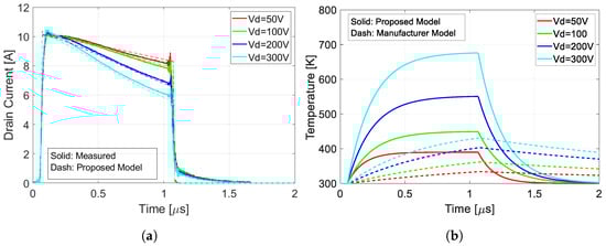
Figure 20.
(a) Comparison of measured with proposed model; (b) comparison between simulated using manufacturer’s and proposed model.
Although simulated with the manufacturer model is much lower compared to the proposed model, its influence on is overestimated, as already highlighted in Figure 14. This observation implies the need to modify the thermal dependence of in (4) by changing the coefficient from 0.0044 to 0.0013 °C−1, while remains equal to 0.99 A.
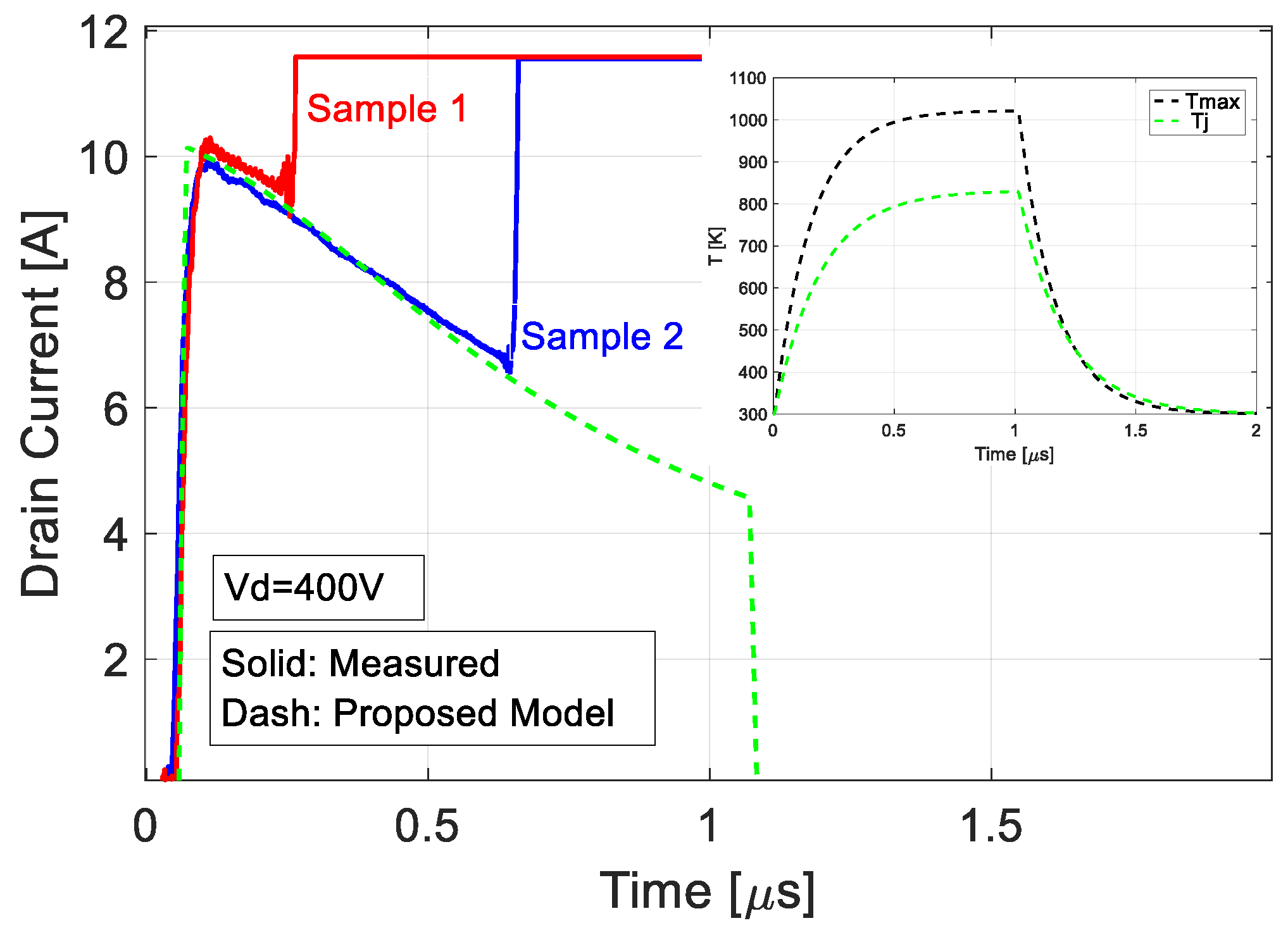
Finally, the proposed model provides an estimation of the maximum temperature reached inside the device and gives information about its possible failure. Experimental measurements performed on two samples of the tested device show that the GaN HEMT fails after few hundreds of nanoseconds at = 400 V, as reported in Figure 21. For this voltage value, as highlighted in the inset the estimated becomes higher than the failure limit of 900 K measured for the GaN/AlGaN structures [23,25].
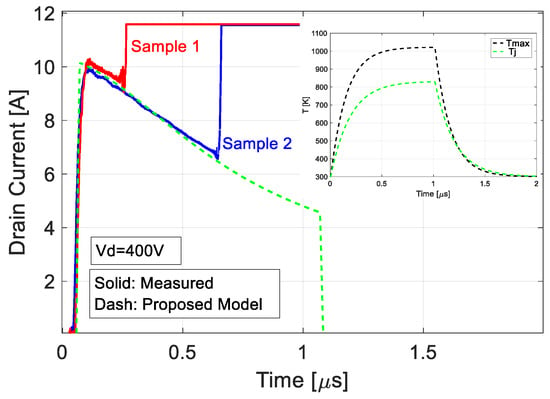
Figure 21.
Measured and simulated at = 400 V for two samples. The simulated and are plotted in the inset.
6. Conclusions
The GaN HEMT model commonly used in circuit simulators cannot accurately predict the behavior of the device during abnormal operations such as SC. A correct estimation of the junction temperature is necessary to accurately simulate the drain current during the SC, but it is not sufficient to give information about the possible failure of the device, which instead is related to the maximum temperature reached inside the device. Based on TCAD simulations and experimental measurements, we derived two thermal networks to estimate both junction and maximum temperature, which can be included in the device LTSpice model. The proposed model reproduces with good accuracy the experimentally measured drain current of 650 V/4 A GaN HEMTs and the estimated justifies the experimentally observed failures.
Author Contributions
Conceptualization, S.P., A.S. and G.B.; methodology, S.P., A.S. and G.B.; software, A.S., G.C.P. and F.V.; validation, S.P. and A.S.; formal analysis, S.P., A.S., F.V. and G.B.; investigation, A.S., G.C.P. and E.M.; resources, S.P., A.S., G.C.P. and E.M.; data curation, A.S. and S.P.; writing—original draft preparation, A.S., S.P. and G.B.; writing—review and editing, S.P., A.S., G.C.P., E.M., F.V. and G.B.; visualization, S.P. and A.S.; supervision, G.B.; project administration, A.S. and G.B.; funding acquisition, A.S. and G.B. All authors have read and agreed to the published version of the manuscript.
Funding
This research was funded by the Ministry of University and Research under the auspices of Research Projects of National Relevance n:2017 WA5ZT3 CUP N.H33C22000420001 and by Project Ecosistema dell’innovazione—Rome Technopole financed by EU in NextGenerationEU plan through MUR Decree n.1051 23.06.2023—CUP H33C22000420001.
Data Availability Statement
The raw data supporting the conclusions of this article will be made available by the authors on request.
Conflicts of Interest
The authors declare no conflicts of interest.
References
- Millán, J.; Godignon, P.; Perpiñà, X.; Pérez-Tomás, A.; Rebollo, J. A Survey of Wide Bandgap Power Semiconductor Devices. IEEE Trans. Power Electron. 2014, 29, 2155–2163. [Google Scholar] [CrossRef]
- Chen, K.J.; Häberlen, O.; Lidow, A.; Tsai, C.l.; Ueda, T.; Uemoto, Y.; Wu, Y. GaN-on-Si Power Technology: Devices and Applications. IEEE Trans. Electron Devices 2017, 64, 779–795. [Google Scholar] [CrossRef]
- Sun, J.; Wei, J.; Zheng, Z.; Lyu, G.; Chen, K.J. Distinct Short Circuit Capability of 650-V p-GaN Gate HEMTs under Single and Repetitive Tests. In Proceedings of the 2020 32nd International Symposium on Power Semiconductor Devices and ICs (ISPSD), Vienna, Austria, 13–18 September 2020; pp. 313–316. [Google Scholar] [CrossRef]
- Sun, J.; Zhong, K.; Zheng, Z.; Lyu, G.; Chen, K.J. Short-Circuit Failure Mechanisms of 650-V GaN/SiC Cascode Devices in Comparison With SiC MOSFETs. IEEE Trans. Ind. Electron. 2022, 69, 7340–7348. [Google Scholar] [CrossRef]
- Landel, M.; Gautier, C.; Labrousse, D.; Lefebvre, S. Experimental study of the short-circuit robustness of 600V E-mode GaN transistors. Microelectron. Reliab. 2016, 64, 560–565. [Google Scholar] [CrossRef]
- Riccio, M.; Romano, G.; Maresca, L.; Breglio, G.; Irace, A.; Longobardi, G. Short circuit robustness analysis of new generation Enhancement-mode p-GaN power HEMTs. In Proceedings of the 2018 IEEE 30th International Symposium on Power Semiconductor Devices and ICs (ISPSD), Chicago, IL, USA, 13–17 May 2018; pp. 104–107. [Google Scholar] [CrossRef]
- Li, H.; Li, X.; Wang, X.; Lyu, X.; Cai, H.; Alsmadi, Y.M.; Liu, L.; Bala, S.; Wang, J. Robustness of 650-V Enhancement-Mode GaN HEMTs Under Various Short-Circuit Conditions. IEEE Trans. Ind. Appl. 2019, 55, 1807–1816. [Google Scholar] [CrossRef]
- Riccio, M.; Romano, G.; Borghese, A.; Maresca, L.; Breglio, G.; Irace, A.; Longobardi, G. Experimental analysis of electro-thermal interaction in normally-off pGaN HEMT devices. In Proceedings of the 2018 IEEE International Conference on Electrical Systems for Aircraft, Railway, Ship Propulsion and Road Vehicles & International Transportation Electrification Conference (ESARS-ITEC), Nottingham, UK, 7–9 November 2018; pp. 1–6. [Google Scholar] [CrossRef]
- Fernández, M.; Perpiñà, X.; Roig-Guitart, J.; Vellvehi, M.; Bauwens, F.; Tack, M.; Jordà, X. Short-Circuit Study in Medium-Voltage GaN Cascodes, p-GaN HEMTs, and GaN MISHEMTs. IEEE Trans. Ind. Electron. 2017, 64, 9012–9022. [Google Scholar] [CrossRef]
- Xue, P.; Maresca, L.; Riccio, M.; Breglio, G.; Irace, A. A Comprehensive Investigation on Short-Circuit Oscillation of p-GaN HEMTs. IEEE Trans. Electron Devices 2020, 67, 4849–4857. [Google Scholar] [CrossRef]
- Abbate, C.; Busatto, G.; Sanseverino, A.; Tedesco, D.; Velardi, F. Experimental study of the instabilities observed in 650V enhancement-mode GaN HEMT during short circuit. Microelectron. Reliab. 2017, 76, 314–320. [Google Scholar] [CrossRef]
- Abbate, C.; Busatto, G.; Sanseverino, A.; Tedesco, D.; Velardi, F. Failure mechanisms of enhancement mode GaN power HEMTs operated in short circuit. Microelectron. Reliab. 2019, 100, 113454. [Google Scholar] [CrossRef]
- Abbate, C.; Busatto, G.; Sanseverino, A.; Tedesco, D.; Velardi, F. Failure analysis of 650 V enhancement mode GaN HEMT after short circuit tests. Microelectron. Reliab. 2018, 88, 677–683. [Google Scholar] [CrossRef]
- Fernández, M.; Perpiñà, X.; Roig, J.; Vellvehi, M.; Bauwens, F.; Jordà, X.; Tack, M. P-GaN HEMTs Drain and Gate Current Analysis Under Short-Circuit. IEEE Electron Device Lett. 2017, 38, 505–508. [Google Scholar] [CrossRef]
- GaN Systems Inc. Modeling the Thermal Behavior of GaNPx® and PDFN Packages Using RC Thermal Spice Models; GaN Systems Inc.: Stittsville, ON, Canada, 2022. [Google Scholar]
- Górecki, K.; Zarebski, J. Nonlinear Compact Thermal Model of Power Semiconductor Devices. IEEE Trans. Compon. Packag. Technol. 2010, 33, 643–647. [Google Scholar] [CrossRef]
- Palazzo, S. Analysis and Modeling of a 650 V GaN-Based Half Bridge during Short Circuit Operation. Ph.D. Thesis, University of Cassino and Southern Lazio, Cassino, Italy, 2023. [Google Scholar]
- Synopsys TCAD. Available online: https://www.synopsys.com/manufacturing/tcad.html (accessed on 12 May 2024).
- Hilt, O.; Knauer, A.; Brunner, F.; Bahat-Treidel, E.; Würfl, J. Normally-off AlGaN/GaN HFET with p-type GaN Gate and AlGaN buffer. In Proceedings of the 2010 22nd International Symposium on Power Semiconductor Devices & IC’s (ISPSD), Hiroshima, Japan, 6–10 June 2010; pp. 347–350. [Google Scholar]
- GaN Systems Inc. GS-0650-04-1-L-DS Bottom-Side Cooled 650 V E-Mode GaN Transistor Datasheet; GaN Systems Inc.: Stittsville, ON, Canada, 2022. [Google Scholar]
- Qin, H.; Peng, J.; Zhang, Z.; Zhang, F.; Zhao, X.; Xu, Z. Junction temperature prediction method of GaN HEMT power devices based on accurate on-voltage testing. Energy Rep. 2023, 9, 389–395. [Google Scholar] [CrossRef]
- Palazzo, S.; Pereira, T.; Pascal, Y.; Busatto, G.; Liserre, M. A Behavioral Model for Short-Circuit Operation of a GaN-based Half Bridge. In Proceedings of the 2023 IEEE Energy Conversion Congress and Expo, Nashville, TN, USA, 29 October–2 November 2023. [Google Scholar]
- Pribahsnik, F.; Nelhiebel, M.; Mataln, M.; Bernardoni, M.; Prechtl, G.; Altmann, F.; Poppitz, D.; Lindemann, A. Exploring the thermal limit of GaN power devices under extreme overload conditions. Microelectron. Reliab. 2017, 76, 304–308. [Google Scholar] [CrossRef]
- Oeder, T.; Castellazzi, A.; Pfost, M. Electrical and thermal failure modes of 600V p-gate GaN HEMTs. Microelectron. Reliab. 2017, 76, 321–326. [Google Scholar] [CrossRef]
- Maier, D.; Alomari, M.; Grandjean, N.; Carlin, J.F.; Diforte-Poisson, M.A.; Dua, C.; Chuvilin, A.; Troadec, D.; Gaquière, C.; Kaiser, U.; et al. Testing the Temperature Limits of GaN-Based HEMT Devices. IEEE Trans. Device Mater. Reliab. 2010, 10, 427–436. [Google Scholar] [CrossRef]
- Pascal, Y.; Petit, M.; Labrousse, D.; Costa, F. Thermal simulations of SiC MOSFETs under short-circuit conditions: Influence of various simulation parameters. In Proceedings of the 2019 IEEE International Workshop on Integrated Power Packaging (IWIPP), Toulouse, France, 24–26 April 2019; pp. 137–142. [Google Scholar] [CrossRef]
- Li, H.; Zhao, X.; Su, W.; Sun, K.; You, X.; Zheng, T.Q. Nonsegmented PSpice Circuit Model of GaN HEMT With Simulation Convergence Consideration. IEEE Trans. Ind. Electron. 2017, 64, 8992–9000. [Google Scholar] [CrossRef]


Disclaimer/Publisher’s Note: The statements, opinions and data contained in all publications are solely those of the individual author(s) and contributor(s) and not of MDPI and/or the editor(s). MDPI and/or the editor(s) disclaim responsibility for any injury to people or property resulting from any ideas, methods, instructions or products referred to in the content. |
© 2024 by the authors. Licensee MDPI, Basel, Switzerland. This article is an open access article distributed under the terms and conditions of the Creative Commons Attribution (CC BY) license (https://creativecommons.org/licenses/by/4.0/).