Brief Report

A Simple Scan Driver Circuit Suitable for Depletion-Mode Metal-Oxide Thin-Film Transistors in Active-Matrix Displays

1
School of Electrical and Electronics Engineering, Konkuk University, Seoul 05029, Republic of Korea
2
Display Research Center, Samsung Display Co., Ltd., Yongin-si 17113, Republic of Korea
3
Department of Electrical and Computer Engineering, Seoul National University, Seoul 08826, Republic of Korea
*
Author to whom correspondence should be addressed.
Electronics 2024, 13(12), 2254; https://doi.org/10.3390/electronics13122254
Submission received: 27 April 2024 / Revised: 3 June 2024 / Accepted: 6 June 2024 / Published: 8 June 2024

Abstract

:
Metal-oxide (MOx) thin-film transistors (TFTs) require complex circuit structures to cope with their depletion mode characteristics, making them applicable only to large-area active matrix (AM) displays despite their low manufacturing cost and decent performance. In this paper, we report a simple MOx 10T-2C scan driver circuit that overcomes the depletion mode characteristics using a series-connected two transistor (STT) configuration and clock signals with two kinds of low-voltage levels. The proposed circuit has a wide operating range of TFT characteristics, i.e., −2.8 V ≤ VTH ≤ +3.0 V. Through the measurement results of the manufactured sample, it was confirmed that the performance and area of our circuit are suitable for high-resolution mobile displays.

1. Introduction

Active-matrix (AM) display panels, including liquid crystal displays (LCD) and organic light-emitting diode (OLED) displays, are widely used in various electronic devices such as smartphones, tablets, laptops, desktop monitors, and televisions [1]. These display panels consist of an array of thin-film transistors (TFTs) that control the brightness of the individual pixels. Low-temperature polycrystalline silicon (LTPS) TFTs and amorphous metal-oxide (MOx) TFTs are widely used as a backplane technology of AM displays [2,3,4,5]. A LTPS TFT has the advantages of high reliability and a small circuit area owing to its high carrier mobility. However, the excimer laser process of a LTPS TFT is a critical obstacle to reducing the manufacturing cost [2,3] so it has been primarily used in small-area mobile displays [6,7,8].
On the other hand, the MOx backplane can be manufactured at a relatively low cost because MOx TFTs do not require the expensive laser crystallization process. However, n-type MOx TFTs often have depletion mode characteristics, i.e., the threshold voltage (VTH) is lower than 0 V. So, if a peripheral driving circuit of the AM display such as the scan driver is composed only of MOx TFT, the TFT does not turn off when the gate-source voltage (VGS) is 0 V due to the depletion mode characteristics, causing the circuit to malfunction and increasing the power consumption. To cope with the depletion mode characteristics, the peripheral driving circuit requires additional techniques such as STT structure and negative voltage clock, resulting in a more complex circuit structure and a larger area [9,10,11,12,13,14]. Therefore, MOx TFT-based scan driver circuits have not been utilized for high-resolution—e.g., over 600 ppi—mobile displays with narrow bezels.
In this paper, we report a simple scan driver circuit composed of only ten TFTs and two capacitors, which can be integrated into a small bezel area of a high-resolution mobile display even with MOx TFTs, in contrast with the previous circuit [9,10,11,12,13,14]. We tried to devise an optimal solution that minimizes the area increase and provides an improved device margin considering the practical operation conditions of the high-resolution mobile displays. Its improved performance ensures robust operation over a wide VTH range from the depletion mode to the enhancement mode of the TFT. The SPICE simulation and measurement results of the fabricated scan driver circuit are detailed in the following sections.

2. Conventional Scan Driver Circuit

Figure 1 shows the schematic of a conventional p-type LTPS 8T-2C scan driver circuit from Samsung Display Co., Ltd. of Republic of Korea. which has been widely used in mobile AMOLED displays. The scan driver circuit consists of eight TFTs and two capacitors. It is not difficult to make the LTPS TFT maintain enhancement mode characteristics. Therefore, no countermeasure against depletion mode characteristics is required, and it can be implemented with such a simple structure. However, when it is converted directly to the n-type MOx TFT version as shown in Figure 2, it may not work properly due to the zero-bias current paths through the depletion mode TFTs. During the output pull-up period of the MOx 8T-2C scan driver circuit shown in Figure 2a, T6 should be turned off when T7 transmits a high CK2 voltage to Scan[n]. However, T6 is not completely turned off due to the following two reasons when the n-type MOx TFTs have depletion mode characteristics. First, VGS = 0 V does not turn off T6 because VTH is lower than 0 V. Second, the voltage of QB[n] is slightly pulled up by T5 that is also weakly turned on with VGS = 0 V. In addition, the positive charge on the Q[n] node leaks through T1 and T2 that should be turned off but are not, which degrades the current driving capability of T7. Therefore, the Scan[n] voltage cannot reach VGH, and the power consumption increases due to the current flow through T6 and T7. On the other hand, Figure 2b shows the state of the TFTs and the bias condition during the output hold-down period. The QB[n] node needs to maintain a high voltage for the strong and stable activation of T6. However, if T4 has a negative VTH, the positive charge on the QB[n] node leaks through T4. Accordingly, the QB[n] node voltage may drop and T6 will not turn on fully. Then, Scan[n] becomes more vulnerable to external voltage fluctuations such as the capacitive coupling of CK2. For these reasons, the n-type MOx TFT version of the conventional 8T-2C scan driver circuit is inadequate for use, and a new circuit structure is required for small-area mobile AM displays.

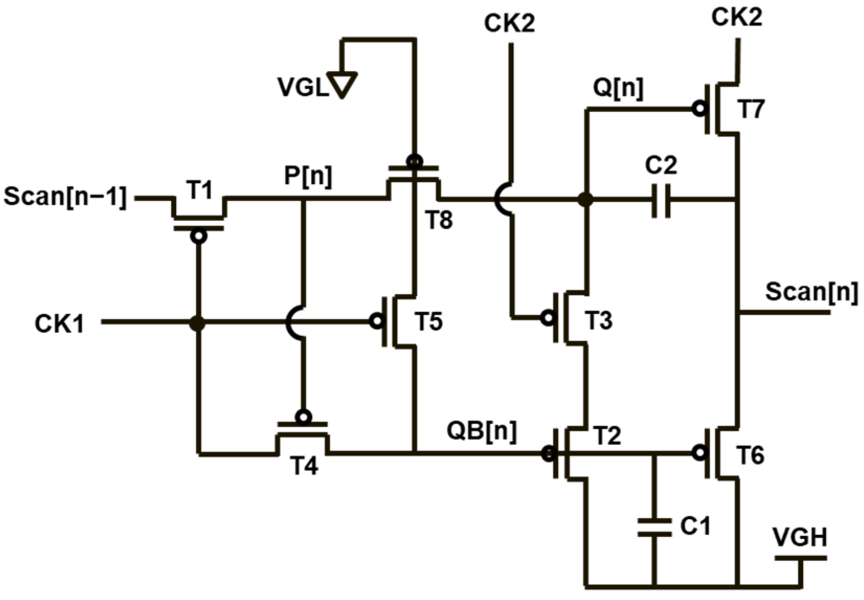
3. Proposed Scan Driver Circuit
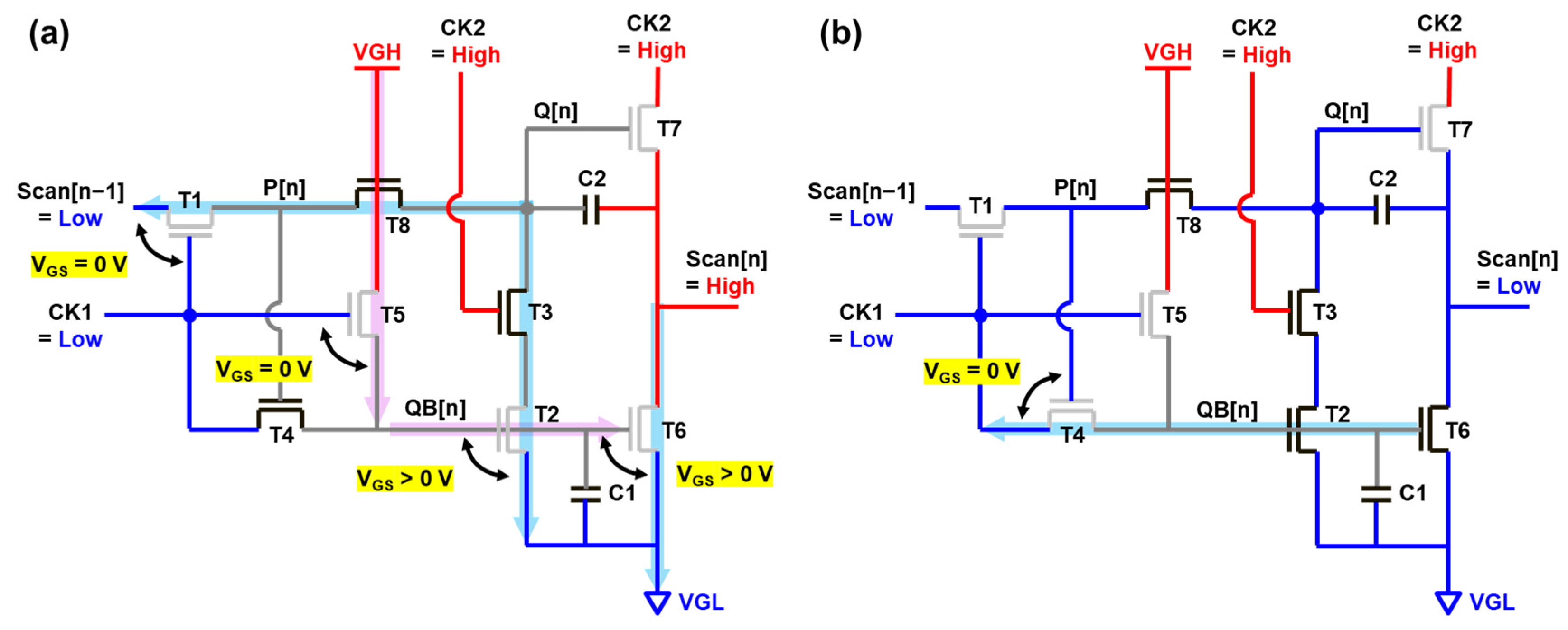
Figure 3 shows the schematic and the timing diagram of the proposed n-type MOx 10T-2C scan driver circuit. The circuit comprises ten TFTs and two capacitors. In comparison to the conventional MOx 8T-2C circuit, the proposed 10T-2C circuit has two more clock signals, i.e., CKL1 and CKL2. They have the same timing and the same high voltage level as CK1 and CK2, but the low voltage level is different. The low voltage level of CKL1 and CKL2 is VGLL, while that of CK1 and CK2 is VGL. VGLL is lower than VGL to cope with the depletion mode characteristics of MOx TFTs. In the 10T-2C scan driver circuit, the source voltage of every TFT is equal to VGL or higher. When CKL1 or CKL2 is applied to the gate node of the MOx TFT, it turns off completely even if its VTH is slightly negative, because VGS is lower than 0 V. Therefore, T1 is turned off completely during the output pull-up period and the Q[n] node voltage may rise reliably by effective bootstrapping. At the same time, the voltage of QB[n] maintains VGL because T5 is completely turned off by negative VGS. Therefore, the Scan[n] voltage can reach VGH more stably.
Two more TFTs, T9 and T10, are added to maintain the high voltage of QB[n] during the output hold-down period. Since T4 is turned off with the gate voltage of VGL, not VGLL, it may not turn off completely if VTH is negative. The two added TFTs, T9 and T10, make the source voltage of T4 VGH with the so-called series-connected two transistors (STT) configuration [12]. Accordingly, T4 can be turned off completely by negative VGS as shown in Figure 4. The overall operation of the proposed 10T-2C scan driver circuit in Figure 3 is as follows.

3.1. Pre-Charging

When CKL1 and Scan[n−1] are high, the P[n] and Q[n] nodes are pre-charged with a high voltage through T1. Since T3 is turned off by CKL2, the pre-charged voltage does not drop even if T3 has a slightly negative VTH. The QB[n] node maintains a high voltage during this period. Then, when CK1 and CKL1 become low before CK2 and CKL2 rise, the QB[n] voltage is discharged through T4 and T9, turning T6 off. At this moment, CKL1 turns off T1 completely even if T1 has a slightly negative VTH. Therefore, the pre-charged Q[n] voltage can be maintained by CKL1 and CKL2, which guarantees a stable bootstrapping operation and makes Scan[n] rise to VGH.

3.2. Output Pull-Up and Pull-Down

Next, CK2 rises to VGH, so the Q[n] voltage is boosted much higher than VGH by bootstrapping, e.g., exceeding the sum of VGH and VTH. This makes the Scan[n] voltage fully reach VGH. During this period, since T1 and T5 are stably turned off by CKL1, the bootstrapped high voltage Q[n] and discharged low voltage QB[n] are maintained respectively as they should be. Therefore, even if T6 has a slightly negative VTH, it does not pull-down Scan[n] significantly and T7 pulls up Scan[n] almost completely. Then, as CK2 goes down, Scan[n] is pulled down by T7.

3.3. Output Hold-Down

In order to hold-down Scan[n] stably, T6 should remain turned on after the pull-down operation. For this, T5 periodically connects the QB[n] node to VGH and the high QB[n] voltage is preserved by the STT configuration composed of T4, T9, and T10. In addition, T7 should not turn on when CK2 rises. However, when CK2 changes from VGL to VGH, the Q[n] node voltage might momentarily rise due to the capacitive coupling through gate-to-drain parasitic capacitance (CGD) of T7. This situation should be prevented by discharging the Q[n] node voltage to VGL through T2 and T3 when CK2 and CKL2 rise. However, in the conventional MOx 8T-2C scan driver circuit, T2 cannot be turned on strongly because the QB node is discharged through T4 if it has a negative VTH, as shown in Figure 2b. Therefore, T7 may slightly turn on, which leads to the undesirable fluctuation of the Scan[n] voltage. On the contrary, this situation is prevented by the STT configuration in the proposed 10T-2C scan driver circuit, even when T4 has negative VTH.

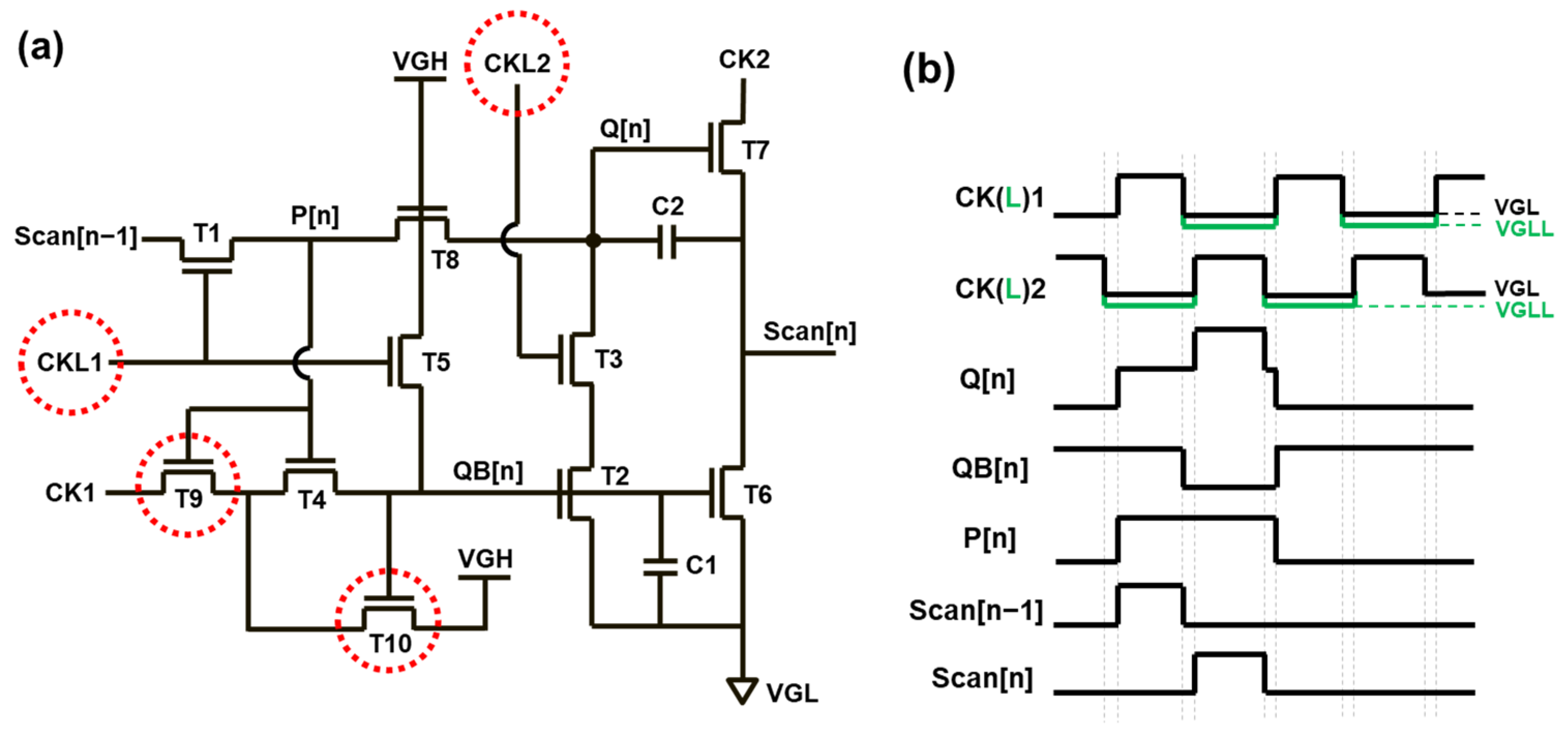
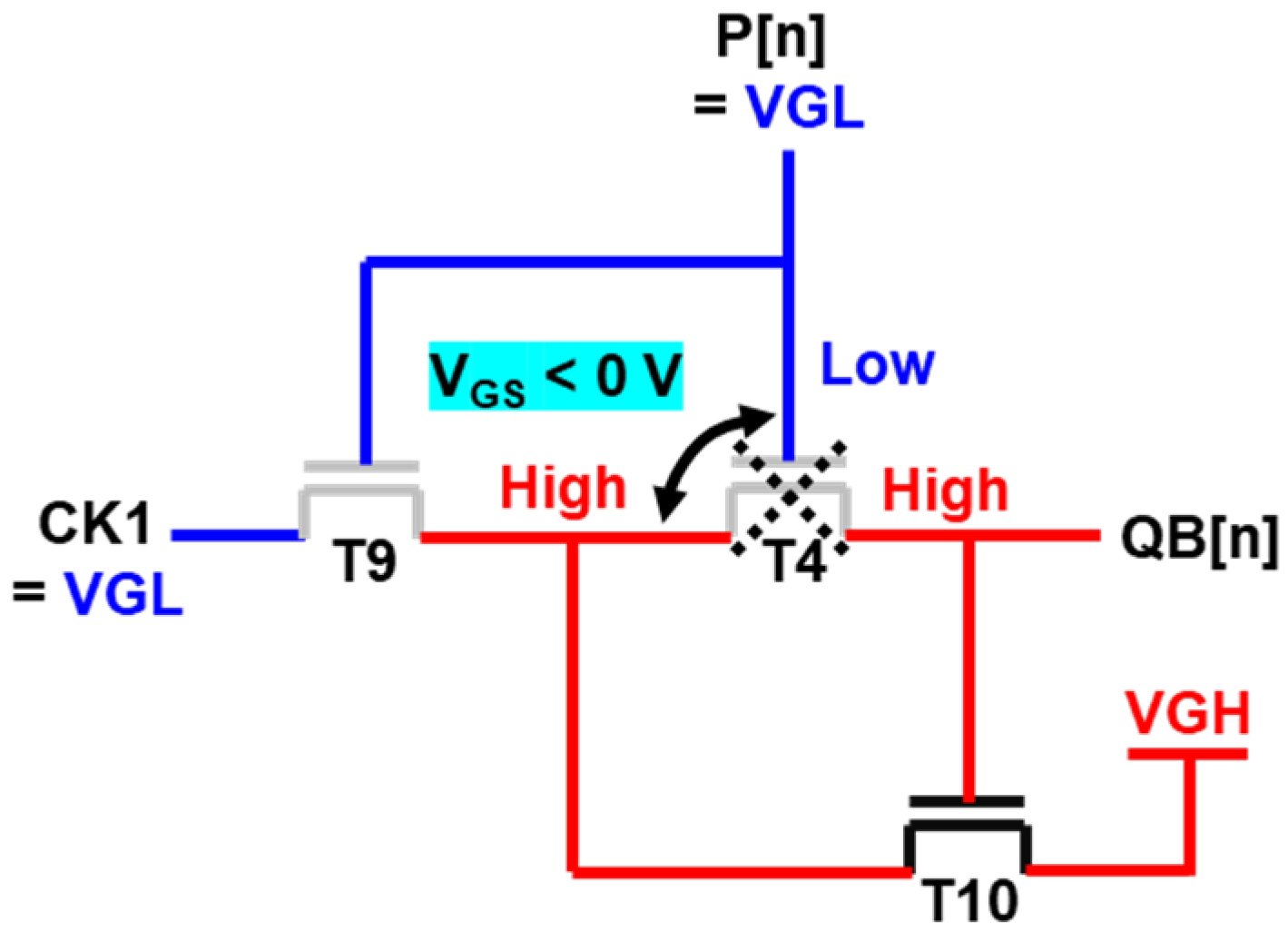
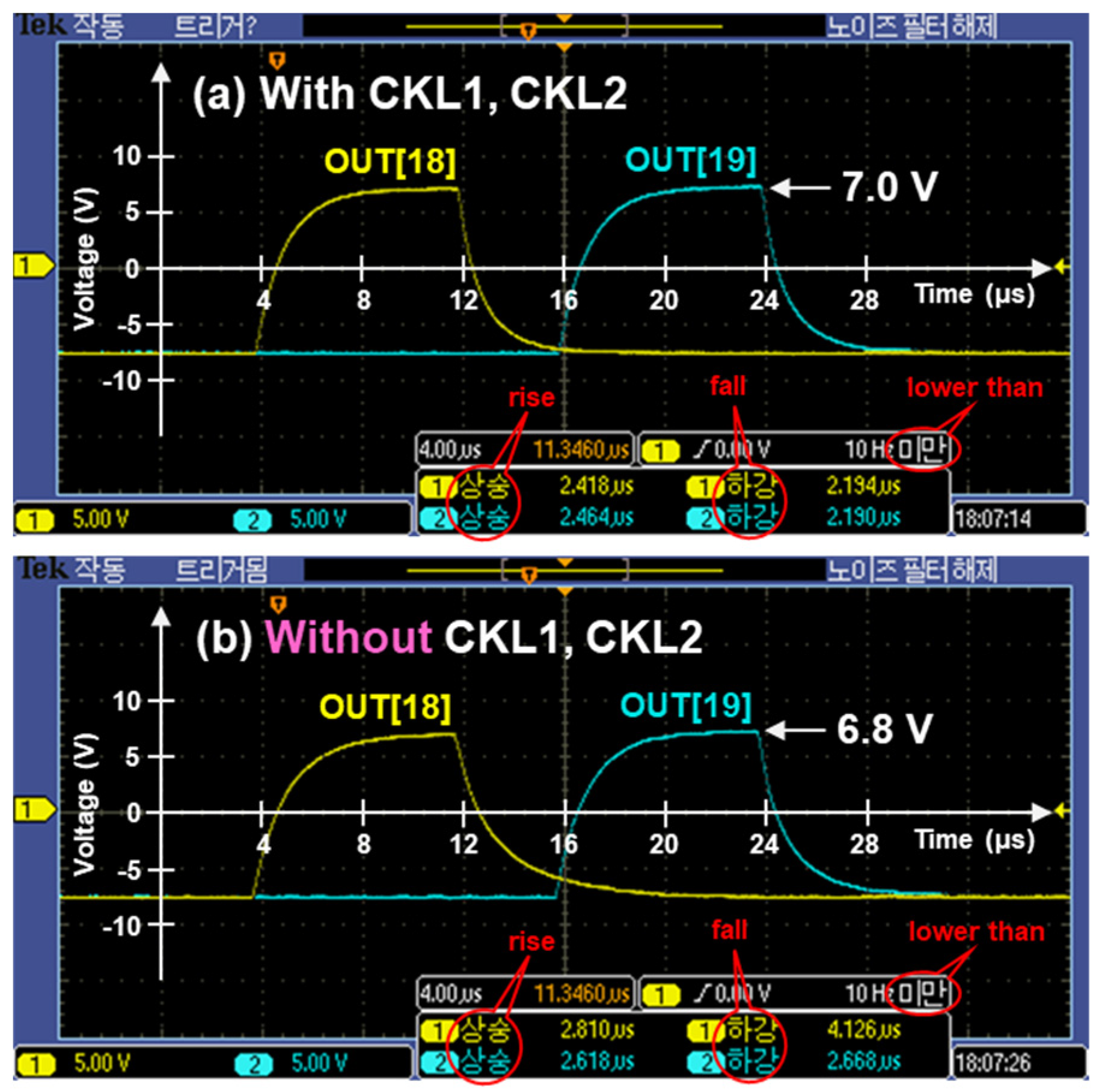
4. Results and Discussions

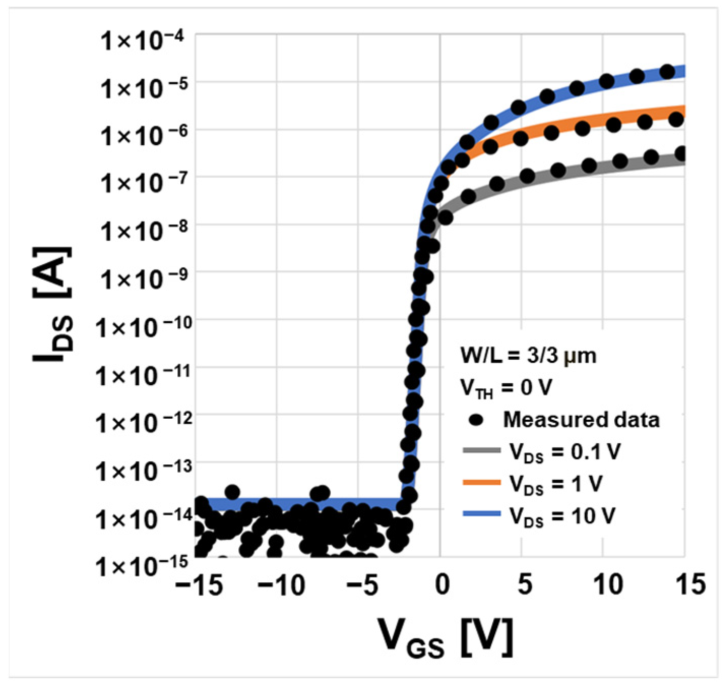
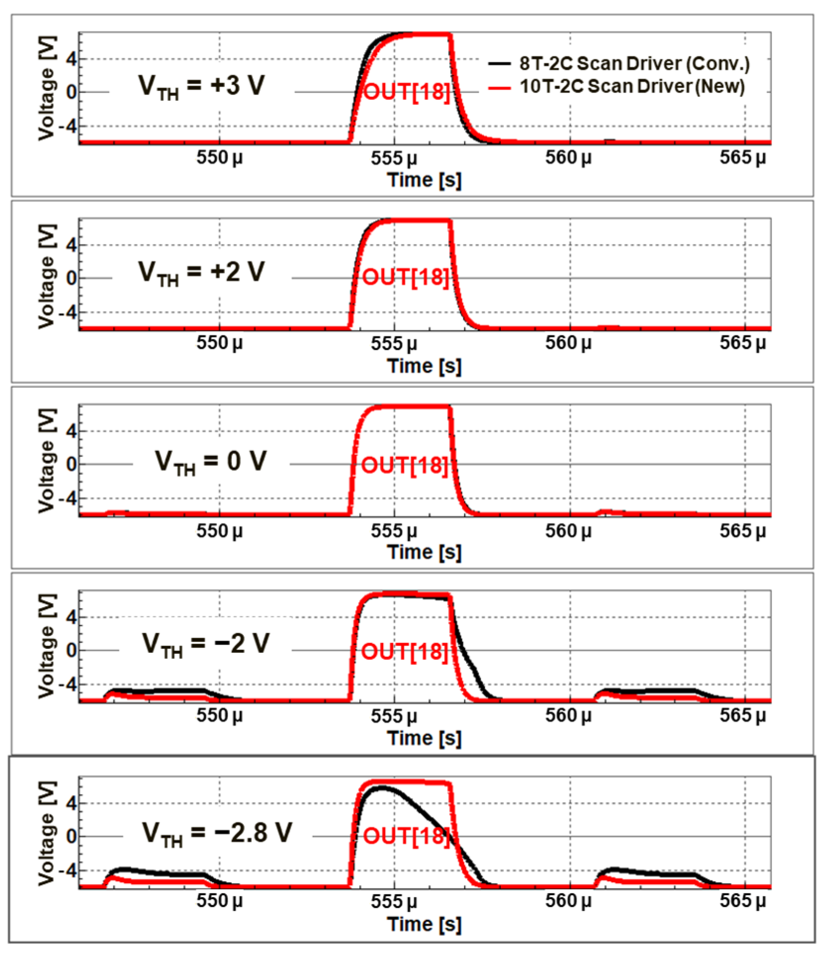
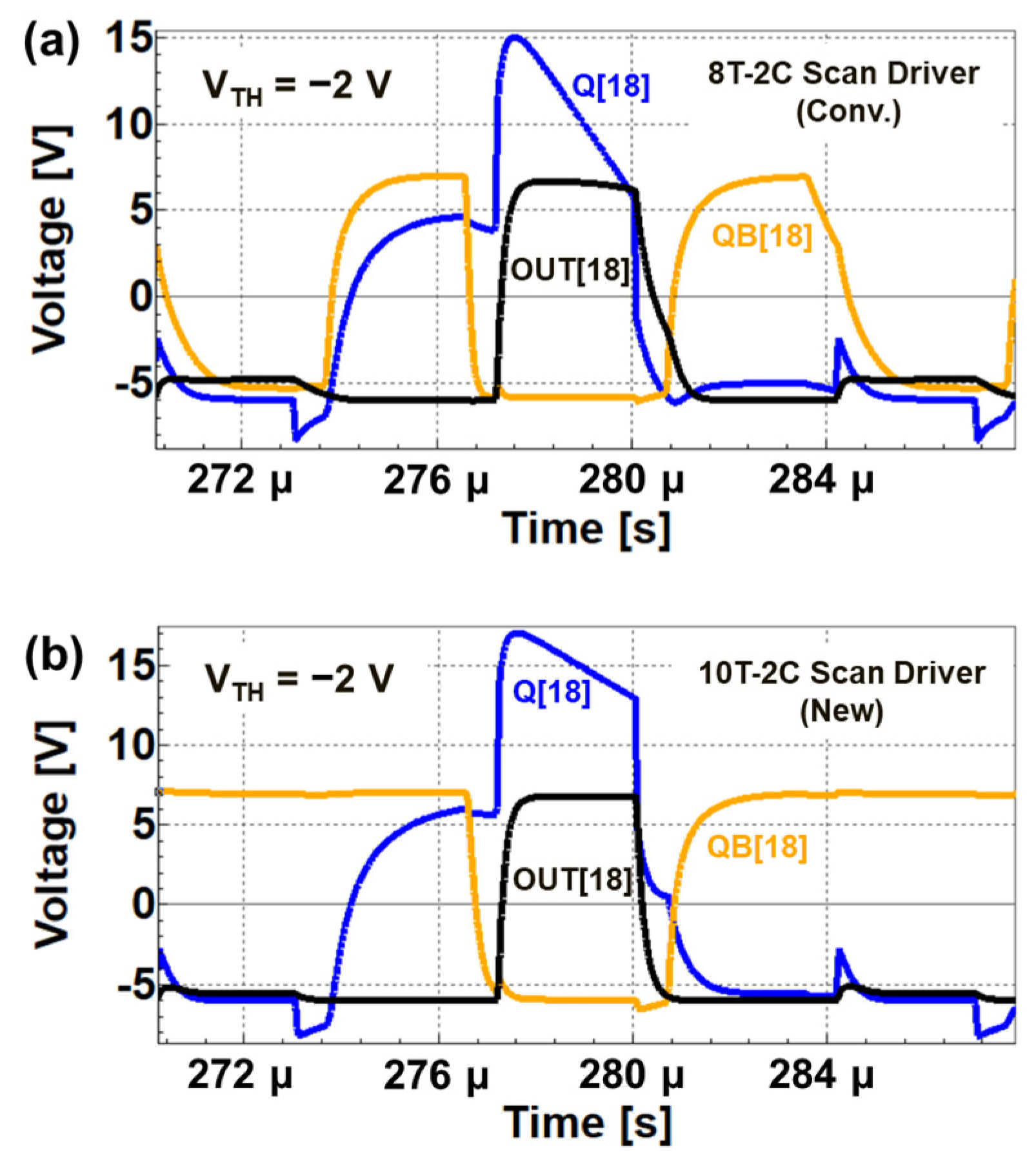
4.1. SPICE Simulation

The operation of the proposed 10T-2C scan driver circuit against VTH variation was verified by SPICE simulation using SmartSpice 5.4.0.R of Silvaco Inc. Figure 5 shows the measured transfer characteristics of n-type MOx TFT and its SPICE model when the drain-to-source voltage (VDS) is 0.1 V, 1 V, and 10 V. The RPI polysilicon TFT model of level = 36 was used and the model parameters such as VTO, MU0, MU1, MUS, ETA, etc. were modified to fit the measured device parameters such as VTH, carrier mobility, and subthreshold swing. The VTH of the SPICE model is 0 V and the off-current is about 10 fA regardless of VGS and VDS variation. The specifications of the 10T-2C circuit are listed in Table 1. The three voltage levels, VGH, VGL, and VGLL were selected as 7 V, −6 V, and −9 V, respectively. All TFTs have the same channel length (L) of 3 μm, but the channel width (W) varies according to the specific requirements for optimized circuit operation. The output buffer T7, responsible for both the pull-up and pull-down of the Scan[n] node, has the largest W of 400 μm. The capacitance of the C1 and C2 is same as 190 fF, and CLOAD and RLOAD attached to every Scan[n] node are 25 pF and 2 kΩ, respectively. The ideal pulse width of Scan[n], determined by the high-voltage duration of CK1/2, is set to 2.8 μs considering a commercial mobile AMOLED display with a vertical resolution of 3 K operating at a refresh rate of 120 Hz.
Figure 6 and Figure 7 show the SPICE simulation results of the conventional MOx 8T-2C scan driver circuit and the proposed MOx 10T-2C scan driver circuit for various VTH values. The test circuits for the SPICE simulation were composed of twenty stages of the unit circuit in Figure 3. The 18th output signals of the two circuits are shown in Figure 6. The black line is for the 8T-2C circuit, and the red line is for the 10T-2C circuit. When the VTH of every TFT in the circuits is between 0 V and +3 V, both circuits work normally. However, when the TFTs have depletion mode characteristics, the 10T-2C circuit considerably outperforms the 8T-2C circuit. It can be compared assuming the criteria of normal operation; for example, as the peak voltage of the output pulse is above 6.6 V—approximately 3% drop—and the fall time smaller than 500 ns. Applying these criteria, the operation margin of the 8T-2C circuit is only VTH ≥ −1 V. If VTH changes further in the negative direction, e.g., −2.8 V—the operation limit of 10T-2C circuit, the output pulse collapses as shown in Figure 6. The main reason of output pulse degradation is the leakage current through T1 which discharges the Q[n] node rapidly as illustrated in Figure 7a. As a result, T7 is turned off before the OUT[n] pull-down and the fall time increases, and the pulse height also degrades. On the contrary, for the proposed 10T-2C circuit, the operation margin is significantly improved to VTH ≥ −2.8 V. Since T1 is completely turned off with negative VGS and the Q[n] node voltage can be remained sufficiently high, the output pulse meets the criteria of normal operation even if VTH is −2.8 V.
During the output hold-down period, Scan[n] should maintain the VGL level. However, if VTH is below 0 V, T7 will turn on slightly and Scan[n] may fluctuate whenever CK2 rises. This problem becomes more serious due to the capacitive coupling through CGD of T7. To minimize the output voltage fluctuation, the Q[n] voltage should remain pulled down to VGL and QB[n] should be maintained at a high voltage when CK2 is high. However, in the conventional 8T-2C circuit, the QB[n] node is discharged through T4 as shown in Figure 7a, so T2 cannot sufficiently pull down the Q[n] node, which makes the Q[n] node more vulnerable to the capacitive coupling. Accordingly, a large output ripple appears as shown in Figure 6 and Figure 7a. On the contrary, in the proposed 10T-2C circuit, the QB[n] node maintains a high voltage as shown in Figure 7b owing to the STT structure composed of T4, T9 and T10. Therefore, the Q[n] voltage fluctuation is reduced, and the output voltage ripple is also reduced as shown in Figure 6 and Figure 7b. Our SPICE simulation results confirm that the proposed 10T-2C scan driver circuit operates stably over a wide VTH range of −2.8 V ≤ VTH ≤ +3.0 V.

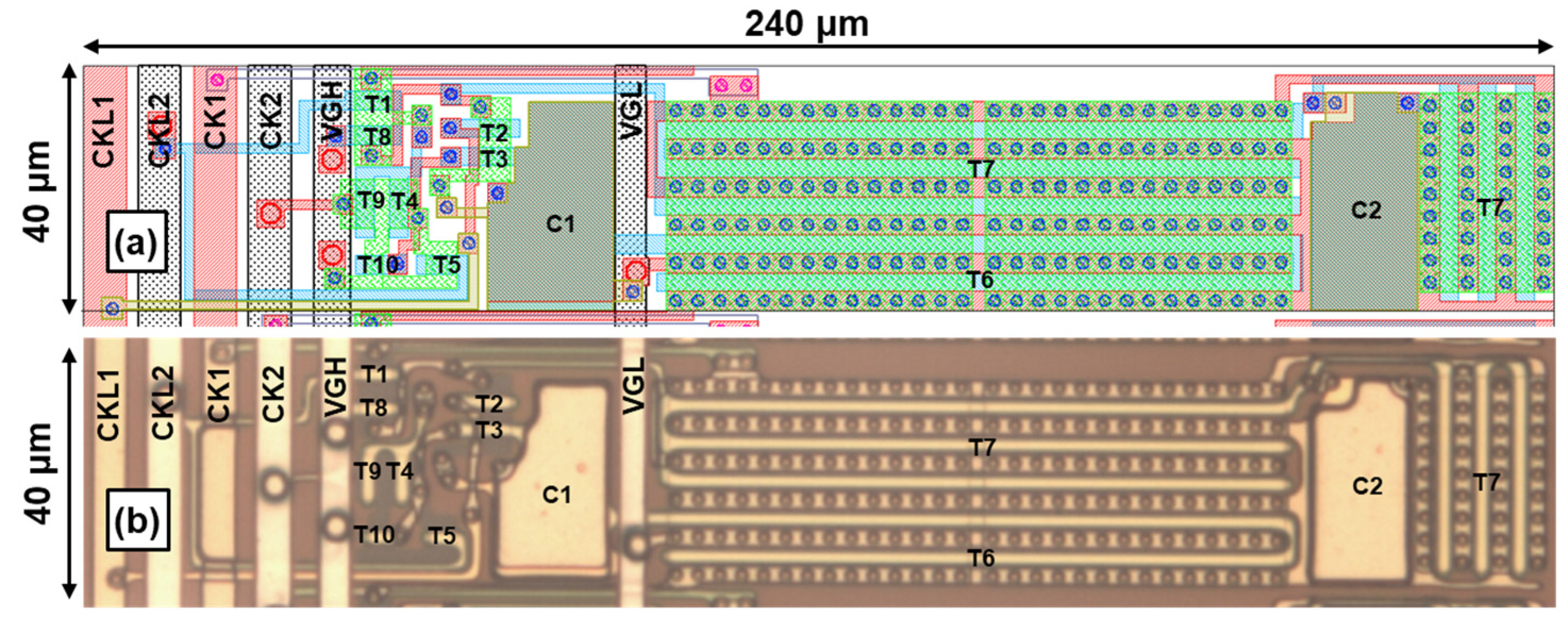
4.2. Fabrication and Measurement

A test sample of the proposed MOx 10T-2C scan driver circuit was fabricated to verify whether its area and performance are suitable for mobile displays. The MOx TFTs have top-gate coplanar structure with an amorphous indium-gallium-zinc-oxide (a-IGZO) channel layer and a SiO2 gate insulator. Molybdenum gate electrode and Ti/Al/Ti source/drain metal were used. The layout of the scan driver circuit was drawn according to the 2 μm design rule that is widely used in recent mobile AMOLED displays. Figure 8 shows the layout drawing and fabrication results of a unit stage circuit. The unit stage area is 40 μm × 240 μm assuming a 40 μm pixel pitch, i.e., 635 ppi. It should be noted that despite being composed only of MOx TFTs, the circuit area width is as small as 240 μm due to its simple structure. The performance of the test sample was evaluated using a probe station in a dark shielding box. The clock signals and supply voltages were generated by a pulse generator, EEC-P772 of ELP Corp, Republic of Korea. The output pulses were measured using an oscilloscope, MSO2024B of Tektronix, Inc.
The test sample has twenty stages cascaded and the operation conditions are listed in Table 1. Figure 9a shows the measured output signals of the 18th and the 19th stage. The peak of the output pulse is equal to a VGH of 7 V, as expected, and the low voltage level maintains a VGL of −6 V without ripple for 1 s. The rise and fall times are 2.4 μs and 2.2 μs, respectively. They are longer than the simulation results, possibly due to the large probing capacitance of the measurement system. In addition, instead of CKL1/2, we applied CK1/2 to the gate nodes of T1, T3, and T5 to check the effect of the lower-level clock signals. In this case, the peak of the output pulse does not reach VGH and the rise and fall times increase to 2.7 μs and 2.7 μs, respectively, as shown in Figure 9b. These results can be explained by two reasons: the poor bootstrapping and weak pull-down action of T7 due to the depletion mode characteristics of the MOx TFTs. Since the bootstrapped Q[n] node voltage is not maintained, the output pulse does not reach VGH and the rise and fall times increase compared with the results of Figure 9a. Therefore, it is confirmed that the lower-level clock signals, CKL1/2, are effective in overcoming the depletion mode characteristics of the MOx TFTs.
The purpose of this study is to devise an optimal solution that minimizes the area increase and to provide an acceptable device margin while considering the practical operation conditions of MOx TFT based-high-resolution mobile displays. Table 2 compares our proposed 10T-2C scan driver circuit with other previous scan driver circuits. The width of all previous circuits is wider than 500 μm, making it difficult to apply them to mobile displays with narrow bezels. On the other hand, the proposed 10T-2C scan driver circuit has the narrowest width of 240 μm owing to its simple structure consisting of only ten TFTs and two capacitors. In addition, the negative limit of TFT VTH is compared according to the criteria of normal operation described in Section 4.1. Typical VTH values of MOx TFTs vary from -1.0 V to 1.0 V depending on the manufacturing process conditions [15,16,17]. For a fair comparison, we set the operating voltages of the circuits to be the same, i.e., VGH = 7 V, VGL = −6 V, and VGLL = −9 V, respectively. The dimensions of the buffer TFTs and the output load conditions were also set to be the same. The simulation results show that the VTH limit of our 10T-2C circuit is as low as −2.8 V, while that of the previous circuits in Table 2 is −2.1 V [9], −0.9 V [13], and −0.4 V [14], respectively. In summary, our 10T-2C MOx TFT scan driver circuit is suitable for high-resolution mobile displays with a small bezel width and provides robustness against depletion mode MOx TFTs. However, the static current flow from VGH to VGL when the TFTs have negative VTH has not been completely solved in our circuit, and the power consumption may increase in proportion to the static current flow of the depletion mode MOx TFT. For example, when VTH is −0.5 V, −1.5 V, and −2.8 V, the power consumption of the proposed scan driver circuit composed of 3k stages and operated at 120 Hz frame rate, increases to 38.6 mW, 78.0 mW, and 147 mW, respectively.

5. Conclusions

We report a simple 10T-2C scan driver circuit suitable for a high-resolution mobile display, which overcomes the depletion mode characteristics of n-type MOx TFTs by employing lower-level clock signals and the STT configuration. SPICE simulation results show that its operation margin is the VTH range of −2.8 V ≤ VTH ≤ +3.0 V, which is a significantly improved performance compared with the conventional scan driver circuit that has a negative VTH limit of −2.1 V or higher. The fabricated circuit worked successfully, and the lower-level clock signals were proven to reduce the rise and fall times of the output signals. We expect that the proposed 10T-2C scan driver circuit suitable for the depletion mode characteristics of MOx TFTs can be utilized in high-resolution mobile AM displays, reducing the manufacturing cost.

Author Contributions

Conceptualization, Y.Y. and K.P.; methodology, Y.Y. and K.P.; software, Y.Y.; validation, Y.Y.; formal analysis, Y.Y.; investigation, Y.Y.; resources, K.P.; data curation, K.P.; writing—original draft preparation, Y.Y.; writing—review and editing, Y.Y. and K.P.; visualization, Y.Y. and K.P.; supervision, K.P.; project administration, K.P.; funding acquisition, J.L., K.S., J.K., Y.K., K.L. and K.C. All authors have read and agreed to the published version of the manuscript.

Funding

This research was supported by the Technology Innovation Program funded by the Ministry of Trade, Industry & Energy (MOTIE, Korea) [20016317], and the On-Panel Circuit Integration and Driving System Technology for 1270 ppi Low-Power OLED Display Based on Oxide Semiconductor.

Data Availability Statement

Data available in a publicly accessible repository.

Conflicts of Interest

Authors Junhyung Lim, Kyoungseok Son, Jaybum Kim, Youngoo Kim, Kyunghoe Lee, and Kyunghoon Chung were employed by the company Samsung Display Co., Ltd. The remaining authors declare that the research was conducted in the absence of any commercial or financial relationships that could be construed as a potential conflict of interest.

References

  1. Kunic, S.; Sego, Z. OLED Technology and Displays. In Proceedings of the 54th International Symposium ELMAR-2012, Zadar, Croatia, 12–14 September 2012; pp. 31–35. [Google Scholar]
  2. Chaji, R.; Nathan, A. Invited Paper: LTPS vs Oxide Backplanes for AMOLED Displays: System Design Considerations and Compensation Techniques. SID Int. Symp. Dig. Tech. Pap. 2014, 45, 153–156. [Google Scholar] [CrossRef]
  3. Park, K.-S.; Oh, S.; Yun, P.; Bae, J.U.; Kang, I.B. Invited Paper: Prospects of Oxide TFTs approaching LTPS. In Proceedings of the 2015 22nd International Workshop on Active-Matrix Flatpanel Displays and Devices (AM-FPD), Kyoto, Japan, 1–4 July 2015; pp. 241–244. [Google Scholar] [CrossRef]
  4. Ji, D.; Jang, J.; Park, J.H.; Kim, D.; Rim, Y.S.; Hwang, D.K.; Noh, Y.-Y. Recent progress in the development of backplane thin film transistors for information displays. J. Inf. Disp. 2021, 22, 1–11. [Google Scholar] [CrossRef]
  5. Kang, S.J.; Lee, H.S.; Woo, J.G.; Yu, E.S.; Lee, J.M.; Bae, B.S. Decoder-Type Scan Driver Suitable for Flexible and Stretchable Displays. Electronics 2022, 11, 519. [Google Scholar] [CrossRef]
  6. Lin, C.-L.; Lai, P.-C.; Chang, J.-H.; Chen, Y.-C.; Lai, P.-C.; Shih, L.-W. Reducing Leakage Current Using LTPS-TFT Pixel Circuit in AMOLED Smartwatch Displays. IEEE Trans. Ind. Electron. 2023, 70, 8588–8597. [Google Scholar] [CrossRef]
  7. Ke, J.; Deng, L.; Zhen, L.; Wu, Q.; Liao, C.; Luo, H.; Huang, S. An AMOLED Pixel Circuit Based on LTPS Thin-film Transistors with Mono-Type Scanning Driving. Electronics 2020, 9, 574. [Google Scholar] [CrossRef]
  8. Kim, K.-N.; Kang, J.-S.; Ahn, S.-J.; Lee, J.S.; Lee, D.H.; Kim, C.W.; Kwon, O.-K. A single-clock-driven gate driver using p-type, low-temperature polycrystalline silicon thin-film transistors. J. Inf. Disp. 2011, 12, 61–67. [Google Scholar] [CrossRef]
  9. Wu, Z.; Duan, L.; Yuan, G.; Jiang, C.; Li, Y.; Yan, L.; Cheng, J.; Wang, G.; Jin, S. An Integrated Gate Driver Circuit Employing Depletion-Mode IGZO TFTs. SID Int. Symp. Dig. Tech. Pap. 2012, 43, 5–7. [Google Scholar] [CrossRef]
  10. Han, I.; Song, E.; Kang, B.; Oh, K.; Kim, B.; Oh, C.; Ahn, B.; Nam, H. Depletion-Mode Oxide-TFT Shift Register with Wide Operating Frequency Range for AMOLED Displays. SID Int. Symp. Dig. Tech. Pap. 2015, 46, 61–63. [Google Scholar] [CrossRef]
  11. Song, R.; Wu, Y.; Lin, C.; Liu, K.; Qing, Z.; Li, Y.; Xue, Y. High-Speed Shift Register with Dual-Gated Thin-Film Transistors for a 31-Inch 4K AMOLED Display. Micromachines 2022, 13, 1696. [Google Scholar] [CrossRef] [PubMed]
  12. Kim, B.; Choi, S.C.; Lee, S.-Y.; Kuk, S.-H.; Jang, Y.H.; Kim, C.-D.; Han, M.-K. A Depletion-Mode a-IGZO TFT Shift Register With a Single Low-Voltage-Level Power Signal. IEEE Electron Device Lett. 2011, 32, 1092–1094. [Google Scholar] [CrossRef]
  13. Iwase, Y.; Tagawa, A.; Takeuchi, Y.; Watanabe, T.; Horiuchi, S.; Asai, Y.; Yamamoto, K.; Daitoh, T.; Matsuo, T. A novel low-power gate driver architecture for large 8 K 120 Hz liquid crystal display employing IGZO technology. J. Soc. Inf. Disp. 2018, 26, 304–313. [Google Scholar] [CrossRef]
  14. Tu, C.-D.; Tsao, S.-W.; Huang, C.-H.; Yu, W.-S.; Chen, Y.-C.; Lee, M.-H.; Hong, K.-W.; Chang, H.-S.; Lee, S.-C.; Kuo, C.-H. A Gate Driver Circuit with a-IGZO TFTs for 8-inch QXGA TFT-LED Panel. J. Soc. Inf. Disp. 2017, 48, 1416–1418. [Google Scholar] [CrossRef]
  15. Xu, P.; Han, Y.; Zhang, H.; Liu, F.; Yan, G.; Zhu, M.; Wang, L.; Zhao, D.; Zhang, X.; Luo, C.; et al. Development of Internal Compensation Technology for Medium Size OLED Display based on Oxide TFTs. SID Int. Symp. Dig. Tech. Pap. 2024, 37–40. [Google Scholar]
  16. Yan, G.; Wang, D.; Ding, L.; Xu, L.; Sun, X.; Chen, F.-H.; Xing, R.; Li, J. Development of High Mobility and Reliability Metal Oxide TFT for 13.2 inch AMOLED Display. SID Int. Symp. Dig. Tech. Pap. 2024, 154–157. [Google Scholar]
  17. Ning, C.; Wang, D.; Yuan, G.; Wang, L.; Liu, F.; Sun, H.; Lu, Y.; He, J.; Ma, Y.; Lin, Y. Ultra-low power consumption notebook LCD with high on-state current metal oxide device. SID Int. Symp. Dig. Tech. Pap. 2024, 1448–1451. [Google Scholar]
Figure 1. Schematic of the conventional p-type LTPS 8T-2C scan driver circuit.
Electronics 13 02254 g001
Figure 2. Incomplete turn-off cases of n-type MOx TFT in conventional 8T-2C scan driver circuit due to its depletion-mode characteristics, which result in circuit operation error. (a) During output pull-up period and (b) during output hold-down period.
Electronics 13 02254 g002
Figure 3. (a) Schematic and (b) timing diagram of the proposed n-type MOx 10T-2C scan driver circuit.
Electronics 13 02254 g003
Figure 4. Operation principle of the series-connected two-transistor (STT) configuration in the proposed 10T-2C scan driver circuit.
Electronics 13 02254 g004
Figure 5. Measured transfer characteristics of n-type MOx TFT and SPICE model with VDS variation from 0.1 V to 10 V when VTH = 0 V.
Electronics 13 02254 g005
Figure 6. Comparison of SPICE simulation results of the conventional MOx 8T-2C scan driver circuit and the proposed MOx 10T-2C scan driver circuit over a wide VTH variation range of −2.8 V ≤ VTH ≤ +3.0 V.
Electronics 13 02254 g006
Figure 7. SPICE simulation results of (a) the conventional MOx 8T-2C scan driver circuit, and (b) the proposed MOx 10T-2C scan driver circuit when VTH = −2 V.
Electronics 13 02254 g007
Figure 8. (a) Layout drawing and (b) micrograph showing the unit stage of the proposed MOx 10T-2C scan driver circuit.
Electronics 13 02254 g008
Figure 9. Measured output signals of the proposed MOx 10T-2C scan driver circuit.
Electronics 13 02254 g009
Table 1. Design parameters of the proposed 10T-2C scan driver circuit.
ParameterValue
VGH7 V
VGL−6 V
VGLL−9 V
CK1, CK27 V/−6 V
CKL1, CKL27 V/−9 V
W/L of T6200/3 μm
W/L of T7400/3 μm
W/L of T1, T86/3 μm
W/L of T2, T3, T55/3 μm
W/L of T4, T98/3 μm
W/L of T102/3 μm
C1, C2190 fF
CLOAD25 pF
RLOAD2 kΩ
Table 2. Comparison of the proposed 10T-2C scan driver circuit with previous scan driver circuits.
ReferenceTFT TypeStructureWidth of Scan
Driver Circuit
Negative Limit
of TFT VTH
[9]n-type a-IGZO15T-1C1200 μm−2.1 V
[13]n-type a-IGZO11T-1C3500 μm−0.9 V
[14]n-type a-IGZO15T-1C1000 μm−0.4 V
This work n-type a-IGZO10T-2C240 μm−2.8 V
Disclaimer/Publisher’s Note: The statements, opinions and data contained in all publications are solely those of the individual author(s) and contributor(s) and not of MDPI and/or the editor(s). MDPI and/or the editor(s) disclaim responsibility for any injury to people or property resulting from any ideas, methods, instructions or products referred to in the content.

