
Challenges: ESD Protection for Heterogeneously Integrated SoICs in Advanced Packaging


Abstract
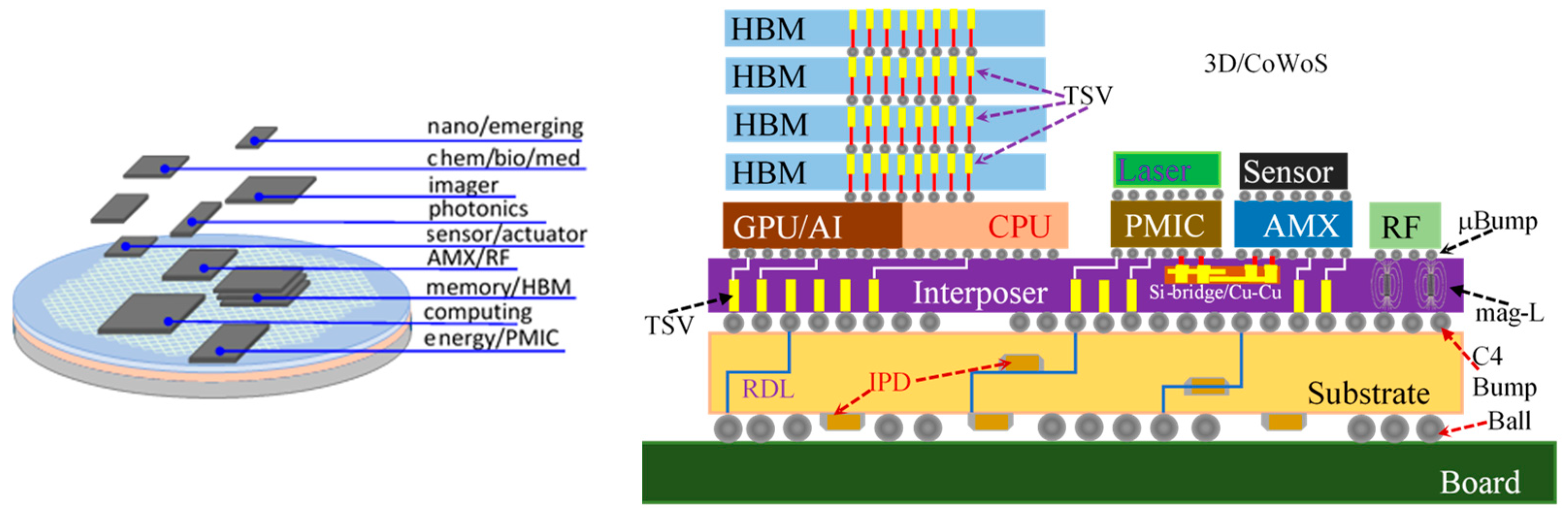
:1. Introduction
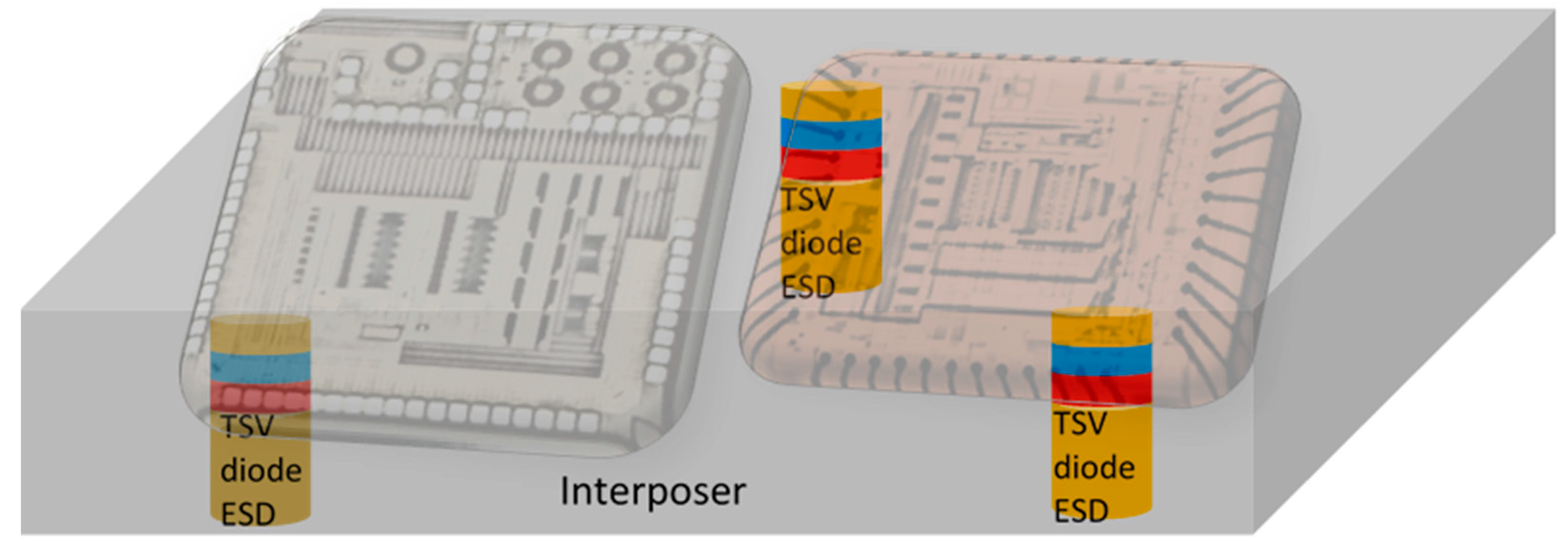
2. Holistic ESD Protection for SoICs
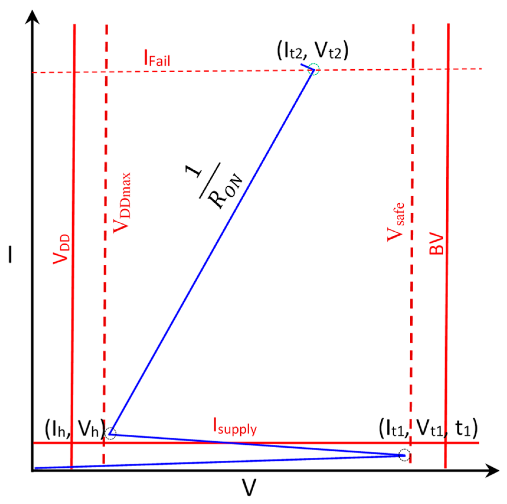
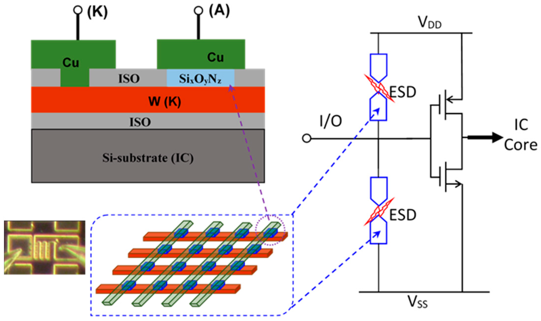
3. CDM ESD Protection for SoICs
4. SoIC ESD Modeling and Simulation Challenges
5. Summary
Author Contributions
Funding
Data Availability Statement
Conflicts of Interest
References
- Brattain, W.H. Entry of 15 December 1947, Laboratory Notebook, Case 38139-7; Bell Laboratories Archives: Murray Hill, NJ, USA, 1947. [Google Scholar]
- Shockley, W. Circuit Element Utilizing Semiconductor Material. U.S. Patent 2,569,347A, 25 September 1951. [Google Scholar]
- Shockley, W. Semiconductor Amplifier. U.S. Patent 2,502,488A, 4 April 1950. [Google Scholar]
- Kilby, J.S. Miniaturized Electronic Circuits. U.S. Patent 3,138,743, 23 June 1964. [Google Scholar]
- Moore, G.E. Cramming more components onto integrated circuits. Electronics 1965, 38, 114–117. [Google Scholar] [CrossRef]
- Li, C.; Pan, Z.; Li, X.; Hao, W.; Miao, R.; Wang, A. Selective Overview of 3D Heterogeneity in CMOS. Nanomaterials 2022, 12, 2340. [Google Scholar] [CrossRef] [PubMed]
- Bhattacharya, R.; Han, J.W.; Browning, J.; Meyyappan, M. Complementary vacuum field emission transistor. IEEE Trans. Electron Devices 2021, 68, 5244–5249. [Google Scholar] [CrossRef]
- Shen, Y.; Harris, N.; Skirlo, S.; Prabhu, M.; Baehr-Jones, T.; Hochberg, M.; Sun, X.; Zhao, S.; Larochelle, H.; Englund, D.; et al. Deep learning with coherent nanophotonic circuits. Nat. Photonics 2017, 11, 441. [Google Scholar] [CrossRef]
- Zhu, J.; Cheng, H. Recent development of flexible and stretchable antennas for bio-integrated electronics. Sensors 2018, 18, 4364. [Google Scholar] [CrossRef]
- Behin-Aein, B.; Datta, D.; Salahuddin, S.; Datta, S. Proposal for an all-spin logic device with built-in memeory. Nat. Nanotech. 2010, 5, 266. [Google Scholar] [CrossRef]
- Geng, Z.; Hähnlein, B.; Granzner, R.; Auge, M.; Lebedev, A.A.; Davydov, V.Y.; Kittler, M.; Pezoldt, J.; Schwierz, F. Graphene nanoribbons for electronic devices. Ann. Phys. 2017, 529, 1700033. [Google Scholar] [CrossRef]
- Schwierz, F. Graphene transistors: Status, prospects, and problems. Proc. IEEE 2013, 101, 1567–1584. [Google Scholar] [CrossRef]
- Yang, S.; Jiang, C.; Wei, S.-H. Gas sensing in 2D materials. Appl. Phys. Rev. 2017, 4, 021304. [Google Scholar] [CrossRef]
- Wei, H.; Shulaker, M.; Wong, H.S.P.; Mitra, S. Monolithic three-dimensional integration of carbon nanotube FET complementary logic circuits. In Proceedings of the IEEE Technical Digest—International Electron Devices Meeting, Washington, DC, USA, 9–11 December 2013. [Google Scholar]
- Shulaker, M.M.; Hills, G.; Park, R.S.; Howe, R.T.; Saraswat, K.; Wong, H.-S.P.; Mitra, S. Three-dimensional integration of nanotechnologies for computing and data storage on a single chip. Nature 2017, 547, 74–78. [Google Scholar] [CrossRef]
- Fuchs, E.R.H.; Bruce, E.J.; Ram, R.J.; Kirchain, R.E. Process-Based Cost Modeling of Photonics Manufacture: The Cost Competitiveness of Monolithic Integration of a 1550-nm DFB Laser and an Electroabsorptive Modulator on an InP Platform. IEEE J. Light. Technol. 2006, 24, 3175–3186. [Google Scholar] [CrossRef]
- Zou, P.; Xie, Q.; Song, W.; Jiang, Q.; Lu, Y.; Huang, B. Powering 5G Era Computing Platforms—The Road toward Integrated Power Delivery. In Proceedings of the IEEE International Symposium on Power Semiconductor Devices and ICs (ISPSD), Shanghai, China, 19–23 May 2019. [Google Scholar]
- Lerner, R.; Eisenbrandt, S.; Bower, C.; Bonafede, S.; Fecioru, A.; Reiner, R.; Waltereit, P. Integration of GaN HEMTs onto Silicon CMOS by Micro Transfer Printing. In Proceedings of the IEEE International Symposium on Power Semiconductor Devices and ICs, Prague, Czech Republic, 12–16 June 2016. [Google Scholar]
- Qi, Z.; Zhao, C.; Wang, L.; Yang, F.; Pei, Y.; Zheng, Z. Three-Dimensional Integrated GaN-based DC-DC Converter with an Inductor Substrate. In Proceedings of the IEEE Energy Conversion Congress and Exposition (ECCE), Baltimore, MD, USA, 29 September–3 October 2019; pp. 832–838. [Google Scholar]
- Besancon, C.; Neel, D.; Ramirez, J.; Bitauld, D.; Cerulo, G.; Make, D.; Vaissiere, N.; Pommereau, F.; Founel, F.; Sanchez, L.; et al. AlGaInAs MQW Laser Regrowth on Heterogenerous InP-on-SOI: Performance for Different Silicon Cavity Designs. In Proceedings of the IEEE Optical Fiber Communications Conference and Exhibition (OFC), San Francisco, CA, USA, 6–10 June 2021. [Google Scholar]
- LaPedus, M. 5 nm vs. 3 nm. Semiconductor Engineering. Gartner Report. 2019. Available online: https://semiengineering.com/5nm-vs-3nm/ (accessed on 1 March 2024).
- Graef, M. More Than Moore White Paper. In Proceedings of the International Roadmap for Devices and Systems Outbriefs, Santa Clara, CA, USA, 30 November 2021. [Google Scholar]
- ITRS. International Technology Roadmap for Semiconductors 2.0. 2015 Edition. Available online: http://www.itrs2.net/ (accessed on 1 March 2024).
- Chen, M.-F.; Chen, F.-C.; Chiou, W.-C.; Yu, D.C.H. System on Integrated Chips (SoIC) for 3D Heterogeneous Integration. In Proceedings of the IEEE Electronic Components and Technology Conference (ECTC), Las Vegas, NV, USA, 28–31 May 2019; pp. 594–599. [Google Scholar]
- HIR. Heterogeneous Integration Roadmap. IEEE Electronics Packaging Society. Available online: https://eps.ieee.org/technology/heterogeneous-integration-roadmap.html (accessed on 1 March 2024).
- CoWoS. TSMC. Available online: https://3dfabric.tsmc.com/english/dedicatedFoundry/technology/cowos.htm (accessed on 1 March 2024).
- Banijamali, B.; Chiu, C.-C.; Hsieh, C.-C.; Lin, T.-S.; Hu, C.; Hou, S.-Y.; Ramalingam, S.; Jeng, S.-P.; Madden, L.; Yu, D.C.H. Reliability evaluation of a CoWoS-enabled 3D IC package. In Proceedings of the IEEE Electronic Components and Technology Conference, Las Vegas, NV, USA, 28–31 May 2013; pp. 35–40. [Google Scholar]
- NVIDIA GDX B200. Available online: https://www.nvidia.com/en-us/data-center/dgx-b200/ (accessed on 1 March 2024).
- Pan, Z.; Li, X.; Hao, W.; Miao, R.; Wang, A. Design for EMI/ESD Immunity for Flexible and Wearable Electronics. IEEE J. Electron Devices Soc. (J-EDS) 2023, 11, 700–707. [Google Scholar] [CrossRef]
- Liang, S.W.; Liang, Y.R.; Wu, G.C.Y.; Yee, K.C.; Wang, C.T.; Yu, D.C.H. Reliability Performance on Fine-Pitch SoI Bond. In Proceedings of the IEEE Electronic Components and Technology Conference (ECTC), Orlando, FL, USA, 30 May–2 June 2023; pp. 783–787. [Google Scholar]
- Lu, R.; Chuang, Y.-C.; Wu, J.-L.; He, J. Reliability Challenges from 2.5D to 3DIC in Advanced Package Development. In Proceedings of the IEEE International Reliability Physics Symposium (IRPS), Monterey, CA, USA, 26–30 March 2023. [Google Scholar]
- Pan, Z.; Li, C.; Hao, W.; Li, X.; Wang, A. ESD Protection Designs: Topical Overview and Perspective. IEEE Trans. Device Mater. Reliab. 2022, 22, 356–370. [Google Scholar] [CrossRef]
- Simicic, M.; Gijbels, F.; Iacovo, S.; Chen, S.-H.; Van Der Plas, G.; Beyne, E. ESD process assessment of 2.5D and 3D bonding technologies. In Proceedings of the IEEE EOS/ESD Symposium (EOS/ESD), Riverside, CA, USA, 2–4 October 2023. [Google Scholar]
- TSMC CoWoS Packaging. Available online: https://en.wikichip.org/wiki/tsmc/cowos (accessed on 1 March 2024).
- Gartner Says Worldwide Semiconductor Revenue Grew 1.1% in 2022. Gartner Pres Release, 1/17/2023. Available online: https://www.gartner.com/en/newsroom/press-releases/2023-01-17-gartner-says-worldwide-semiconductor-revenue-grew-one-percent-in-2022 (accessed on 1 March 2024).
- Global Semiconductors Market Size to Exceed USD 1123.44 Billion By 2033|CAGR Of 6.27%, 4/16/2024. Available online: https://finance.yahoo.com/news/global-semiconductors-market-size-exceed-153000484.html (accessed on 1 March 2024).
- Voldman, S. ESD: RF Technology and Circuits; Wiley: Hoboken, NJ, USA, 2006; ISBN -13: 978-0470847558. [Google Scholar]
- Wang, A. Practical ESD Protection Design; Wiley-IEEE Press: New York, NY, USA, 2022; ISBN -13 978-1119850403. [Google Scholar]
- Pan, Z.; Li, X.; Hao, W.; Miao, R.; Wang, A. On-Chip ESD Protection Design Methodologies by CAD Simulation. ACM Trans. Des. Autom. Electron. Syst. 2023, 29, 4. [Google Scholar] [CrossRef]
- Di, M.; Li, C.; Pan, Z.; Wang, A. Non-Pad-Based in Situ in-Operando CDM ESD Protection Using Internally Distributed Network. IEEE J. Electron Devices Soc. 2021, 9, 1248–1256. [Google Scholar] [CrossRef]
- Wang, A. ESD Protection Structures and Local Grounding Using Through-Silicon-Vias (TSV) for ICs. U.S. Patent (filed) # 62/385,770, 9 September 2016. [Google Scholar]
- Wang, A. Interposer-based ESD Protection Structures. U.S. Patent (pending) #62/412,105, 2016. [Google Scholar]
- Wang, A. Nano Crossbar ESD Protection Circuits, Devices and Structures. U.S. Patent (pending) # 61/147,561, 2009. [Google Scholar]
- Wang, L.; Wang, X.; Shi, Z.; Ma, R.; Liu, J.; Dong, Z.; Zhang, C.; Lin, L.; Zhao, H.; Zhang, L.; et al. Dual-Directional Nano Crossbar Array ESD Protection Structures. IEEE Electron Device Lett. 2013, 34, 111–113. [Google Scholar] [CrossRef]
- Di, M.; Li, C.; Pan, Z.; Wang, A. Pad-Based CDM ESD Protection Methods Are Faulty. IEEE J. Electron Devices Soc. 2020, 8, 1297–1304. [Google Scholar] [CrossRef]
- JESD22-C101-A; Field-Induced Charged-Device Model Test Method for Electrostatic Discharge-Withstand Thresholds of Microelectronic Components, the Electronics Industries Alliance. JEDEC: Arlington, VA, USA, 2000.
- ANSI/ESDA/JEDEC JS-002-2018; For Electrostatic Discharge Sensitivity Testing—Charged Device Model (CDM)—Device Level, An American National Standard jointly developed by ESD Association and JEDEC. JEDEC: Arlington, VA, USA, 2018.
- ESD TR5.5-03-14; ESD Association Technical Report for Electrostatic Discharge (ESD) Sensitivity Testing—Very Fast—Transmission Line Pulse (TLP)—Round Robin Analysis. ESD Association Standard Practice for Electrostatic Discharge Sensitivity Testing—Human Metal Model (HMM) Component Level. ESD: Rome, NY, USA, 2014.
- MIL-STD-883E; Method 3015.7, Electrostatic Discharge Sensitivity Classification. Department of Defense, Test Method Standard. Microcircuits: Washington, DC, USA, 1989.
- ANSI/ESDA/JEDEC JS-001-2017; For Electrostatic Discharge Sensitivity Testing—Human Body Model (HBM)—Component Level, An American National Standard Jointly Developed by ESD Association and JEDEC. JEDEC: Arlington, VA, USA, 2017.
- Barth, J.; Verhaege, K.; Henry, L.; Richner, J. TLP Calibration, Correlation, Standards, and New Techniques. In Proceedings of the EOS/ESD Symposium, Anaheim, CA, USA, 26–28 September 2000; pp. 85–96. [Google Scholar]
- Zhang, F.; Wang, C.; Lu, F.; Chen, Q.; Li, C.; Wang, X.S.; Li, D.; Wang, A. A Full-Chip ESD Protection Circuit Simulation and Fast Dynamic Checking Method Using SPICE and ESD Behavior Models. IEEE Trans. Comput.-Aided Des. Integr. Circuits Syst. 2019, 38, 489–498. [Google Scholar] [CrossRef]
- Feng, H.; Chen, G.; Zhan, R.; Wu, Q.; Guan, X.; Xie, H.; Wang, A.; Gafiteanu, R. A Mixed-Mode ESD Protection Circuit Simulation-Design Methodology. IEEE J. Solid-State Circuits 2003, 38, 995–1006. [Google Scholar] [CrossRef]
- Lu, F.; Ma, R.; Dong, Z.; Wang, L.; Zhang, C.; Wang, C.; Chen, Q.; Wang, X.S.; Zhang, F.; Li, C.; et al. A Systematic Study of ESD Protection Co-Design with High-Speed and High-Frequency ICs in 28 nm CMOS. IEEE Trans. Circuits Syst. I Regul. Pap. 2016, 63, 1746–1757. [Google Scholar] [CrossRef]
- Wang, L.; Wang, X.; Shi, Z.T.; Ma, R.; Zhang, C.; Dong, Z.; Lu, F.; Zhao, H.; Wang, A. Scalable Behavior Modeling for 3D Field-Programmable ESD Protection Structures. In Proceedings of the IEEE CICC, San Jose, CA, USA, 22–25 September 2013. [Google Scholar]
- Zhan, R.; Feng, H.; Wu, Q.; Wang, A. ESDExtractor: A New Technology-Independent CAD Tool for Arbitrary ESD Protection Device Extraction. IEEE Trans. Comput.-Aided Des. Integr. Circuits Syst. 2003, 22, 1362–1370. [Google Scholar] [CrossRef]
- Zhan, R.; Feng, H.; Wu, Q.; Xie, H.; Guan, X.; Chen, G.; Wang, A. ESDInspector: A New Layout-level ESD Protection Circuitry Design Verification Tool Using a Smart-Parametric Checking Mechanism. IEEE Trans. Comput.-Aided Des. Integr. Circuits Syst. 2004, 23, 1421–1428. [Google Scholar] [CrossRef]


Disclaimer/Publisher’s Note: The statements, opinions and data contained in all publications are solely those of the individual author(s) and contributor(s) and not of MDPI and/or the editor(s). MDPI and/or the editor(s) disclaim responsibility for any injury to people or property resulting from any ideas, methods, instructions or products referred to in the content. |
© 2024 by the authors. Licensee MDPI, Basel, Switzerland. This article is an open access article distributed under the terms and conditions of the Creative Commons Attribution (CC BY) license (https://creativecommons.org/licenses/by/4.0/).
Share and Cite
Pan, Z.; Li, X.; Hao, W.; Miao, R.; Yue, Z.; Wang, A. Challenges: ESD Protection for Heterogeneously Integrated SoICs in Advanced Packaging. Electronics 2024, 13, 2341. https://doi.org/10.3390/electronics13122341
Pan Z, Li X, Hao W, Miao R, Yue Z, Wang A. Challenges: ESD Protection for Heterogeneously Integrated SoICs in Advanced Packaging. Electronics. 2024; 13(12):2341. https://doi.org/10.3390/electronics13122341
Chicago/Turabian StylePan, Zijin, Xunyu Li, Weiquan Hao, Runyu Miao, Zijian Yue, and Albert Wang. 2024. "Challenges: ESD Protection for Heterogeneously Integrated SoICs in Advanced Packaging" Electronics 13, no. 12: 2341. https://doi.org/10.3390/electronics13122341