Article

Innovative Programming Approaches to Address Z-Interference in High-Density 3D NAND Flash Memory

Department of Semiconductor Engineering, Seoul National University of Science & Technology, Seoul 01811, Republic of Korea
*
Author to whom correspondence should be addressed.
Electronics 2024, 13(16), 3123; https://doi.org/10.3390/electronics13163123
Submission received: 30 June 2024 / Revised: 22 July 2024 / Accepted: 6 August 2024 / Published: 7 August 2024
(This article belongs to the Special Issue Advanced Non-Volatile Memory Devices and Systems)

Abstract

:
Increasing the bit density in 3D NAND flash memory involves reducing the pitch of ON (Oxide-Nitride) molds in the Z-direction. However, this reduction drastically increases Z-interference, adversely affecting cell distribution and accelerating degradation of reliability limits. Previous studies have shown that programming from the top word line (WL) to the bottom WL, instead of the traditional bottom-to-top approach, alleviates Z-interference. Nevertheless, detailed analysis of how Z-interference varies at each WL depending on the programming sequence remains insufficient. This paper investigates the causes of Z-interference variations at Top, Middle, and Bottom WLs through TCAD analysis. It was found that as more electrons are programmed into WLs within the string, Z-interference variations increase due to increased resistance in the poly-Si channel. These variations are exacerbated by tapered vertical channel profiles resulting from high aspect ratio etching. To address these issues, a method is proposed to adjust bitline biases during verification operations of each WL. This method has been validated to enhance the performance and reliability of 3D NAND flash memory.

1. Introduction

As the world transitions into the digital and AI eras, demand for NAND flash continues to grow. Compared to traditional storage products like hard disk drives (HDDs), NAND-based storage offers significantly higher performance, lower power consumption, and better reliability. Therefore, NAND-based storage products are expected to be increasingly utilized across various applications [1]. With the advent of vertical 3D architecture, TLC and QLC NAND flash have established themselves as the most cost-effective solid-state memory devices, sustaining NAND flash density and die size scaling. While NAND technology solutions provide substantial value, they also face inherent scalability challenges. A key factor enabling continuous 3D NAND scaling has been WL stacking. However, as vertical scaling progresses, significant decreases in string current occur in higher stack layers, making sensing operations increasingly challenging. Hence, attempting WL stacking alongside WL spacing and XY scaling is crucial for sustaining NAND scaling [2]. Yet, relying solely on this method for further scaling initiates negative effects such as lateral charge movement, inter-cell interference, electron reduction, and reliability degradation [3]. Among these, WL interference is a critical issue affecting all reliability concerns. WL interference occurs when cells in one WL disturb neighboring WL cells as they are programmed to high voltages, shifting cell threshold voltages towards the higher voltage side [4]. Due to synergistic effects with various interferences and distortions, stored data can be incorrectly read if threshold voltages deviate from their original positions [5]. As the number of bits per cell increases, ensuring tight control over threshold voltage margins between programmed states becomes crucial. Additionally, as bit density increases, narrower threshold voltage (Vth) ranges are required, necessitating research into improving WL interference for uniform Vth control. The distribution of WL interference in NAND flash memory exhibits different profiles depending on the programming sequence. Previous studies have demonstrated that programming from the Top WL to the Bottom WL reduces threshold voltage loss and improves memory reliability compared to programming from the Bottom WL to the Top WL, due to asymmetric WL interference based on the Drain Induced Barrier Lowering (DIBL) effect [6]. If the attack cell is located on the drain side, WL interference accelerates more than when it is on the source side, showing these results. Despite existing improvements in interference phenomena depending on the programming sequence, detailed analysis of how each WL interference varies remains insufficient. Therefore, this study systematically analyzed the root causes of Vth dispersion degradation due to interference phenomena during bottom, middle, and top program progressions in 3D NAND flash. Through this research, it was confirmed that interference phenomena vary depending on the degree of channel resistance within the string when selecting WLs for programming.
These variations worsen due to tapered vertical channel profiles resulting from high aspect ratio etching. Different aspects of WL interference were observed due to differences in channel diameters between the Top WL and Bottom WL. Particularly, it was demonstrated that interference degradation towards the bottom WL direction sharply increases due to curvature effects. Therefore, improving Vth dispersion through uniform channel diameters in the string via processes such as high aspect ratio contact (HARC) etching can be achieved. Simultaneously, adjusting bitline voltages appropriately for each WL considering variations in WL interference beforehand could further enhance Z-interference variation improvements. Thus, a new verification operation is proposed where initially programmed cells in the Bottom WL to Top WL program are subjected to relatively low bitline voltages, while cells programmed later are subjected to relatively high bitline voltages. This approach aims to optimize Z-interference variation by considering WL-specific interference phenomena.

2. Simulation Set Up

Figure 1a presents the measured results from previous studies, showing the Z-interference profiles according to the Word Line (WL) for programming sequences from the Top WL to the Bottom WL and from the Bottom WL to the Top WL. In this case, the cells were programmed in a full block using the TLC programming operation. Excluding the erased cell (P0), there are a total of seven programmed states, from P1 (Program verification level 1) to P7. Therefore, Figure 1a uses the high bound (HB) of P1 to quantify the extent of interference from adjacent WLs. The larger this value, the greater the change in the distribution of the selected WL due to the programming operation of the adjacent WL, thereby quantifying the degree of interference from the adjacent WLs [6]. To delve deeper into research specifically addressing Z-interference phenomena in Top, Bottom, and Middle WL programming environments, simulations were conducted using TCAD tools to analyze these environments more comprehensively. Figure 1b,c shows the Top WL to Bottom WL programming environment and the Bottom WL to Top WL programming environment used in TCAD simulations to replicate previous findings. The cross-sectional structure of the utilized 3D NAND reveals Drain Select Line (DSL) and Source Select Line (SSL) transistors, alongside 7 Word Line cells. The gate length is 22 nm, spacing length is 36 nm, channel thickness is 6 nm, and Plug Critical Dimension (CD) size is 110 nm. The thicknesses of blocking oxide, charge trap nitride (CTN), and tunnel oxide are 5 nm, 4.5 nm, and 6 nm, respectively. Furthermore, to investigate the causes of Z-interference variations at Top, Middle, and Bottom WLs, specific programming conditions were set for each. Detailed program/erase/read voltage conditions are described in Table 1. Prior to programming, a full string erase operation was conducted. During programming, selected cells were programmed within the range of 15 V to 18 V, while unselected cells received 8.5 V, SSL was set to 0 V, and Source Line (SL) to 2.0 V. Additionally, read voltage was set to 7.0 V on unselected cells, with 0 V on SL and 1.0 V on the bitline (BL). To measure the victim cell’s Vth, gate voltage sweeping was performed from −6.0 V to 5.0 V, and the voltage at which the current was 50 nA was designated as Vth. Subsequently, the degree of Vth change from the initial voltage before programming to after programming was calculated as Z-interference [7].

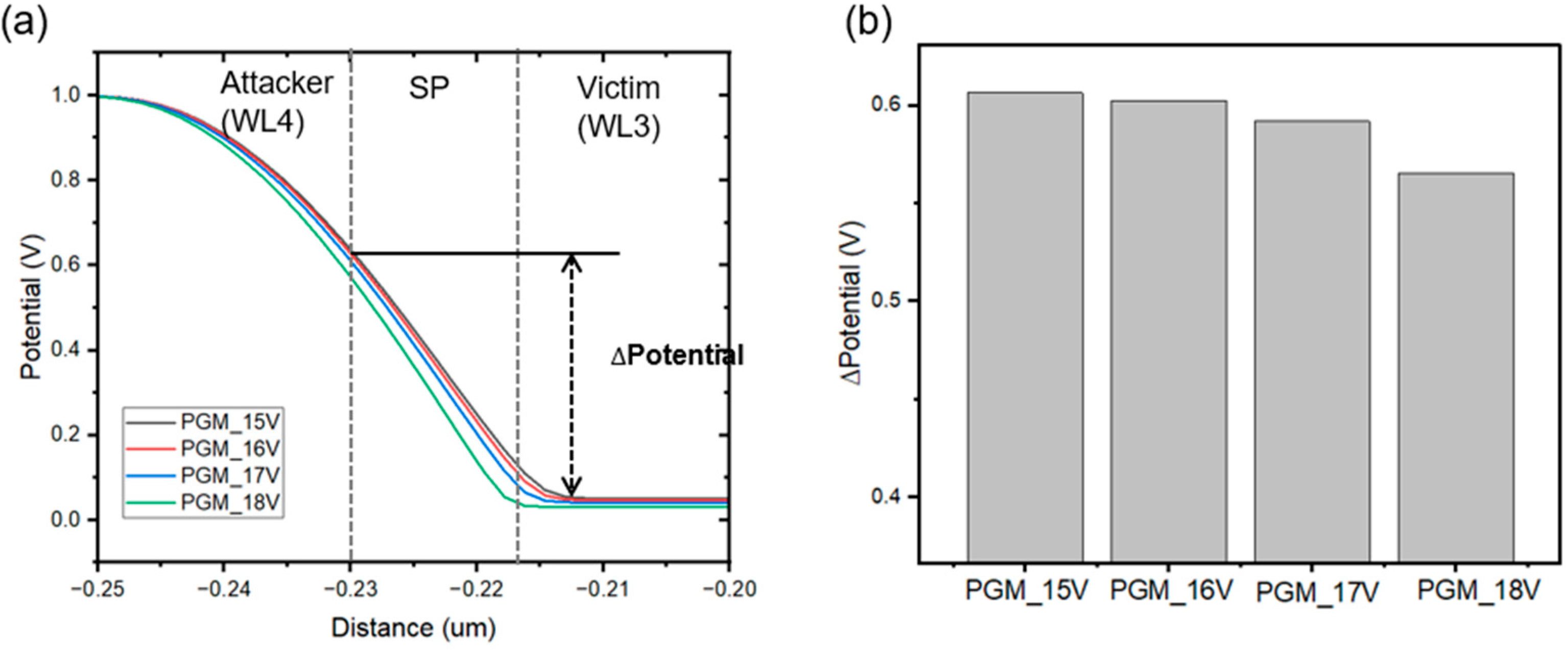
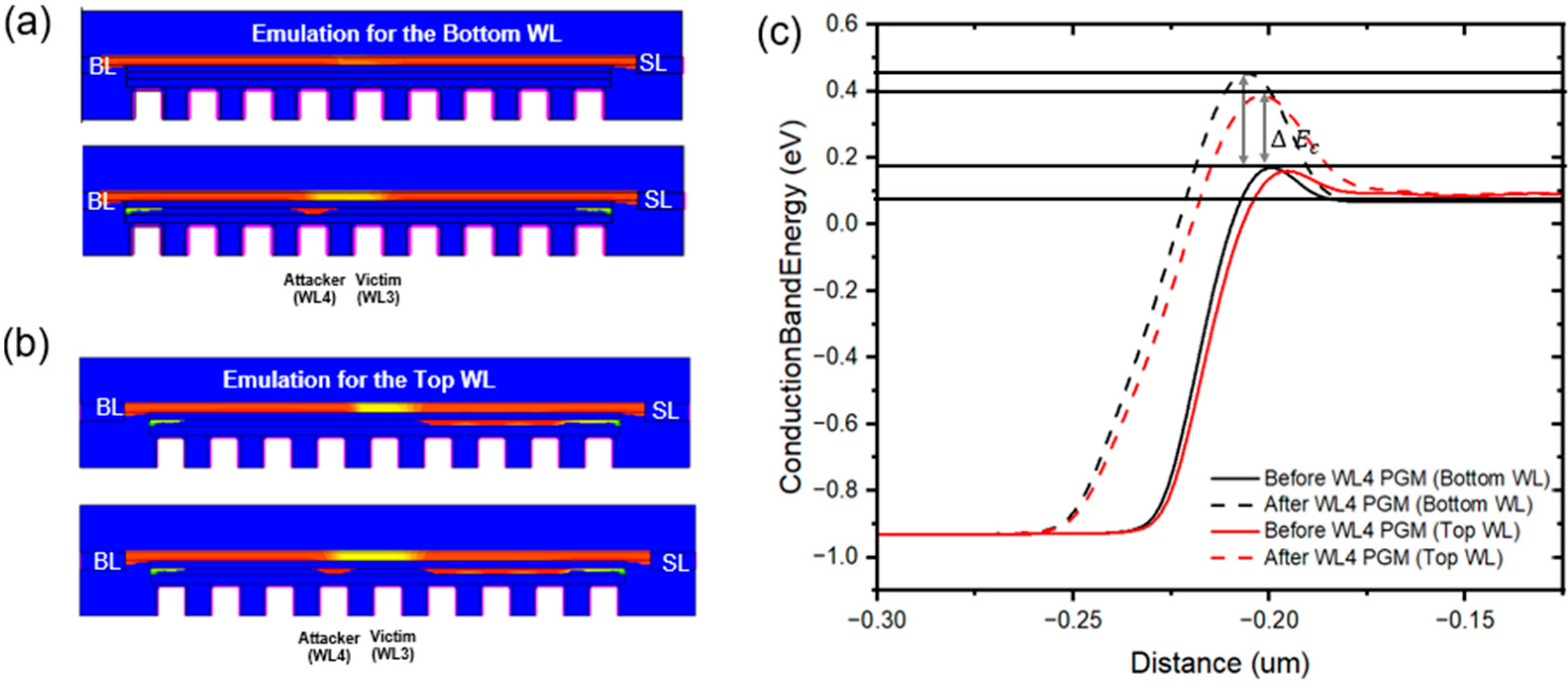
3. Asymmetric Z-Interference Analysis

To analyze the results depicted in Figure 1a, we constructed TCAD simulations for two programming sequences: from the Top WL to the Bottom WL and from the Bottom WL to the Top WL. Figure 2a illustrates the programming environments at the bottom WL and Top WL, respectively, for the sequence from the Bottom WL to the Top WL. When programming from bottom to top, the Bottom WL is the first WL to be programmed within the entire string. [8]. To simulate this Bottom WL environment, we applied a small amount of programming to WLs 0, 1, and 2, assuming no WLs are stored in the CTN layer of the string. Conversely, when programming from bottom to top and focusing on the Top WL, most of the lower WLs, excluding the Top WL, have completed their programming operations. Therefore, to simulate programming environments for the Bottom, Middle, and Top WLs, we increased the programming levels for WLs 0, 1, and 2 with respect to the selected WL (WL3). Similarly, for programming from the Top WL to Bottom WL in Figure 2b, we adjusted electron trapped charge levels for WL4, WL5, and WL6 to replicate top/middle/bottom programming environments. Subsequently, in both sequences, Bottom WL to Top WL and Top WL to Bottom WL, WL3 was designated as the victim cell, with WL2 and WL4 sequentially programmed by applying 17 V as attack cells. The degree of Z-interference was calculated based on the initial Vth of WL3 and the subsequent Vth shift after programming the attack cell. Through simulations, we obtained results similar to previous studies, as shown in Figure 2c, confirming the successful execution of the simulations. Figure 2c also demonstrates, consistent with prior research, that programming from Top WL to Bottom WL mitigates Z-interference more effectively than programming from the Bottom WL to the Top WL. This is attributed to inherent asymmetrical interference patterns based on the positions of the programmed neighboring cells. Unlike 2D NAND flash memory, where the CTN layer is not distributed across the entire string, 3D NAND flash memory places the CTN layer throughout the entire string. As a result, the fringing field generated during programming can cause both electrons and holes to be programmed into the adjacent spacer regions between the attack cell and the victim cell. These programmed charges affect the electron concentration in the Poly-Si channel, becoming a major cause of Z-interference [9]. Additionally, Z-interference can vary depending on the positions of adjacent cells. If the attack cell is located towards the drain side, Z-interference is accelerated compared to when it is towards the source side, due to the Drain Induced Barrier Lowering (DIBL) effect. This asymmetry arises due to DIBL effects, where during read operations in 3D NAND flash, gate biases of WLs excluding the Victim WL are applied as read voltages. Consequently, all bit-line voltages are applied only to the Victim WL, leading to the occurrence of DIBL effects in the Victim WL [10]. The programming method from the Bottom WL to the Top WL, as depicted in Figure 2a, significantly impacts DIBL effects because the attack WL is oriented in the bit-line direction. Conversely, the programming method from Top WL to Bottom WL, as shown in Figure 2b, minimizes the influence of DIBL effects since the Attack WL is oriented in the source-line direction. Therefore, the programming sequence from Top WL to Bottom WL results in fewer Z-interference effects [1,11].
We conducted an in-depth analysis of the sequence from the Bottom WL to Top WL program. Figure 2c demonstrates a gradual reduction in Z-interference as programming progresses from the Bottom to Top WLs. This reduction occurs because the poly-Si channel load resistance increases gradually as more programming is applied to the Bottom WLs [12], as illustrated in Figure 3a,b. In these figures, we compared the potential differences observed in the channel of the victim cell during read operations with WLs programmed from WL0 to WL2 at voltages ranging from 15 V to 18 V. Because the channel resistance under the WLs of the Attacker and Victim cells is relatively much higher than the channel resistance under other WLs, most of the voltage appears across the Attacker and Victim cells. We programmed the attack cell at a consistent 17 V and observed a decrease in channel potential near the victim cell, more pronounced when the WL near the source was programmed at 18 V compared to 15 V [13]. When WL0 to WL2 is programmed at 18 V, the amount of trapped charge generated near the Bottom WL increases compared to programming at 15 V, leading to an increase in the resistance of the poly-Si channel of the Bottom WL. As a result, more bitline voltage is applied to the poly-Si channel area of the Bottom WL, causing a lower potential to be applied to the victim cell and reducing the DIBL effect caused by the attack cell. Therefore, assuming 15 V programming as bottom programming and 18 V programming as top programming, the cause of the WL-related Z interference changes shown in Figure 1a can be understood. To further analyze the impact of the channel resistance near the programmed Bottom WL, Figure 4a,b were compared. Figure 4a represents a scenario without resistance near the source, simulating the situation during Bottom WL programming. Figure 4b illustrates the situation during Top WL programming. In both cases, the conduction band profiles of the victim cell due to the attack cell during read operations were investigated in Figure 4c. During the read operation, a fixed voltage near Vth was applied to the victim cell, while the remaining cells were subjected to a uniform voltage of 7 V. As expected, there is less change in the source-to-gate barrier in the Top WL programming situation compared to the Bottom WL programming situation, indicating a lesser impact on the poly-Si channel conduction due to the attack cell programming. Programming at Top WL results in less voltage applied to the victim cell when the same bit-line voltage is applied due to the influence of the channel resistance of the cells already programmed at the Bottom WL. Therefore, adjusting the bitline voltage appropriately by considering the degree of channel resistance within the string when programming the selected WLs can be considered a method to improve the Vth variation due to Z-interference.

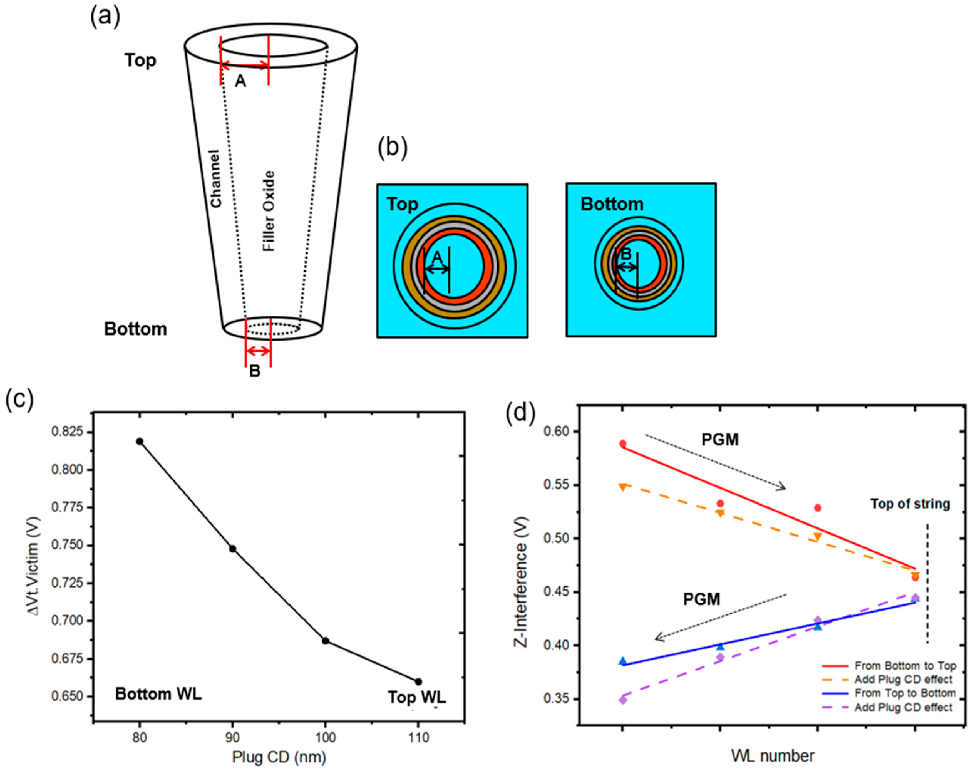
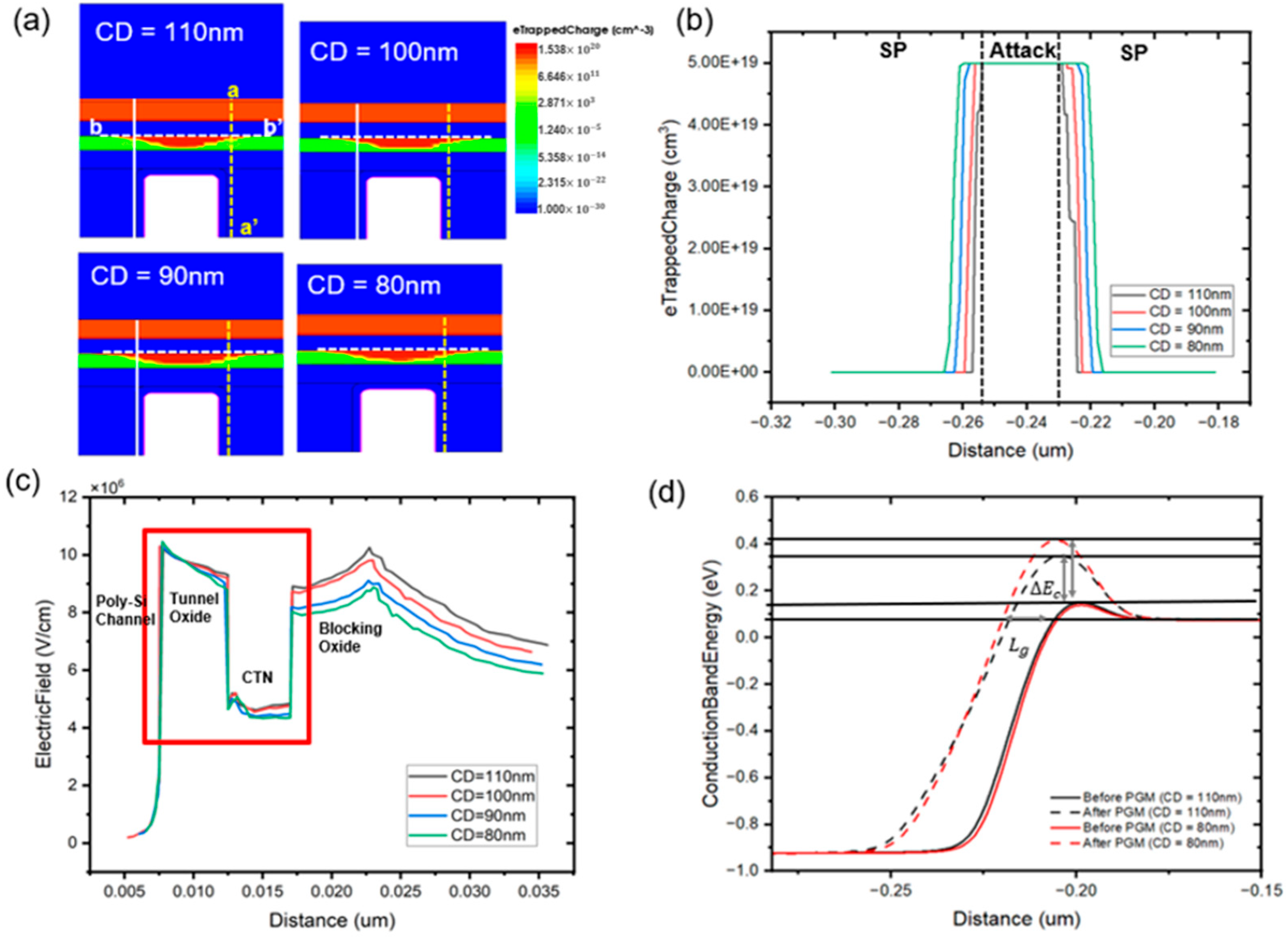
4. Effects of Tapered Shape of the Channel Hole

Figure 1a and Figure 2c show similar trends in Z-interference changes according to the programming sequence. However, a detailed look at the actual measurements in Figure 1a reveals that the Z-interference change is greater when programming from the Bottom WL to the Top WL compared to programming from the Top WL to the Bottom WL. This result differs from the findings in Figure 2c. To further analyze the causes of this discrepancy, we incorporated the actual 3D NAND flash stack structure. Three-dimensional NAND employs XYZ scaling to achieve higher memory density. XY scaling reduces cell spacing, and Z scaling adds more layers, often with layer pitch reduction (Z reduction) to minimize physical height increase. Z-stacking has been a prominent approach for achieving high memory density [14]. However, as demand for higher memory density increases, the number of layers also increases, posing new technological challenges due to process limits. The method of forming cell stacks in 3D NAND involves etching holes through oxide/nitride stacks, followed by deposition of gate oxide and channel [15]. Therefore, 3D NAND forms cylindrical channels within the holes and is commonly referred to as Gate-All-Around (GAA) due to gates surrounding the channel. However, as the number of layers increases, the aspect ratio of the channel increases, making etching processes more challenging. Consequently, the taper angle leads to asymmetrical characteristics between upper and lower cells. In GAA 3D NAND structure, such non-ideal vertical etching significantly induces inter-layer variations, particularly sensitive to curvature-induced field enhancement. Refs. [16,17] Figure 5a illustrates the structure of the taper angle due to process variation. Figure 5b shows the difference in channel diameter between the top and bottom cells due to the taper angle. To apply these varying diameters of Top WL and Bottom WL, we performed simulations by adjusting the Plug CD size for each WL. Figure 5c demonstrates that as Plug CD decreases, the Z-interference of the victim cell increases. In other words, the Z-interference increases more rapidly in the Bottom WL than in the Top WL. Based on these results, we re-analyzed Z-interference in Figure 2c. As shown in Figure 5d, when different channel diameters are applied to the Top WL and Bottom WL, the amount of Z-interference change for the WL resistance change is larger when evaluating the Bottom WL to Top WL program compared to the Top WL to Bottom WL program. These results align well with the actual measurement trends observed in Figure 1a.
The difference in channel diameter between the upper and lower WL, resulting from the taper angle, affects the electrical characteristics of the flash memory. To analyze this, we varied the Plug CD size from 80 nm to 110 nm and compared the amount of trapped electrons in the charge trap layer during the programming operation. Figure 6a shows that as the Plug CD increases, the distribution of programmed electrons in the spacer region becomes wider [18]. Figure 6b is a graph quantitatively comparing the electron concentration along the b-b′ cut line from Figure 6a. To further analyze this phenomenon, the changes in electric field and conduction band with respect to the Plug CD size are investigated in Figure 6c,d. Figure 6c shows the electric field profile along the a-a′ cut line from Figure 6a. It demonstrates that when the CD is smallest at 80 nm, the electric field across the tunnel oxide is the highest. Generally, the smaller the Plug CD, the more electric field is generated in the tunnel oxide due to Gauss’s law [19]. Consequently, as the channel diameter decreases, the charge density in the spacer region increases after programming the attack cell, having a greater impact on the Z-interference of the victim cell. Figure 6d shows the changes in the conduction band observed in the victim cell when there is an identical programmed Vth change in the attack cell. During the read operation, a fixed voltage close to the threshold voltage was applied to the victim cell before and after programming the attack cell, while 7 V was applied to the other cells. Consistent with earlier results, a more pronounced change in conduction band energy was observed when the Plug CD was 80 nm compared to 110 nm. Additionally, defining the effective gate length of the victim cell as the distance between the energy level at the source line point and the bitline direction, it was found that the effective gate length increases significantly as the channel diameter decreases. Therefore, to achieve consistent Z-interference changes across the programmed WL, it is crucial to minimize process and structural differences in WL cells [20]. Especially as Z-interference degradation increases sharply with ON (Oxide/Nitride) Mold Pitch [21] Pitch, which refers to the One WL stack height in 3D NAND, it is necessary to improve Vth distribution across the entire string through the HARC (high aspect ratio contact) etching process [22].

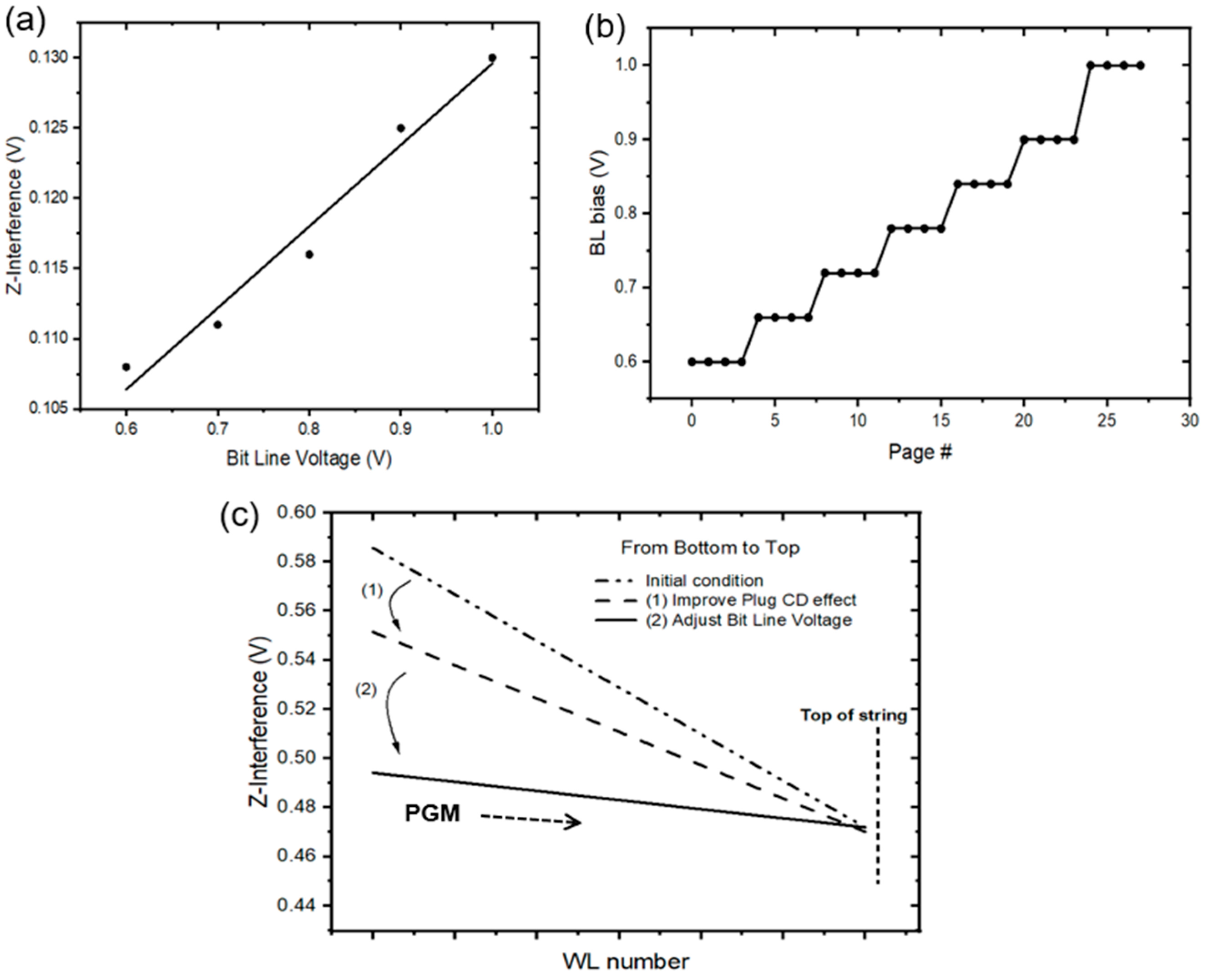
5. Improving Z-Interference by Adjusting Bitline Voltage

As analyzed in Figure 5d, the degree of channel resistance within the string during the programming of the selected WL induces significant changes in Z-interference. Considering this variability in advance and appropriately adjusting the BL voltage for each WL during programming could be a promising development direction to further enhance WL-specific Z-interference variability. Figure 7a shows the changes in Z-interference according to the BL voltage during the verification operation of the selected WL when programming the Bottom WL. It demonstrates that as the BL voltage decreases, Z-interference decreases when reading the victim WL after programming the attack cell. This is because the reduction in BL voltage causes a decrease in the DIBL effect.
Based on these results, Figure 7b proposes a method of applying variable BL voltages for each WL. By maintaining a consistent and effective BL voltage applied to the victim WL according to the channel resistance of the previously programmed WL, Z-interference changes can be greatly improved. Specifically, cells programmed earlier have lower channel resistance, and, therefore, a lower BL voltage is applied. Conversely, cells programmed later have higher channel resistance during the verification operation, so a higher BL voltage is applied. Reducing the BL voltage can potentially lead to incorrect verification results due to decreased cell current. However, in the proposed method for verifying the Bottom WL, lowering the BL voltage to 40% or less does not result in incorrect verification. Typically, when programming from the Bottom to Top WLs, the BL voltage used in a 3D NAND string is selected to ensure sufficient current during the verification of the Top WL. This means that, during the verification of the Bottom WL, the BL voltage is set to provide more than twice the minimum current required, even though no WLs in the string are programmed.
Therefore, setting the BL voltage for Bottom WL verification to 50% or less of the reference BL voltage used for the Top WL ensures that the verification process is not adversely affected. By designing and implementing the WL-specific BL bias modulation scheme proposed in this paper, we can significantly improve WL-specific Z-interference, as demonstrated in Figure 7c.

6. Conclusions

This study presents a comprehensive analysis of Z-interference in 3D NAND flash memory, focusing on the impact of programming sequences and vertical channel tapering. The phenomenon of Z-interference varies significantly depending on the programming environment of Bottom WL and Top WL in 3D NAND flash. Particularly, in the programming situation from the bottom to the top, we observed that during the programming of the Bottom WL, the channel resistance at the bottom decreases, enhancing the Drain Induced Barrier Lowering (DIBL) effect due to the bitline voltage. Simultaneously, we confirmed the tapered vertical channel structure, where the reduction in channel diameter near Bottom WL intensifies the electric field compared to Top WL, exacerbating Z-interference phenomena. Therefore, we propose a method to uniformly adjust the channel diameter distribution and appropriately regulate bitline biases during read operations of each WL. These findings contribute to the development of more reliable and high-performance 3D NAND flash memory devices, offering valuable insights for future technological advancements in the field.

Author Contributions

Conceptualization, J.K.P.; methodology, J.K.P.; software, Y.J.C.; validation, S.K.H.; formal analysis, Y.J.C. and S.K.H.; investigation, Y.J.C.; writing—original draft preparation, Y.J.C.; writing—review and editing, J.K.P.; visualization, Y.J.C.; supervision, J.K.P.; project administration, J.K.P.; funding acquisition, J.K.P. All authors have read and agreed to the published version of the manuscript.

Funding

This study was supported by the research program funded by SeoulTech (Seoul National University of Science and Technology).

Data Availability Statement

Data are contained within the article.

Conflicts of Interest

The funders had no role in the design of the study; in the collection, analyses, or interpretation of data; in the writing of the manuscript; or in the decision to publish the results.

References

  1. Heineck, L.; Liu, J. 3D NAND flash status and trends. In Proceedings of the 2022 IEEE International Memory Workshop (IMW), Dresden, Germany, 15–18 May 2022; pp. 1–4. [Google Scholar]
  2. Goda, A. 3-D NAND technology achievements and future scaling perspectives. IEEE Trans. Electron Devices 2020, 67, 1373–1381. [Google Scholar] [CrossRef]
  3. Chandrasekaran, N.; Ramaswamy, N.; Mouli, C. Memory technology: Innovations needed for continued technology scaling and enabling advanced computing systems. In Proceedings of the 2020 IEEE International Electron Devices Meeting (IEDM), San Francisco, CA, USA, 12–18 December 2020. [Google Scholar]
  4. Yang, L.; Wang, Q.; Li, Q.; Yu, X.; He, J.; Huo, Z. Efficient data recovery technique for 3D TLC NAND flash memory based on WL interference. In Proceedings of the 2021 IEEE International Reliability Physics Symposium (IRPS), Monterey, CA, USA, 21–25 March 2021. [Google Scholar]
  5. Liu, W.; Wu, F.; Chen, X.; Zhang, M.; Wang, Y.; Lu, X.; Xie, C. Characterization summary of performance, reliability, and threshold voltage distribution of 3D charge-trap NAND flash memory. ACM Trans. Storage (TOS) 2022, 18, 1–25. [Google Scholar] [CrossRef]
  6. Chang, Y.-W.; Wu, G.-W.; Yang, I.-C.; Huang, Y.-H.; Lee, Y.-J.; Lee, C.-H.; Chen, K.-F.; Lu, T.-C.; Chen, K.-C.; Lu, C.-Y. Asymmetric interference behavior in 3D NAND cell and the reverse trend induced by undercut of sacrificial nitride film. IEEE Electron Device Lett. 2022, 43, 2077–2080. [Google Scholar] [CrossRef]
  7. Kim, Y.; Hong, S.K.; Park, J.K. Optimizing Confined Nitride Trap Layers for Improved Z-Interference in 3D NAND Flash Memory. Electronics 2024, 13, 1020. [Google Scholar] [CrossRef]
  8. Chen, W.-C.; Lue, H.-T.; Hsieh, C.-C.; Wang, K.-C.; Lu, C.-Y. Performance enhancement of 3-D NAND flash featuring a two-step dummy wordline program waveform and pair-bitline program scheme. IEEE Trans. Electron Devices 2019, 67, 99–104. [Google Scholar] [CrossRef]
  9. Sim, J.-M.; Kang, M.; Song, Y.-H. A new read scheme for alleviating cell-to-cell interference in scaled-down 3D NAND flash memory. Electronics 2020, 9, 1775. [Google Scholar] [CrossRef]
  10. Yi, S.-i.; Kim, J. Novel program scheme of vertical NAND flash memory for reduction of Z-interference. Micromachines 2021, 12, 584. [Google Scholar] [CrossRef] [PubMed]
  11. Jo, H.; Ahn, S.; Shin, H. Investigation and modeling of Z-interference in poly-Si channel-based 3-D NAND flash memories. IEEE Trans. Electron Devices 2022, 69, 543–548. [Google Scholar] [CrossRef]
  12. Chen, W.-C.; Lue, H.-T.; Chang, K.-P.; Hsiao, Y.-H.; Hsieh, C.-C.; Shih, Y.-H.; Lu, C.-Y. Study of the programming sequence induced back-pattern effect in split-page 3D vertical-gate (VG) NAND flash. In Proceedings of the Technical Program—2014 International Symposium on VLSI Technology, Systems and Application (VLSI-TSA), Hsinchu, Taiwan, 28–30 April 2014; pp. 1–2. [Google Scholar]
  13. Fan, H.; Tian, X.; Peng, H.; Shen, Y.; Li, L.; Li, M.; Gao, L. Adaptive Bitline Voltage Countermeasure for Neighbor Wordline Interference in 3D NAND Flash Memory-Based Sensors. Sensors 2023, 23, 3212. [Google Scholar] [CrossRef] [PubMed]
  14. Goda, A. Recent progress on 3D NAND flash technologies. Electronics 2021, 10, 3156. [Google Scholar] [CrossRef]
  15. Lee, D.; Shin, C. Impact of Stacking-Up and Scaling-Down Bit Cells in 3D NAND on Their Threshold Voltages. Micromachines 2022, 13, 1139. [Google Scholar] [CrossRef] [PubMed]
  16. Wu, C.-J.; Lue, H.-T.; Hsu, T.-H.; Hsieh, C.-C.; Chen, W.-C.; Du, P.-Y.; Chiu, C.-J.; Lu, C.-Y. Device characteristics of single-gate vertical channel (SGVC) 3D NAND flash architecture. In Proceedings of the 2016 IEEE 8th International Memory Workshop (IMW), Paris, France, 15–18 May 2016. [Google Scholar]
  17. Yoon, D.; Sim, J.; Song, Y. Mechanical stress in a tapered channel hole of 3D NAND flash memory. Microelectron. Reliab. 2023, 143, 114941. [Google Scholar] [CrossRef]
  18. Lee, J.G.; Jung, W.J.; Park, J.H.; Yoo, K.-H.; Kim, T.W. Effect of the blocking oxide layer with asymmetric taper angles in 3-D NAND flash memories. IEEE J. Electron Devices Soc. 2021, 9, 774–777. [Google Scholar] [CrossRef]
  19. Kim, S.S.; Yong, S.K.; Kim, W.; Kang, S.; Park, H.W.; Yoon, K.J.; Sheen, D.S.; Lee, S.; Hwang, C.S. Review of semiconductor flash memory devices for material and process issues. Adv. Mater. 2023, 35, 2200659. [Google Scholar] [CrossRef] [PubMed]
  20. Bhatt, U.M.; Manhas, S.K.; Kumar, A.; Pakala, M.; Yieh, E. Mitigating the impact of channel tapering in vertical channel 3-D NAND. IEEE Trans. Electron Devices 2020, 67, 929–936. [Google Scholar] [CrossRef]
  21. Yoon, C.-W. The Fundamentals of NAND Flash Memory: Technology for tomorrow’s fourth industrial revolution. IEEE Solid-State Circuits Mag. 2022, 14, 56–65. [Google Scholar] [CrossRef]
  22. Shim, S.I.; Jang, J.; Song, J. Trends and future challenges of 3D NAND flash memory. In Proceedings of the 2023 IEEE International Memory Workshop (IMW), Monterey, CA, USA, 21–24 May 2023. [Google Scholar]
Figure 1. (a) Z-interference differences of each WL in state PV1 (Program Verify Level) after subsequent WL programming, using two programming schemes with opposite sequences. Reprinted/adapted with permission from Ref. [6] 2022, IEEE. (b) A schematic cross-section of the 3D NAND string used in the simulation. (c) Detailed zoom-in view of (b) and the corresponding simulated parameters.
Electronics 13 03123 g001
Figure 2. Simulation structure according to the program sequence. (a) Program sequence from the Bottom WL to the Top WL. (b) Program sequence from the Top WL to the Bottom WL. (c) Z-interference simulation results for (a,b).
Electronics 13 03123 g002
Figure 3. (a) Poly-Si channel potential results applied to the victim cell during read operation after Bottom WL (WL0 to WL2) programming. (b) Comparison of potential differences in (a).
Electronics 13 03123 g003
Figure 4. (a) Structure simulating the Bottom WL programming situation. (b) Structure simulating the Top WL programming situation. (c) Comparison of conduction band energy before and after the attack cell programming in situations (a,b).
Electronics 13 03123 g004
Figure 5. (a) The structure of taper angle variations in 3D NAND flash. (b) difference in channel diameters between Top Word Line (WL) and Bottom WL. (c) Z-interference simulation results as a function of Plug CD size. (d) simulation results demonstrating changed Z-interference when different channel diameters are applied to the Top WL and Bottom WL.
Electronics 13 03123 g005
Figure 6. (a) Electron trapped charge profiles in the charge trap nitride after programming, according to different Plug CD sizes. (b) Electron trapped charge observed along the b-b′ cut line in (a). (c) Electric field profile results observed along the a-a′ cut line in (a). (d) Comparison of conduction band energy before and after programming the attack cell, with Plug CD sizes of 80 nm and 110 nm.
Electronics 13 03123 g006
Figure 7. (a) Z-interference results according to BL voltage during the verification operation in the Bottom WL programming situation. (b) Example of variable BL voltage operation scheme during the programming operation from the Bottom WL to the Top WL. Depiction of a case where one block consists of four strings. (c) Results of improved Z-interference by applying selective BL voltage scheme from the Bottom WL to the Top WL.
Electronics 13 03123 g007
Table 1. Simulation voltage conditions.
ProgramEraseRead
Selected cell15 V~18 V0 V−6 V~5 V
Unselected cell8.5 V0 V7 V
BL0 V22 V1 V
DSL8.5 VFloating7 V
SSL0 VFloating7 V
SL2 V22 V0 V
Disclaimer/Publisher’s Note: The statements, opinions and data contained in all publications are solely those of the individual author(s) and contributor(s) and not of MDPI and/or the editor(s). MDPI and/or the editor(s) disclaim responsibility for any injury to people or property resulting from any ideas, methods, instructions or products referred to in the content.

