Communication

Study on the Single-Event Burnout Effect Mechanism of SiC MOSFETs Induced by Heavy Ions

Department of Nuclear Physics, China Institute of Atomic Energy, Beijing 102413, China
*
Author to whom correspondence should be addressed.
Electronics 2024, 13(17), 3402; https://doi.org/10.3390/electronics13173402
Submission received: 26 July 2024 / Revised: 17 August 2024 / Accepted: 20 August 2024 / Published: 27 August 2024

Abstract

:
As a prominent focus in high-voltage power devices, SiC MOSFETs have broad application prospects in the aerospace field. Due to the unique characteristics of the space radiation environment, the reliability of SiC MOSFETs concerning single-event effects (SEEs) has garnered widespread attention. In this study, we employed accelerator-heavy ion irradiation experiments to study the degradation characteristics for SEEs of 1.2 kV SiC MOSFETs under different bias voltages and temperature conditions. The experimental results indicate that when the drain-source voltage (VDS) exceeds 300 V, the device leakage current increases sharply, and even single-event burnout (SEB) occurs. Furthermore, a negative gate bias (VGS) can make SEB more likely via gate damage and Poole–Frenkel emission (PF), reducing the VDS threshold of the device. The radiation degradation behavior of SiC MOSFETs at different temperatures was compared and analyzed, showing that although high temperatures can increase the safe operating voltage of VDS, they can also cause more severe latent gate damage. Through an in-depth analysis of the experimental data, the physical mechanism by which heavy ion irradiation causes gate leakage in SiC MOSFETs was explored. These research findings provide an essential basis for the reliable design of SiC MOSFETs in aerospace applications.

1. Introduction

SiC MOSFETs exhibit outstanding advantages, such as high operating voltage, low power consumption, and high operating temperature, making them high-voltage power devices of significant interest in the aerospace field [1,2,3]. In response to the application requirements of the space radiation environment, both domestic and international researchers have investigated the effects of radiation on SiC MOSFETs, including total dose effects, SEEs, and displacement damage effects [4,5,6]. Studies have shown that SEEs, particularly SEBs, caused by cosmic rays and particles, seriously threaten the reliability of SiC MOSFETs. Robert et al. [7] found that when the incident particle linear energy transfer (LET) is greater than 10 MeV·cm2/mg and the bias voltage is 100 V, irreversible leakage current degradation can occur, and that at 400 V, the device will suffer SEB damage. They also noted [8] that the impact of the leakage current should be evaluated based on the application conditions of the device. Martinella et al. [4,5,9] found that the permanent damage caused by ions to the internal structures of SiC MOSFETs leads to a decrease in leakage current and breakdown voltage, which is directly related to the LET of the incident particles and the drain-source bias voltage. Witulski et al. [10,11] discovered that under the influence of an electric field, the electron–hole pairs generated by heavy ion ionization accumulate, causing the local temperature to reach 3600 K, surpassing the melting point of SiC and resulting in lattice damage, thereby causing SEB. In contrast, leakage current degradation is caused by the eutectic state of the SiC and the metal, without complete lattice structure damage. Combining domestic and international research progress, it is known that the radiation effect degradation performances and mechanisms of SiC MOSFETs differ from those of traditional Si-based devices. Research on the radiation effects of SiC MOSFETs is highly important for promoting their reliable space application.
This paper focuses on the 1.2-kilovolt SiC MOSFET by conducting accelerator heavy ion irradiation experiments to study the SEEs. The degradation performance of SiC MOSFETs under different bias voltages and temperature conditions was analyzed, and the physical mechanism of heavy ion irradiation leading to gate leakage was explored. This research provides a foundation for the reliable application of SiC MOSFETs.

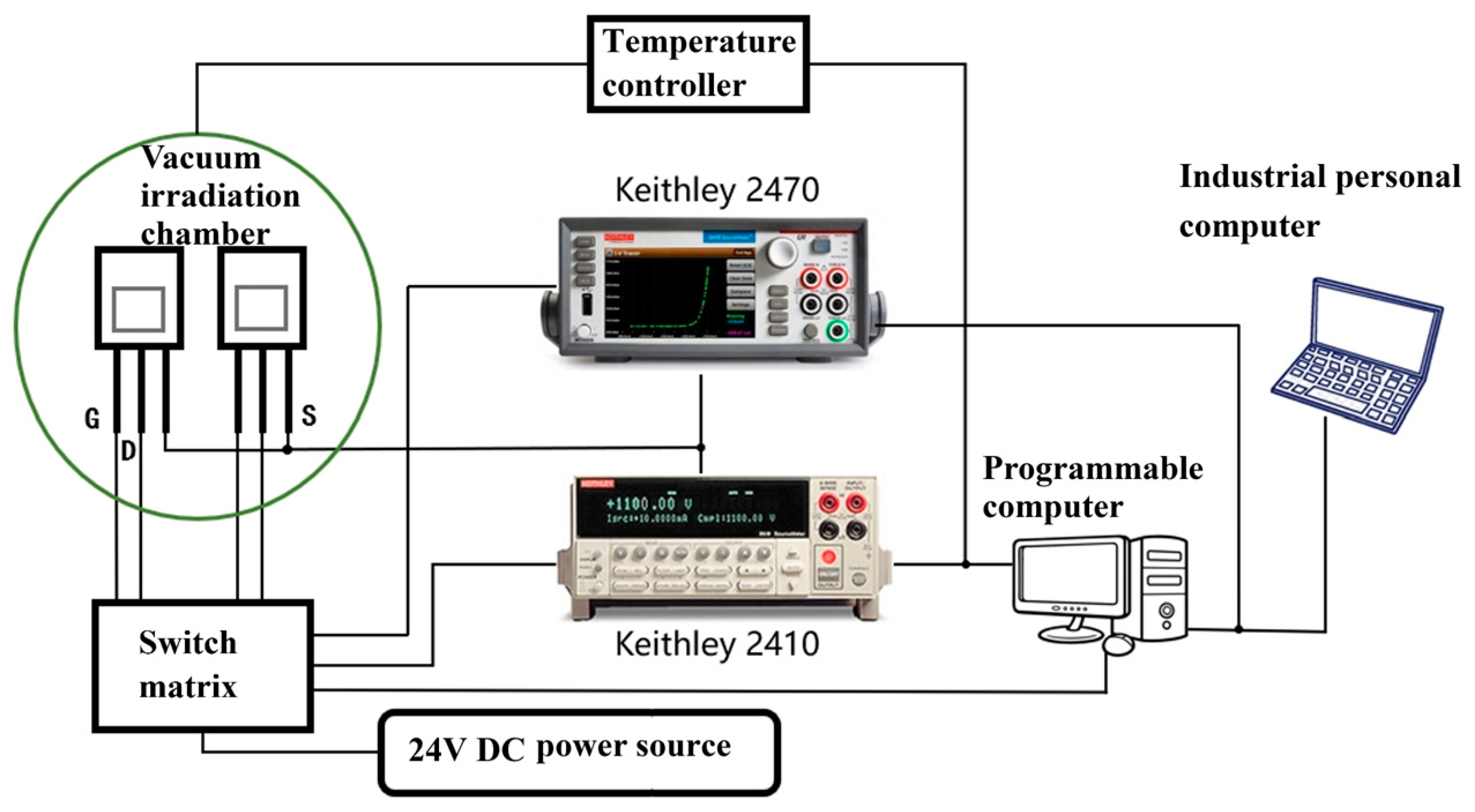
2. Experimental Setup

The experimental samples used were fourth-generation symmetric trench gate SiC MOSFETs from Rohm (Kyoto, Japan), with an average operating voltage of 1.2 kV, packaged in TO-247-4 L. The heavy ion irradiation experiment was conducted using an HI-13 tandem accelerator in Beijing. The heavy ions chosen for irradiation were 138 MeV Cl particles, with LET of 14.63 MeV·cm2·mg−1 and range of 26.11 μm in SiC. Before irradiation, all the samples were decapped and dies in them were exposed. Two samples were irradiated under each experimental condition, and a switch matrix was used to determine the power on and current monitoring of irradiated devices.
A block representation of the experimental setup (shown in Figure 1) was constructed to monitor the drain-source and gate-source currents of the irradiated device in real time. Two Keithley source measure units (SMUs), models 2470 and 2410, were used to bias gate (VGS) and drain (VDS), respectively. Furthermore, model 2410 was used to monitor the drain currents (ID). The gate and drain were connected to the positive poles of the two source meters, and the source was connected to the negative poles of the two source meters simultaneously to monitor the two currents separately. The source meters were remotely controlled by a host computer for program control and data storage. Before the beam was turned on, the gate and source of the SiC MOSFET were short-circuited, i.e., VGS = 0 V and VDS = 100 V. After irradiation started, the process stopped when the total amount of incident ions reached 1 × 10⁶ cm−2. Next, the irradiation continued after increasing the VDS until the drain-source current exceeded 1 × 10⁻⁴ A, indicating the occurrence of SEB, and the irradiation experiment ended.

3. Results and Discussion

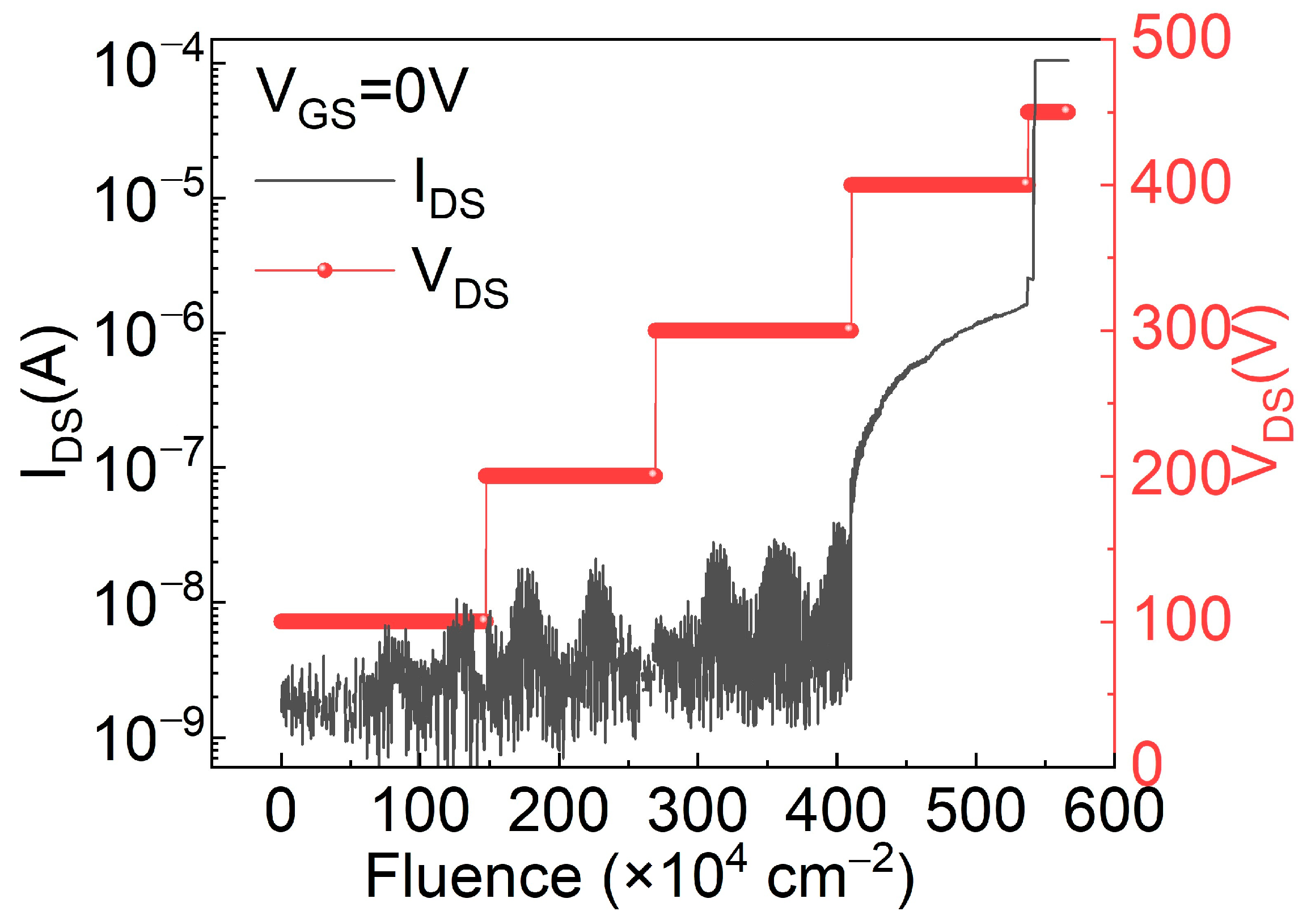
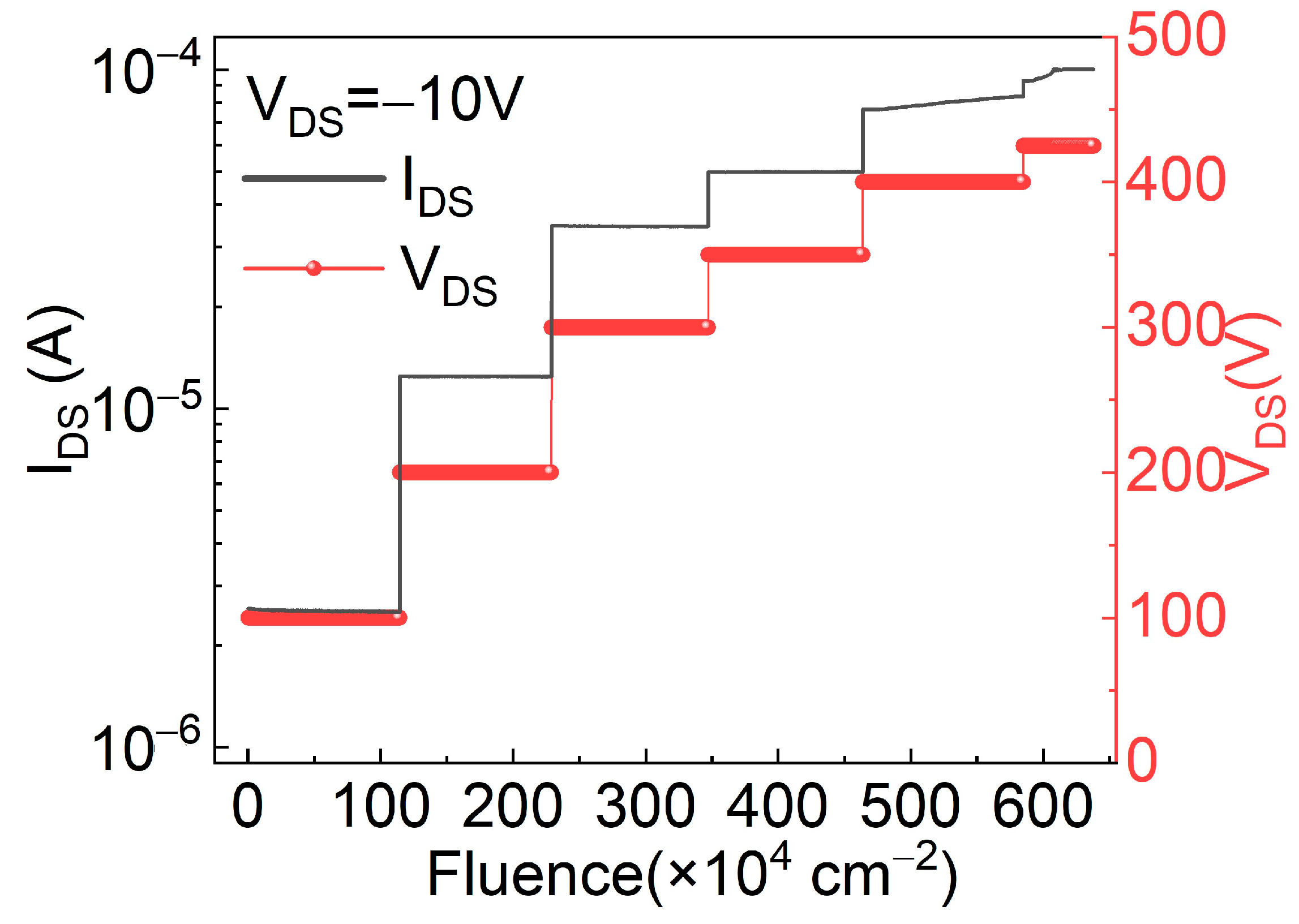
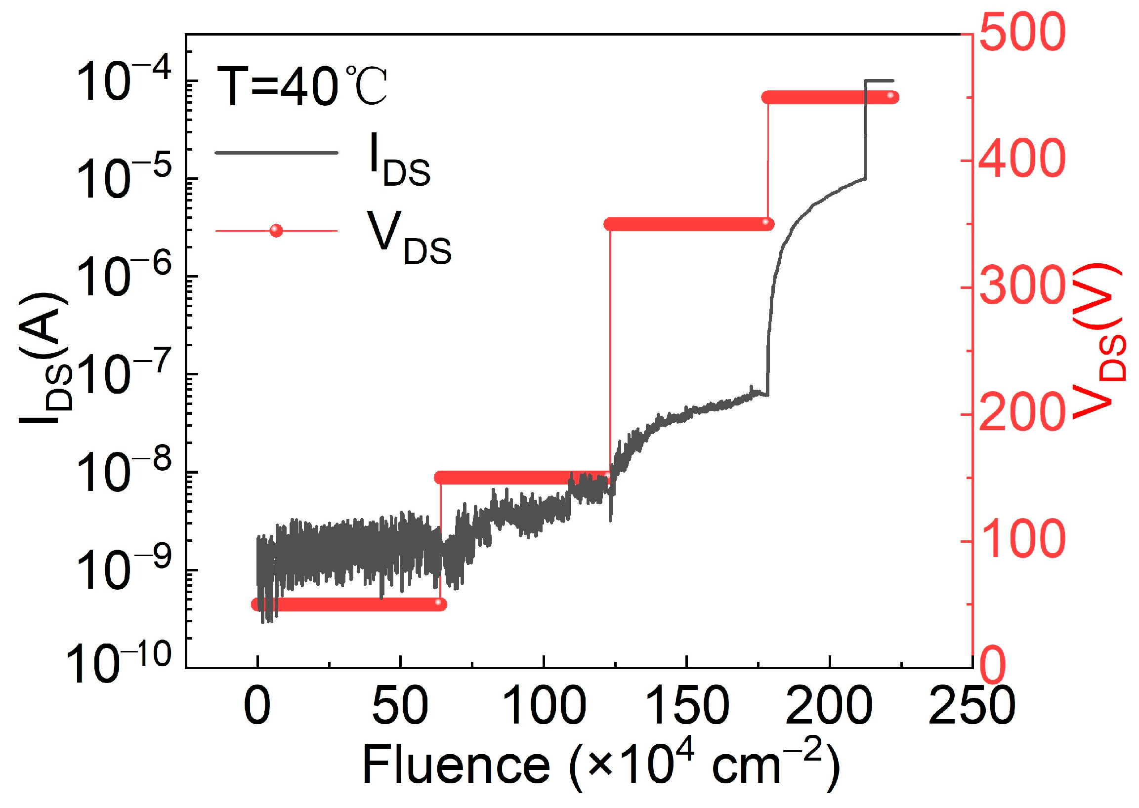
3.1. Degradation Characteristics of SiC MOSFET under Heavy Ion Irradiation

Figure 2 shows the changes in the gate current, drain current, and VDS of the SiC MOSFETs with respect to the irradiation time during the heavy ion irradiation experiment. The heavy ion injection rate in this round of experiments was 1.18 × 104 cm−2·s−1. As shown in the figure, when VDS < 300 V, the drain current of the device remains small and relatively stable, with minimal changes in VDS. Above VDS = 400 V, the drain current rapidly increases by three orders of magnitude, and when the voltage reaches VDS = 450 V, the drain current instantly spikes, leading to SEB.
The effect of the gate-source bias voltage VGS on device SEB degradation was studied. In this round of experiments, the devices were placed in an off state, VGS = −10 V, and the heavy ion injection rate was 1.16 × 104 cm−2·s−1. The curves of the gate current, drain current, and VDS of the SiC MOSFET with respect to the irradiation time during the heavy ion irradiation experiment are shown in Figure 3. When VDS = 100 V, the drain current increases significantly compared with that at VGS = −10 V, as shown in Figure 2, and the drain current shows great stability under different VDS levels. Until VDS = 400 V, the drain current gradually increases with the injection rate of the irradiated particles, and drain current degradation occurs, but SEB does not occur. Finally, when VDS = 425 V, the current change slope increases. Under these conditions, the cumulative irradiation time is approximately 20 s, and SEB occurs when the current reaches the preset threshold. It can be concluded that when VGS = −10 V and VDS < 350 V, the SiC MOSFET has no sensitive response to radiation injection and can maintain a relatively stable working state.
The experiment was conducted again with the gate-source bias changed. Figure 4 shows the drain current and VDS values of the SiC MOSFET with respect to the fluence with VGS = −15 V. In this case, the heavy ion injection rate was 1.15 × 104 cm−2·s−1. As shown in the figure, when VDS = 400 V, the drain current began to increase with increasing incident injection, and SEB occurred after approximately 20 s of cumulative irradiation under these conditions. Similarly, when the initial VDS voltage was 100 V, the drain current was maintained at a high level, and the drain current was stable under different bias conditions. Figure 4 shows that the sample can maintain a relatively stable working state when VGS = −15 V and VDS < 375 V, and that it will not respond sensitively to irradiation.
Comparing the SEBs of the samples under three gate-source bias conditions, Figure 2, Figure 3 and Figure 4 show that the SEB threshold voltage decreases with increases in the absolute value of the negative bias of the gate-source voltage. This is because different gate-source biases cause different degrees of damage to the internal oxide layer of the SiC MOSFET [12]. A post-irradiation gate stress (PIGS) test was carried out to explore the relationship between the potential damage to the gate oxide and the gate-source bias voltage VGS during the irradiation, and the results are shown in Figure 5. After irradiation with VGS = 0 V, the gate leakage current IGS had no obvious change; after irradiation with VGS = −10 V, the device IGS was one order of magnitude larger than that before irradiation; after irradiation with VGS = −15 V, the IGS changed significantly with the gate voltage, showing a trend of stabilizing at 1 µA, which indicates that particle irradiation under negative VGS conditions causes the SiC MOSFET to have more serious oxide potential damage, verifying the conclusion that oxide potential damage becomes more serious with increasing gate-source bias stress.
The main leakage current transport mechanisms in the SiC MOSFET gate oxide layer include thermal electron emission, Fowler–Nordheim tunneling (FN), direct tunneling, and Poole–Frenkel emission (PF). For SiC MOSFETs, in general, when the electric field in the SiC barrier layer is sufficiently large, the reverse gate leakage current mainly originates from FN tunneling. PF emission is a trap-assisted transport mechanism that relies on defect traps in the gate dielectric layer. The more interface states and oxide defects there are, the greater the leakage current caused by PF emission, which means that the trap density in the oxide seriously affects the PF emission [13,14]. FN tunneling and PF emission can be described by Formulas (1) and (2), respectively [15]:
J F N E 2 e x p A 3 h E ,
J P F E e x p B E T C
where JFN and JPF are the FN tunneling and PF emission current densities, respectively. E is the electric field of the gate dielectric layer, which can be obtained by dividing the difference between the applied gate voltage and the flat band voltage by the thickness of the oxide layer. The h is the Planck constant. A, B, and C are all constants. Equations (1) and (2) show that in the FN tunneling model, ln(J/E2) is proportional to −E−1, and in the PF emission model, ln(J/E) is proportional to E1/2.
The IGS~V data under the condition of VGS = −15 V in Figure 5 were processed to obtain the characteristic curve relationships of ln(J/E2)~−E−1 and ln(J/E)~E1/2, as shown in Figure 6. In this calculation, all the constants are simplified to 1 for calculation. Under the condition of VGS = −15 V, IGS fits well with the PF emission model, indicating that the gate oxide is degraded after irradiation, and that the leakage current mechanism of the SiC MOSFET changes to PF emission. Therefore, the main reason for the degradation of the SiC MOSFET gate oxide is that the radiation causes defects in the gate oxide layer, and the carriers tunnel through the oxide layer under the action of the electric field, causing the oxide layer to fail. For this SiC MOSFET, there are two main mechanisms for inducing defects in its gate oxide:
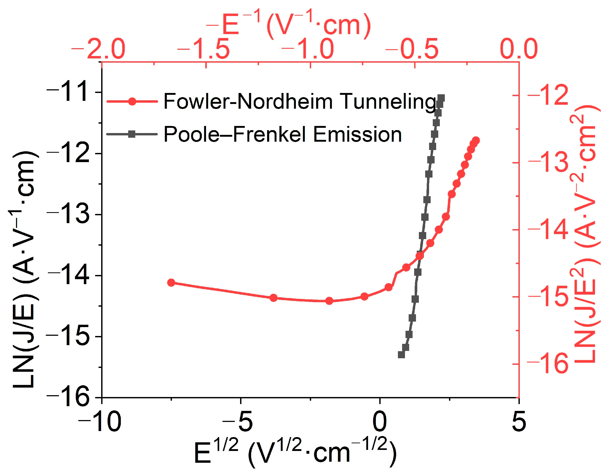
  • Atomic displacement: defects introduced by atomic displacement in SiO2 caused by irradiation.
  • Chemical bond breakage: defects introduced by chemical bond breakage in SiO2 caused by electrical stress.
The PIGS results show that the gate leakage current IGS of the device did not significantly increase when VGS = 0 V or −10 V, indicating that the gate oxide of the devices did not suffer catastrophic damage. Therefore, it is believed that the gate oxide of the devices did not break down due to particle irradiation. Consequently, it is believed that the atomic displacement caused by this injection of heavy ions will not degrade the reliability of the gate oxide of the SiC MOSFET [16]. At this time, gate oxide defects are mainly formed by the breaking of O-Si-O chemical bonds when SiO2 approaches its critical breakdown electric field under high voltage, which causes carriers to pass through the oxide layer via defect-assisted tunneling and to be collected by the gate, thereby causing the breakdown of the gate oxide layer.

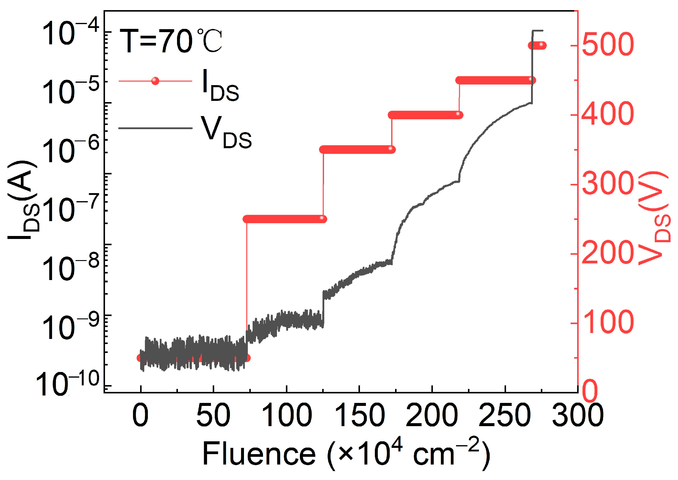
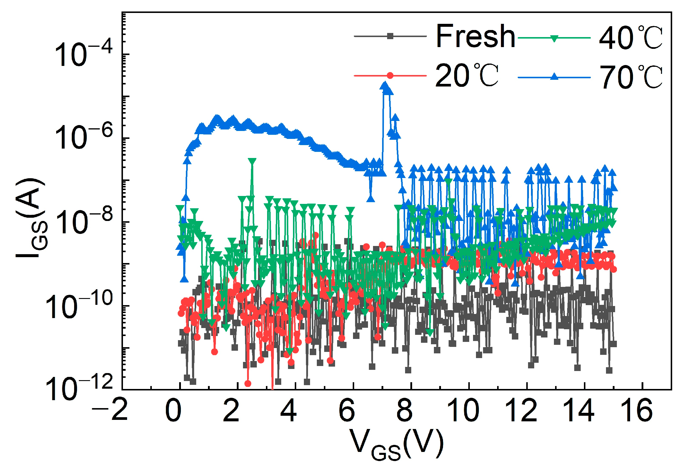
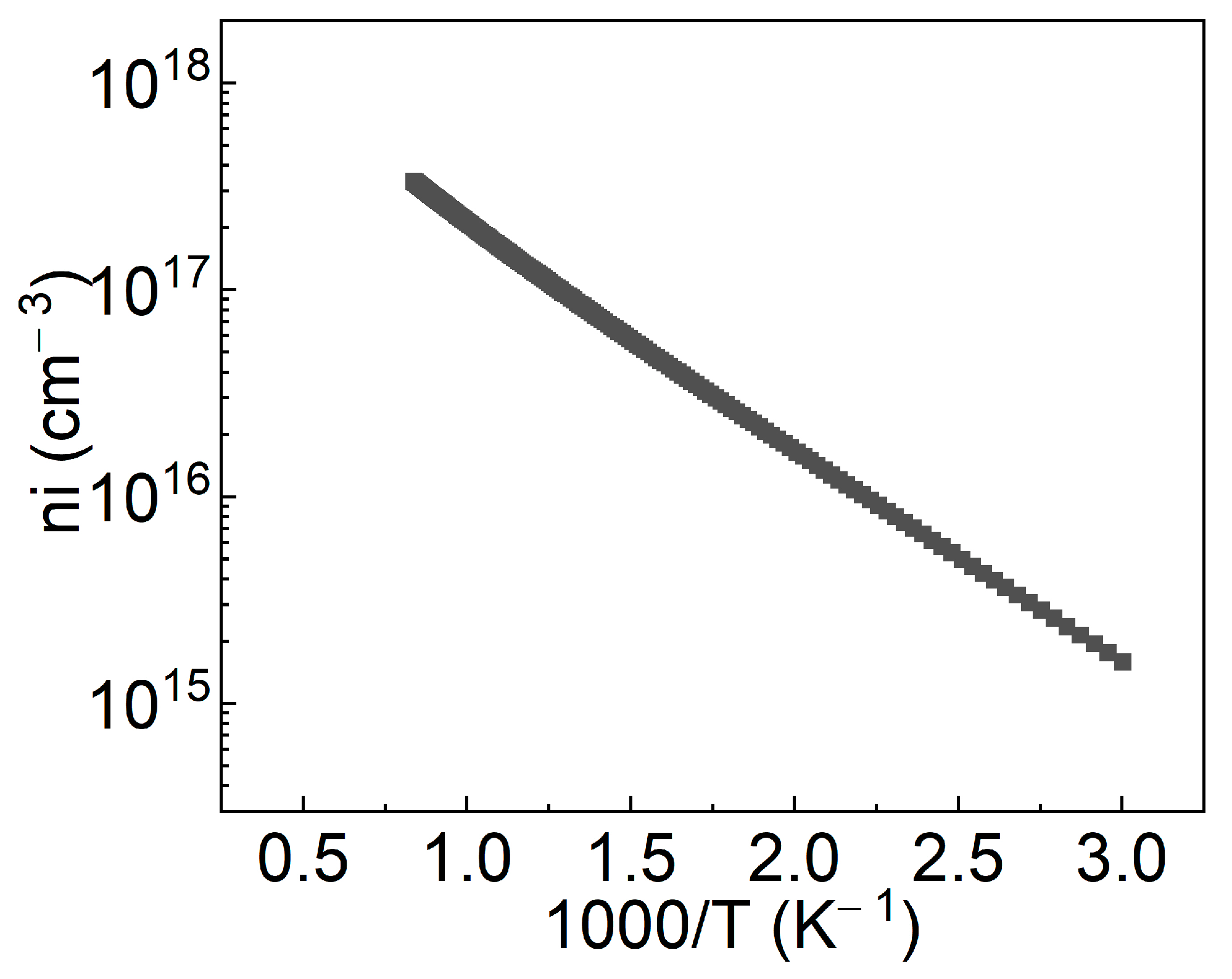
3.2. Temperature Synergy Effect

Different temperature points were selected for the irradiation experiments to explore the relationship between the SEB sensitivity and temperature of the SiC MOSFET. Figure 7 and Figure 8 show that the SEB voltage of the device at 40 °C is 450 V, and the SEB voltage of the device at 70 °C increased by 50 V, which shows that different temperature environments cause the SEB threshold voltage of the sample to change. Furthermore, in the experiment at 70 °C, the experimental SiC MOSFET showed a significant decrease in leakage ID at an early stage. When VDS = 400 V, the ID increased rapidly, by two orders of magnitude, and SEB occurred when VDS was 500 V. However, in the 40 °C environment, the leakage current of the sample increased rapidly when the VDS was 450 V, and it was determined that SEB occurred. This phenomenon shows that with increases in the working environment temperature of the SiC MOSFET, the SEB threshold voltage increases. Additionally, the SiC MOSFET experiences leakage degradation before the SEB occurs at any temperature when VGS = 0 V.
Based on the PISG test, the relationship between the potential damage degree of the oxide and the environmental temperature was explored. Figure 9 shows the PIGS of the SiC MOSFET with irradiation at different temperatures. The results revealed that the gate leakage current of the SiC MOSFET increased to varying degrees after it was irradiated by heavy ions. However, a high temperature of 70 °C caused the gate leakage current of the device to increase significantly, and it fluctuated violently with increasing gate voltage stress. The leakage current of the SiC MOSFET irradiated at 40 °C was significantly greater than that of the device irradiated at 20 °C. A higher VDS is required for catastrophic SEB damage to the devices at 70 °C, which leads to the generation of a greater instantaneous electric field during its SEB, as well as to more severe gate defects. Combined with Formula (1), it can also be proven that due to the defects introduced by irradiation, the gate leakage current mechanism of the SiC MOSFET changes to a PF emission model. At higher temperatures, the gate oxide layer of the device is more damaged, and the PF emission current increases, resulting in a larger gate leakage current.
Moreover, the threshold voltage of the device was analyzed. For the MOSFET with N-channel enhancement, the source and drain electrodes were connected, with the source voltage being VS and the substrate voltage being VB. When VB = VS = 0 V, Formula (3) is obtained [17]:
V T N = K 2 ϕ f p + ϕ m s Q o x C o x + 2 ϕ f p
where K is the body factor, K = 2 q ε s N A 1 2 C o x , ϕfp is the substrate Fermi potential, ϕms is the metal semiconductor work function difference, Qox is the effective charge surface density of the gate oxide layer, Cox is the gate oxide layer capacitance, q is the absolute value of the electron charge, q = 1.602 × 10⁻¹⁹ C, εs is the dielectric constant, and NA is the doping concentration.
According to Formula (3), the threshold voltage is divided into three main parts:
  • Voltage drop on the gate oxide layer, caused by the charge that generates the strong inversion layer.
  • Flat band voltages. The second and third terms are the flat band voltages of the MOSFET device.
  • The surface potential is ϕs = 2ϕfp, where a strong inversion layer begins to form at the interface. The ϕfp formula can be expressed as follows:
ϕ f p = k T q l n N A n i
For the SiC, the semiempirical formula for the variation in the intrinsic carrier concentration with temperature is as follows:
n i = 1.7 × 10 16 × T 2 3 × e 2.08 × 10 3 T
Equation (5) shows that the intrinsic carrier concentration increases with increases in temperature, as shown in Figure 10. Therefore, increasing the temperature will reduce the substrate Fermi potential, which will lead to a negative drift in the threshold voltage. Therefore, under the same gate-source bias conditions, a high-temperature environment will lead to an increase in the effective electric field of the device channel and an increase in the channel carrier density, which will lead to an increase in the leakage current and an early onset of leakage degradation in a high-temperature environment.

4. Conclusions

Heavy ion irradiation experiments on SiC MOSFETs were carried out, and the performance degradation of SiC MOSFETs under Cl ions irradiation was experimentally studied. The synergistic effects of bias voltage and temperature on the SEB of the SiC MOSFETs were discussed. The research results show that the SEB threshold voltage decreases with increases in the absolute value of the negative bias of the gate-source voltage. Before the occurrence of SEB, the leakage current of the device increases, the leakage degradation becomes more severe with increases in the negative bias of the gate-source voltage, and the slope of the relationship curve between the leakage current and the bias voltage increases. The test results for the latent gate damage show that due to the large negative gate-source voltage, the breakdown of the SiC MOSFET oxide layer changes from FN tunneling to PF emission, so the gate latent damage of the device that has an SEB under a large negative bias is also more serious. The research results for the temperature synergy effect show that due to the increase in temperature, the intrinsic carrier concentration increases, the Fermi potential decreases, the conduction threshold of the SiC MOSFETs decreases, and the SEB threshold voltage increases. However, the SiC MOSFETs experience more severe gate latent damage after irradiation at high temperatures.

Author Contributions

Conceptualization, C.L. and G.G.; methodology, H.S.; software, H.S. and J.H.; validation, H.S., F.L., Z.Z. and J.H.; formal analysis, C.L.; investigation, H.S.; resources, C.L.; data curation, H.S.; writing—original draft preparation, C.L.; writing—review and editing, C.L. and H.S.; visualization, Z.Z.; supervision, Y.Z.; project administration, G.G.; funding acquisition, G.G. All authors have read and agreed to the published version of the manuscript.

Funding

This research received no external funding.

Data Availability Statement

The data used to support the findings of this study are available from the corresponding author upon request.

Acknowledgments

This work was supported through the CNNC’s R&D platform steadily supports scientific research projects (No. WDZC-2023-AW-0201). And all the authors would like to thank the editors and reviewers for their contributions to our manuscript.

Conflicts of Interest

The authors declare no conflicts of interest.

References

  1. Grome, C.A.; Ji, W. A Brief Review of Single-Event Burnout Failure Mechanisms and Design Tolerances of Silicon Carbide Power MOSFETs. Electronics 2024, 13, 1414. [Google Scholar] [CrossRef]
  2. Zhang, H.; Guo, H.; Lei, Z.; Peng, C.; Zhang, Z.; Chen, Z.; Sun, C.; He, Y.; Zhang, F.; Pan, X.; et al. Experiment and Simulation on Degradation and Burnout Mechanisms of SiC MOSFET under Heavy Ion Irradiation. Chin. Phys. B 2023, 32, 028504. [Google Scholar]
  3. Peng, C.; Lei, Z.; Chen, Z.; Yue, S.; Zhang, Z.; He, Y.; Huang, Y. Experimental and Simulation Studies of Radiation-Induced Single Event Burnout in SiC-Based Power MOSFETs. IET Power Electron. 2021, 14, 1700–1712. [Google Scholar]
  4. Martinella, C.; Ziemann, T.; Stark, R.; Tsibizov, A.; Voss, K.O.; Alia, R.G.; Kadi, Y.; Grossner, U.; Javanainen, A. Heavy-Ion Microbeam Studies of Single-Event Leakage Current Mechanism in SiC VD-MOSFETs. IEEE Trans. Nucl. Sci. 2020, 67, 1381–1389. [Google Scholar]
  5. Martinella, C.; Natzke, P.; Alia, R.G.; Kadi, Y.; Niskanen, K.; Rossi, M.; Jaatinen, J.; Kettunen, H.; Tsibizov, A.; Grossner, U.; et al. Heavy-Ion Induced Single Event Effects and Latent Damages in SiC Power MOSFETs. Microelectron. Reliab. 2022, 128, 114423. [Google Scholar]
  6. Kim, C.; Yoon, H.; Kim, D.-S.; Seok, O. Comparison Analysis of Radiation Effects on 1.2 kV SiC Metal-Oxide-Semiconductor Field-Effect Transistors with Gamma-Ray and Proton Irradiation. Electronics 2024, 13, 1352. [Google Scholar] [CrossRef]
  7. Johnson, R.A.; Witulski, A.F.; Ball, D.R.; Galloway, K.F.; Sternberg, A.L.; Reed, R.A.; Schrimpf, R.D.; Alles, M.L.; Lauenstein, J.M.; Hutson, J.M. Analysis of Heavy-Ion-Induced Leakage Current in SiC Power Devices. IEEE Trans. Nucl. Sci. 2022, 69, 248–253. [Google Scholar]
  8. Johnson, R.A.; Witulski, A.F.; Sierawski, B.D.; Ball, D.B.; Galloway, K.F.; Sternberg, A.L.; Reed, R.A.; Schrimpf, R.D.; Alles, M.L.; Lauenstein, J.M.; et al. Influence of Radiation Environment Variability on Cumulative Heavy-Ion-Induced Leakage Current in SiC Power Devices. IEEE Trans. Nucl. Sci. 2023, 70, 322–327. [Google Scholar]
  9. Martinella, C.; Stark, R.; Ziemann, T.; Alia, R.G.; Kadi, Y.; Grossner, U.; Javanainen, A. Current Transport Mechanism for Heavy-Ion Degraded SiC MOSFETs. IEEE Trans. Nucl. Sci. 2019, 66, 1702–1709. [Google Scholar]
  10. Witulski, A.F.; Arslanbekov, R.; Raman, A.; Schrimpf, R.D.; Sternberg, A.L.; Galloway, K.F.; Javanainen, A.; Grider, D.; Lichtenwalner, D.J.; Hull, B. Single-Event Burnout of SiC Junction Barrier Schottky Diode High-Voltage Power Devices. IEEE Trans. Nucl. Sci. 2018, 65, 256–261. [Google Scholar]
  11. Cao, S.; Yu, Q.; Wang, Q.; Wang, H.; Sun, Y.; Lv, H.; Mei, B.; Mo, R.; Li, P.; Zhang, H. Failure Analysis of Heavy Ion-Irradiated Silicon Carbide Junction Barrier Schottky Diodes. Microelectron. Reliab. 2024, 157, 115401-1–115401-5. [Google Scholar]
  12. Pintacuda, F.; Massett, S.; Vitanza, E.; Muschitiello, M.; Cantarella, V. SEGR and PIGS Failure Analysis of SiC Mosfet. In Proceedings of the 2019 European Space Power Conference (ESPC), Juan-les-Pins, France, 30 September–4 October 2019. [Google Scholar]
  13. Rafí, J.M.; Campabadal, F.; Ohyama, H.; Takakura, K.; Tsunoda, I.; Zabala, M.; Beldarrain, O.; González, M.B.; García, H.; Castán, H.; et al. 2 MeV Electron Irradiation Effects on the Electrical Characteristics of Metal-Oxide-Silicon Capacitors with Atomic Layer Deposited Al2IO3, HfO2 and Nanolaminated Dielectrics. Solid State Electron. 2013, 79, 65–74. [Google Scholar]
  14. Lim, E.W.; Ismail, R. Conduction Mechanism of Valence Change Resistive Switching Memory: A Survey. Electronics 2015, 4, 586–613. [Google Scholar] [CrossRef]
  15. Yang, W.L.; Marino, J.; Monson, A.; Wolden, C.A. An Investigation of Annealing on the Dielectric Performance of TiO2 Thin Films. Semicond. Sci. Technol. 2006, 21, 1573–1579. [Google Scholar]
  16. Zhou, X.; Pang, H.; Jia, y.; Hu, D.; Wu, Y.; Zhang, S.; Li, Y.; Li, X.; Wang, L.; Fang, X.; et al. Gate Oxide Damage of SiC MOSFETs Induced by Heavy-Ion Strike. IEEE Trans. Electron Devices 2021, 68, 4010–4015. [Google Scholar]
  17. Chen, X.; Zhang, Q.; Chen, Y. Microelectronic Devices, 4th ed.; Publishing House of Electronics Industry: Beijing, China, 2011; pp. 208–212. [Google Scholar]
Figure 1. The block representation of the experimental setup (G is gate, D is drain, S is source).
Electronics 13 03402 g001
Figure 2. Drain-source current real-time curve (VGS = 0 V).
Electronics 13 03402 g002
Figure 3. Drain-source current real-time curve (VGS = −10 V).
Electronics 13 03402 g003
Figure 4. Drain-source current real-time curve (VGS = −15 V).
Electronics 13 03402 g004
Figure 5. PIGS results of SiC MOSFETs with different VGs (VDS = 0 V).
Electronics 13 03402 g005
Figure 6. ln(J/E)~E1/2 and ln(J/E2)~(−E−1) characteristic curves (VGS = −15 V).
Electronics 13 03402 g006
Figure 7. Drain-source current real-time curve (T = 40 °C).
Electronics 13 03402 g007
Figure 8. Drain-source current real-time curve (T = 70 °C).
Electronics 13 03402 g008
Figure 9. PIGS results of SiC MOSFETs irradiated at different temperatures (VDS = 0 V).
Electronics 13 03402 g009
Figure 10. Relationship between ni and temperature.
Electronics 13 03402 g010
Disclaimer/Publisher’s Note: The statements, opinions and data contained in all publications are solely those of the individual author(s) and contributor(s) and not of MDPI and/or the editor(s). MDPI and/or the editor(s) disclaim responsibility for any injury to people or property resulting from any ideas, methods, instructions or products referred to in the content.

