
2D and Quasi-2D Halide Perovskite-Based Resistive Switching Memory Systems


Abstract
1. Introduction
2. HPs
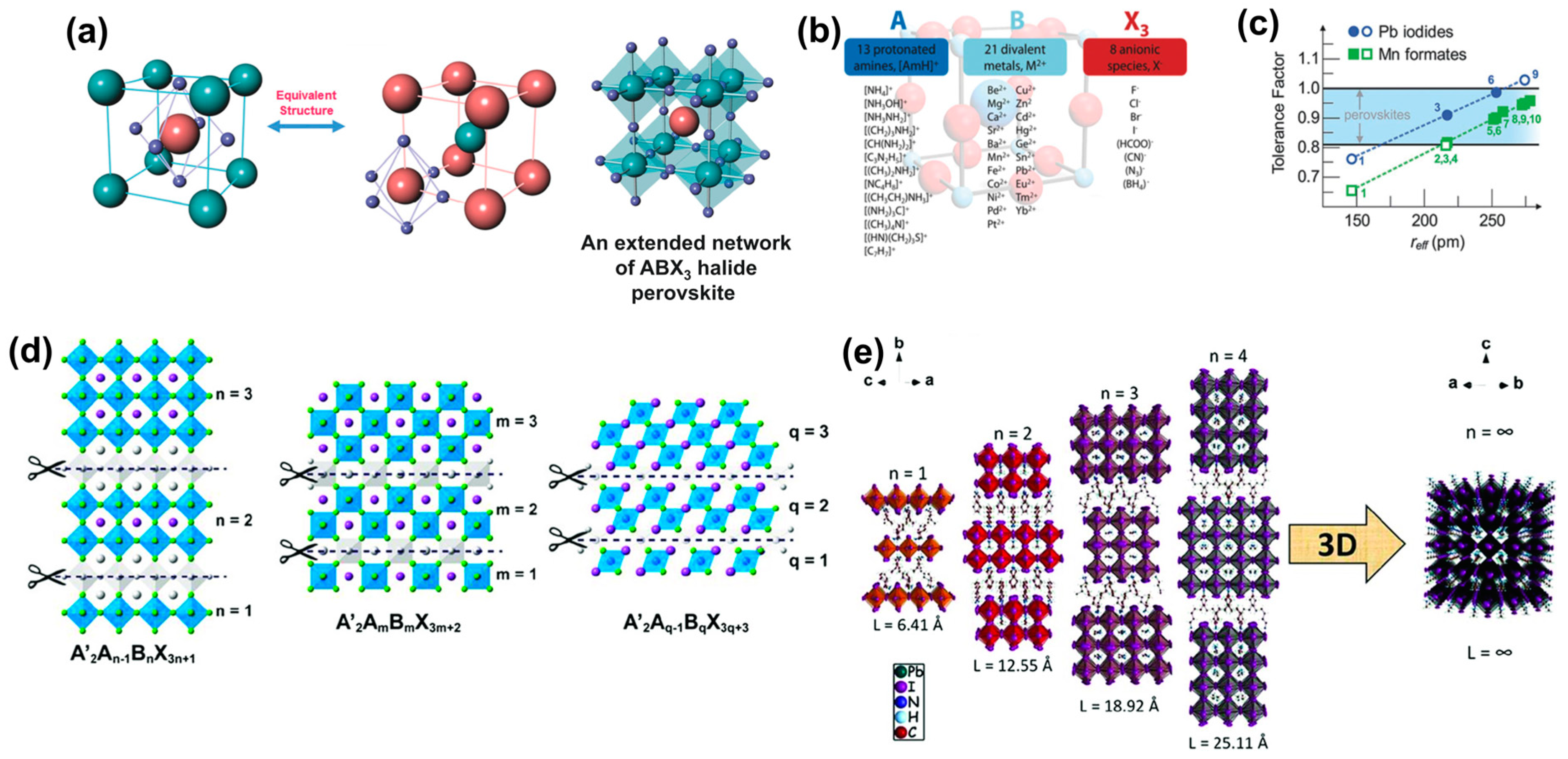
2.1. Structures
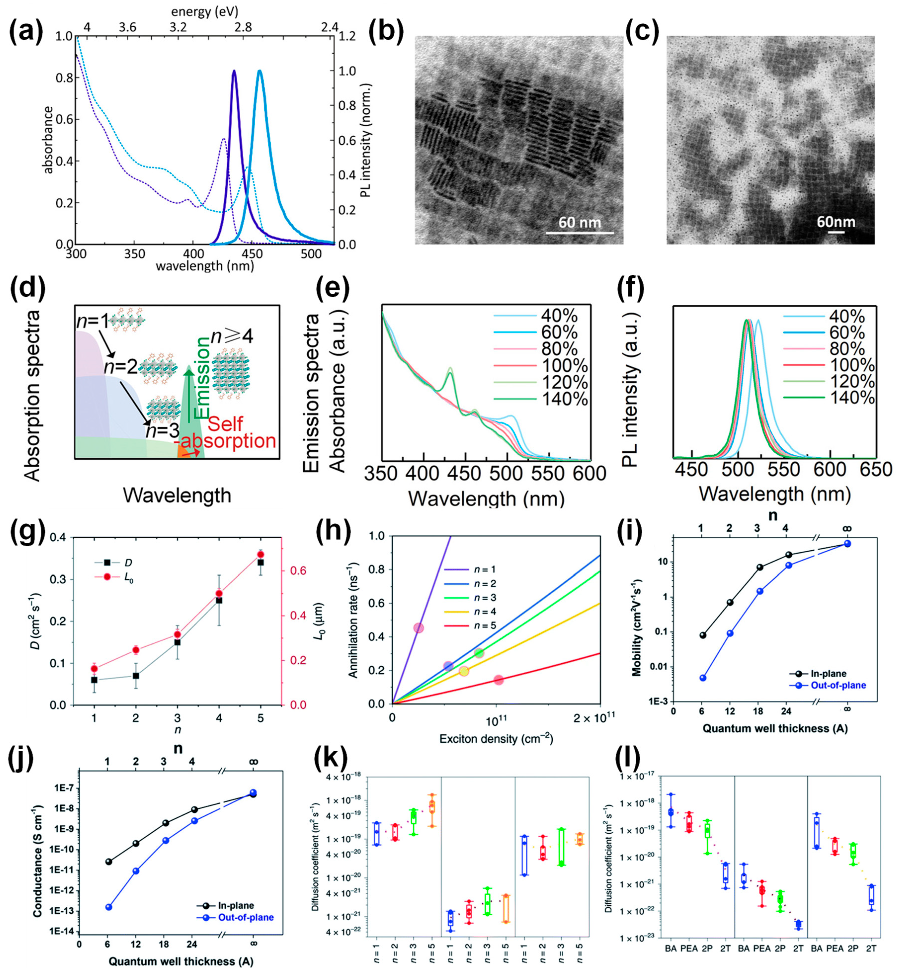
2.2. Photoluminescence (PL)
2.3. Binding Energies
2.4. Charge Transports
3. RS Memory Devices
3.1. The Operating Principles
3.2. Bipolar and Unipolar RS Modes
3.3. The Operational Mechanisms of Resistive Switching Memory Devices
4. HPs-Based RS Memory Devices
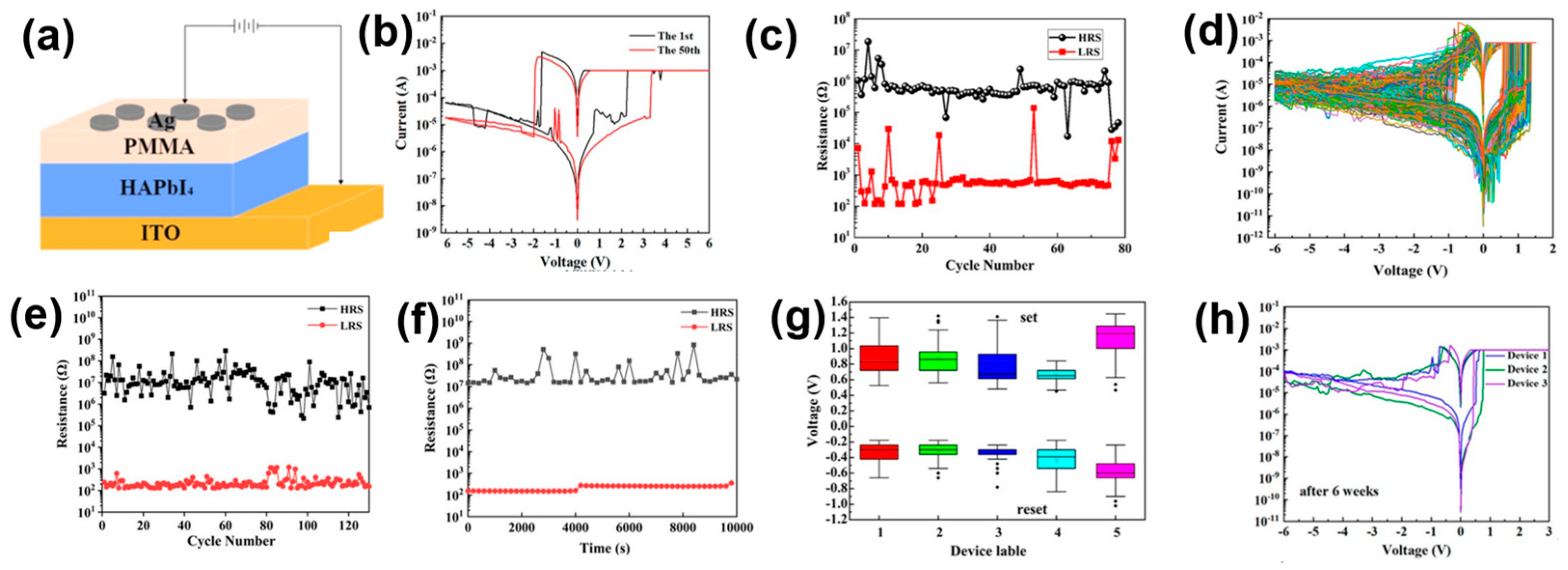
4.1. Two-Dimensional Single Crystal HP-Based RS Memory Devices
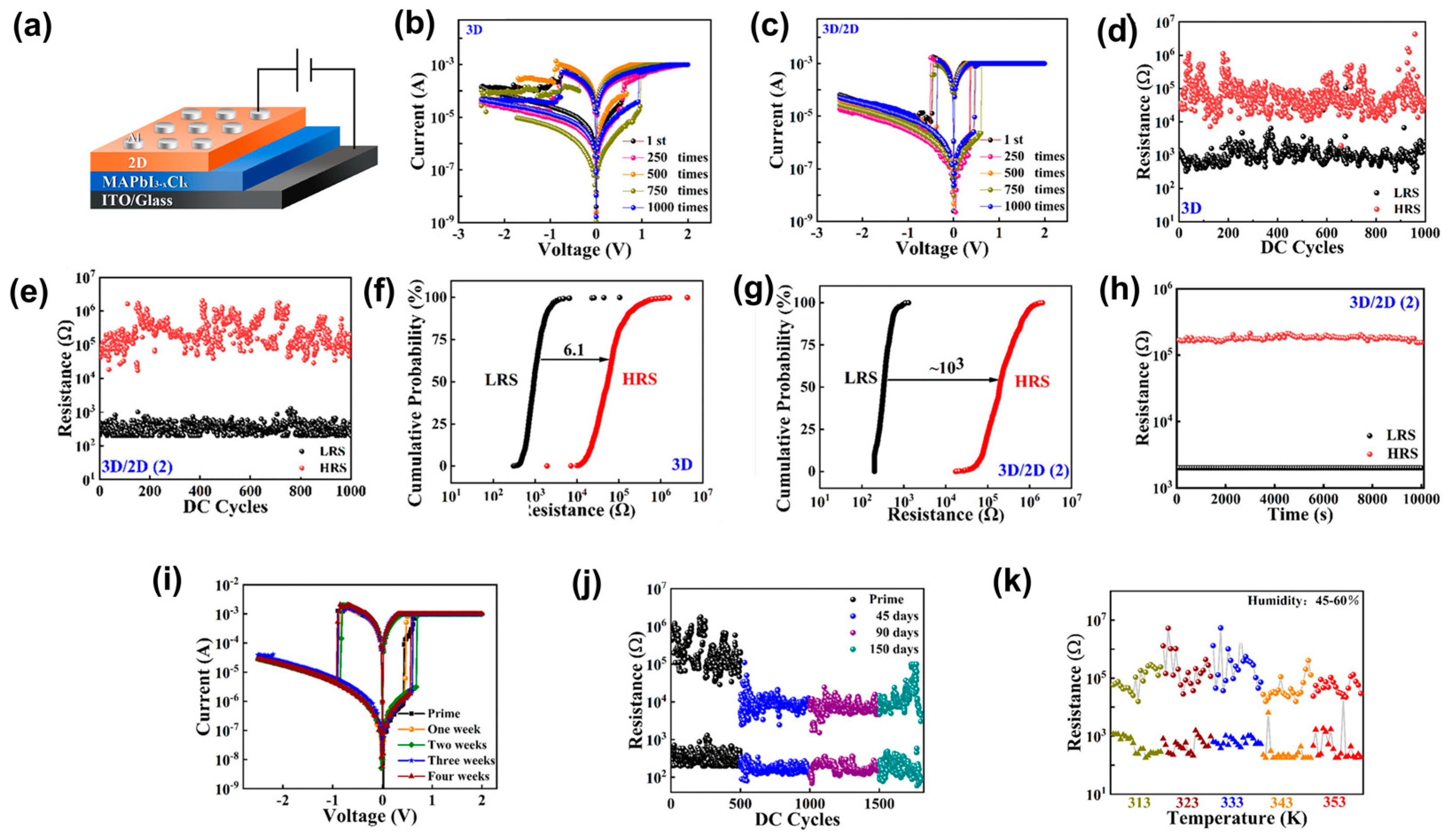
4.2. Two-Dimensional/3D HPs Heterojunction-Based RS Memory Devices
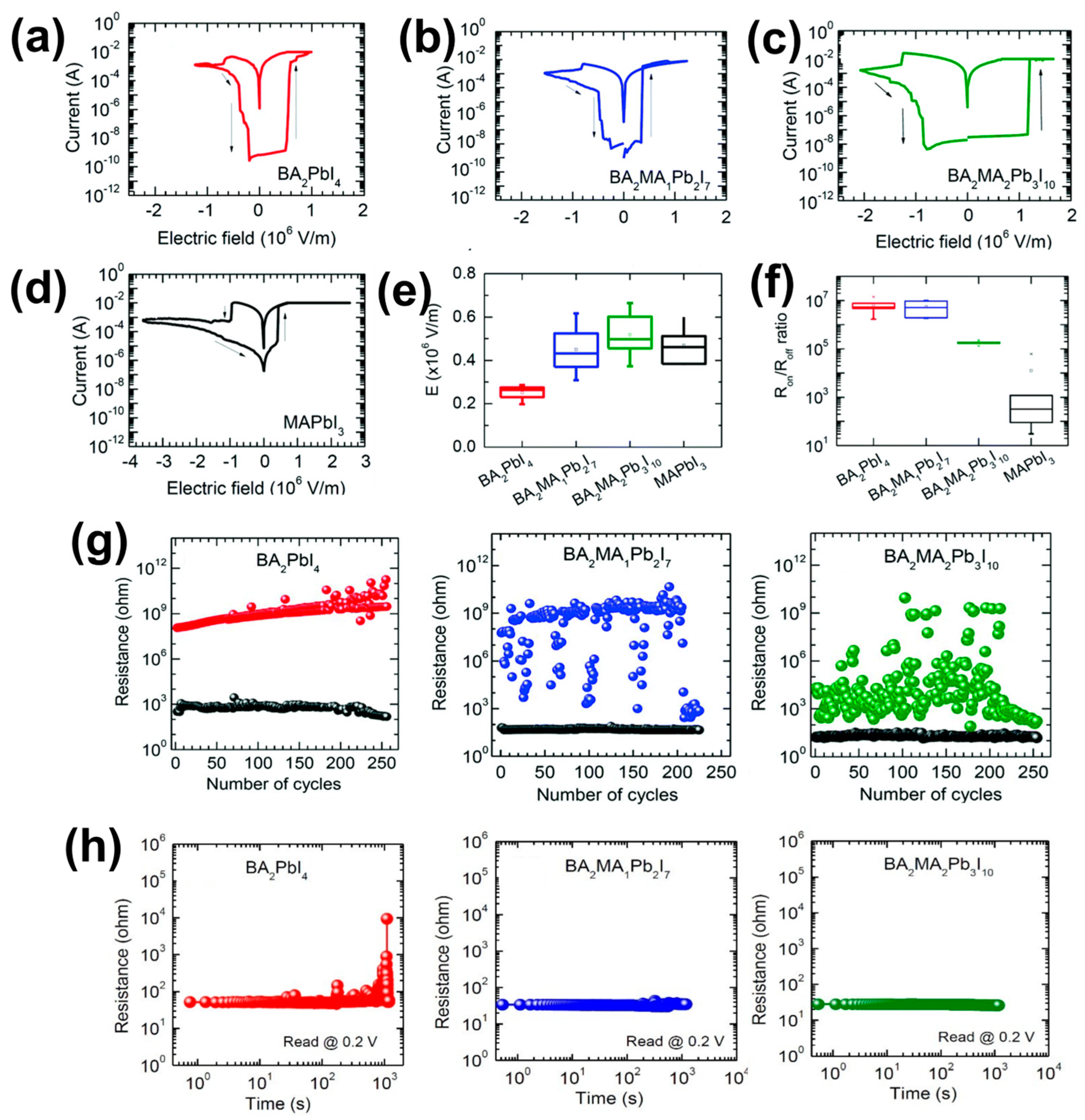
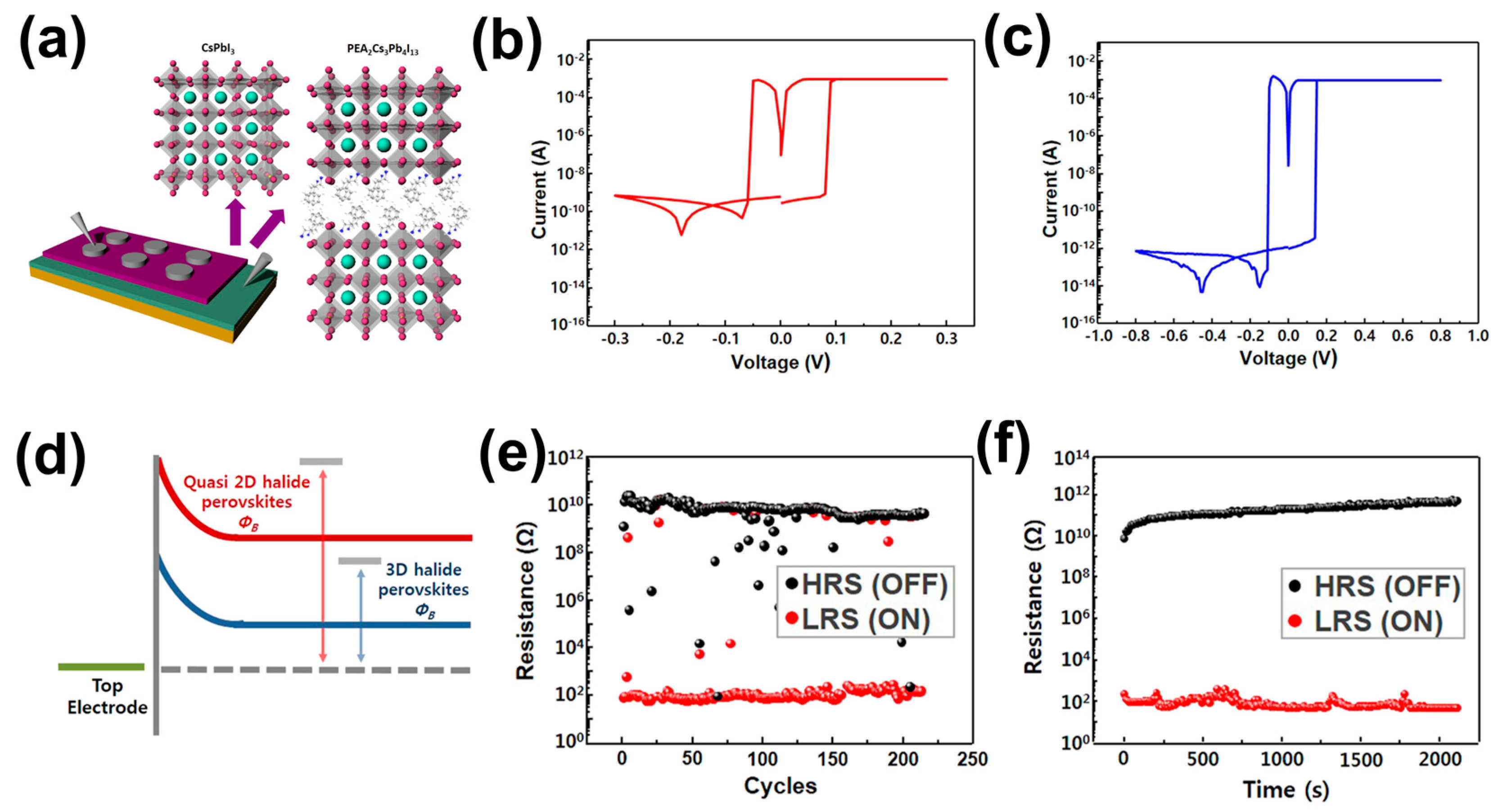
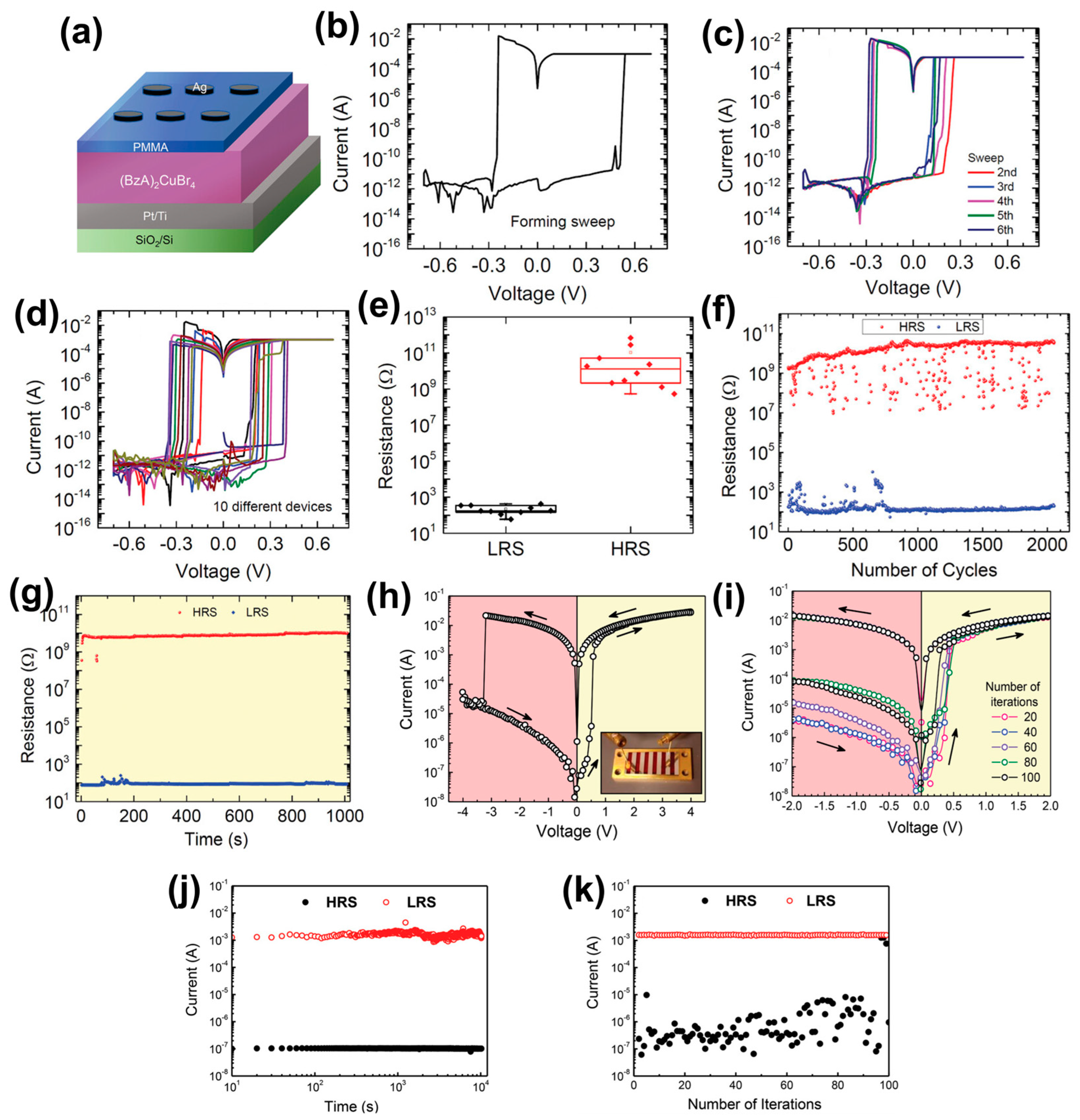
4.3. Two-Dimensional/Quasi-2D HPs-Based RS Memory Devices
4.4. Lead-Free HP-Based RS Memory Devices
5. Conclusions and Perspectives
Author Contributions
Funding
Data Availability Statement
Conflicts of Interest
References
- Kim, H.; Veerappan, G.; Park, J.H. Conducting Polymer Coated Non-Woven Graphite Fiber Film for Dye-Sensitized Solar Cells: Superior Pt- and FTO-Free Counter Electrodes. Electrochim. Acta 2014, 137, 164–168. [Google Scholar] [CrossRef]
- Wang, L.; Huang, L.; Tan, W.C.; Feng, X.; Chen, L.; Huang, X.; Ang, K.W. 2D Photovoltaic Devices: Progress and Prospects. Small Methods 2018, 2, 1700294. [Google Scholar] [CrossRef]
- Kim, H.; Kang, B.K.; Moon, C.W. Refractive Index Modulation for Metal Electrodeposition-Based Active Smart Window Applications. Micromachines 2024, 15, 334. [Google Scholar] [CrossRef]
- Kim, H.; Veerappan, G.; Wang, D.H.; Park, J.H. Large Area Platinum and Fluorine-Doped Tin Oxide-Free Dye Sensitized Solar Cells with Silver-Nanoplate Embedded Poly(3,4-Ethylenedioxythiophene) Counter Electrode. Electrochim. Acta 2016, 187, 218–223. [Google Scholar] [CrossRef]
- Chang, D.W.; Choi, H.J.; Filer, A.; Baek, J.B. Graphene in Photovoltaic Applications: Organic Photovoltaic Cells (OPVs) and Dye-Sensitized Solar Cells (DSSCs). J. Mater. Chem. A Mater. 2014, 2, 12136–12149. [Google Scholar] [CrossRef]
- Roslan, N.; Ya’acob, M.E.; Radzi, M.A.M.; Hashimoto, Y.; Jamaludin, D.; Chen, G. Dye Sensitized Solar Cell (DSSC) Greenhouse Shading: New Insights for Solar Radiation Manipulation. Renew. Sustain. Energy Rev. 2018, 92, 171–186. [Google Scholar] [CrossRef]
- Kim, H.; Han, J.S.; Choi, J.; Kim, S.Y.; Jang, H.W. Halide Perovskites for Applications beyond Photovoltaics. Small Methods 2018, 2, 1700310. [Google Scholar] [CrossRef]
- Qian, J.; Xu, B.; Tian, W. A Comprehensive Theoretical Study of Halide Perovskites ABX3. Org. Electron. 2016, 37, 61–73. [Google Scholar] [CrossRef]
- Lang, L.; Yang, J.H.; Liu, H.R.; Xiang, H.J.; Gong, X.G. First-Principles Study on the Electronic and Optical Properties of Cubic ABX3 Halide Perovskites. Phys. Lett. A 2014, 378, 290–293. [Google Scholar] [CrossRef]
- Murad, K.; Noman, M.; Khan, S.; Neffati, R.; Ashraf, M.W.; Murtaza, G. To Study the Structural, Electronic and Optical Properties of Predicted Stable Halide Perovskites ABX3. Phys. Scr. 2023, 98, 075945. [Google Scholar] [CrossRef]
- Ben Sadok, R.; Plugaru, N.; Birsan, A.; Kuncser, V.; Hammoutène, D. Effect of Chemical Nature of Atoms on the Electronic, Dielectric, and Dynamical Properties of ABX3 Halide Perovskite. Int. J. Quantum Chem. 2020, 120, e26172. [Google Scholar] [CrossRef]
- Akkerman, Q.A.; Manna, L. What Defines a Halide Perovskite? ACS Energy Lett. 2020, 5, 604–610. [Google Scholar] [CrossRef]
- Johnston, M.B.; Herz, L.M. Hybrid Perovskites for Photovoltaics: Charge-Carrier Recombination, Diffusion, and Radiative Efficiencies. Acc. Chem. Res. 2016, 49, 146–154. [Google Scholar] [CrossRef] [PubMed]
- Ma, L.; Hao, F.; Stoumpos, C.C.; Phelan, B.T.; Wasielewski, M.R.; Kanatzidis, M.G. Carrier Diffusion Lengths of over 500 nm in Lead-Free Perovskite CH3NH3SnI3 Films. J. Am. Chem. Soc. 2016, 138, 14750–14755. [Google Scholar] [CrossRef] [PubMed]
- Van Le, Q.; Jang, H.W.; Kim, S.Y. Recent Advances toward High-Efficiency Halide Perovskite Light-Emitting Diodes: Review and Perspective. Small Methods 2018, 2, 1700419. [Google Scholar] [CrossRef]
- Lin, Y.H.; Pattanasattayavong, P.; Anthopoulos, T.D. Metal-Halide Perovskite Transistors for Printed Electronics: Challenges and Opportunities. Adv. Mater. 2017, 29, 1702838. [Google Scholar] [CrossRef] [PubMed]
- He, S.; Yu, X.; Wang, J.; Zhong, W.K.; Cheng, B.; Zhao, J. Attaining Inhibition of Sneak Current and Versatile Logic Operations in a Singular Halide Perovskite Memristive Device by Introducing Appropriate Interface Barriers. Nanoscale 2023, 16, 1102–1114. [Google Scholar] [CrossRef]
- Zhou, F.; Li, Z.; Lan, W.; Wang, Q.; Ding, L.; Jin, Z. Halide Perovskite, a Potential Scintillator for X-Ray Detection. Small Methods 2020, 4, 2000506. [Google Scholar] [CrossRef]
- Han, B.; Zhao, J.; Luo, Z.; Cai, F.; Yuan, Z.; Zeng, H. Energy Storage Research of Metal Halide Perovskites for Rechargeable Batteries. Nano Energy 2023, 115, 108646. [Google Scholar] [CrossRef]
- Kim, H.; Huynh, K.A.; Kim, S.Y.; Van Le, Q.; Jang, H.W. 2D and Quasi-2D Halide Perovskites: Applications and Progress. Phys. Status Solidi Rapid Res. Lett. 2020, 14, 1900435. [Google Scholar] [CrossRef]
- Park, J.Y.; Lee, Y.H.; Kim, H.; Dou, L. Two-Dimensional Perovskite Heterostructures for Single Crystal Semiconductor Devices. J. Appl. Phys. 2023, 134, 060901. [Google Scholar] [CrossRef]
- Kim, H.; Han, J.S.; Kim, S.G.; Kim, S.Y.; Jang, H.W. Halide Perovskites for Resistive Random-Access Memories. J. Mater. Chem. C 2019, 7, 5226–5234. [Google Scholar] [CrossRef]
- Tyagi, P.; Arveson, S.M.; Tisdale, W.A. Colloidal Organohalide Perovskite Nanoplatelets Exhibiting Quantum Confinement. J. Phys. Chem. Lett. 2015, 6, 1911–1916. [Google Scholar] [CrossRef] [PubMed]
- Ha, S.T.; Liu, X.; Zhang, Q.; Giovanni, D.; Sum, T.C.; Xiong, Q. Synthesis of Organic-Inorganic Lead Halide Perovskite Nanoplatelets: Towards High-Performance Perovskite Solar Cells and Optoelectronic Devices. Adv. Opt. Mater. 2014, 2, 838–844. [Google Scholar] [CrossRef]
- Xu, X.; Pan, Y.; Zhong, Y.; Ran, R.; Shao, Z. Ruddlesden-Popper Perovskites in Electrocatalysis. Mater. Horiz. 2020, 7, 2519–2565. [Google Scholar] [CrossRef]
- Yu, Y.; Zhang, D.; Yang, P. Ruddlesden-Popper Phase in Two-Dimensional Inorganic Halide Perovskites: A Plausible Model and the Supporting Observations. Nano Lett. 2017, 17, 5489–5494. [Google Scholar] [CrossRef]
- Gong, J.; Hao, M.; Zhang, Y.; Liu, M.; Zhou, Y. Layered 2D Halide Perovskites beyond the Ruddlesden-Popper Phase: Tailored Interlayer Chemistries for High-Performance Solar Cells. Angew. Chem. Int. Ed. 2022, 61, e202112022. [Google Scholar] [CrossRef]
- Li, F.; Xie, Y.; Hu, Y.; Long, M.; Zhang, Y.; Xu, J.; Qin, M.; Lu, X.; Liu, M. Effects of Alkyl Chain Length on Crystal Growth and Oxidation Process of Two-Dimensional Tin Halide Perovskites. ACS Energy Lett. 2020, 5, 1422–1429. [Google Scholar] [CrossRef]
- González-Carrero, S.; Galian, R.E.; Pérez-Prieto, J. Organometal Halide Perovskites: Bulk Low-Dimension Materials and Nanoparticles. Part. Part. Syst. Charact. 2015, 32, 709–720. [Google Scholar] [CrossRef]
- Cinquino, M.; Fieramosca, A.; Mastria, R.; Polimeno, L.; Moliterni, A.; Olieric, V.; Matsugaki, N.; Panico, R.; De Giorgi, M.; Gigli, G.; et al. Managing Growth and Dimensionality of Quasi 2D Perovskite Single-Crystalline Flakes for Tunable Excitons Orientation. Adv. Mater. 2021, 33, 2102326. [Google Scholar] [CrossRef]
- Singldinger, A.; Gramlich, M.; Gruber, C.; Lampe, C.; Urban, A.S. Nonradiative Energy Transfer between Thickness-Controlled Halide Perovskite Nanoplatelets. ACS Energy Lett. 2020, 5, 1380–1385. [Google Scholar] [CrossRef] [PubMed]
- Liu, N.; Luo, J.; Guo, Q.; Du, P.; Gao, L.; Niu, G.; Song, B.; Tang, J. Reduced Self-Absorption of Quasi-2D Perovskites and Their Application in Color Conversion Layers. Adv. Opt. Mater. 2023, 11, 2202118. [Google Scholar] [CrossRef]
- Deng, S.; Shi, E.; Yuan, L.; Jin, L.; Dou, L.; Huang, L. Long-Range Exciton Transport and Slow Annihilation in Two-Dimensional Hybrid Perovskites. Nat. Commun. 2020, 11, 664. [Google Scholar] [CrossRef] [PubMed]
- Wang, K.; Wu, C.; Yang, D.; Jiang, Y.; Priya, S. Quasi-Two-Dimensional Halide Perovskite Single Crystal Photodetector. ACS Nano 2018, 12, 4919–4929. [Google Scholar] [CrossRef] [PubMed]
- Akriti; Shi, E.; Shiring, S.B.; Yang, J.; Atencio-Martinez, C.L.; Yuan, B.; Hu, X.; Gao, Y.; Finkenauer, B.P.; Pistone, A.J.; et al. Layer-by-Layer Anionic Diffusion in Two-Dimensional Halide Perovskite Vertical Heterostructures. Nat. Nanotechnol. 2021, 16, 584–591. [Google Scholar] [CrossRef]
- Etgar, L. The Merit of Perovskite’s Dimensionality; Can This Replace the 3D Halide Perovskite? Energy Environ. Sci. 2018, 11, 234–242. [Google Scholar] [CrossRef]
- Blancon, J.C.; Stier, A.V.; Tsai, H.; Nie, W.; Stoumpos, C.C.; Traoré, B.; Pedesseau, L.; Kepenekian, M.; Katsutani, F.; Noe, G.T.; et al. Scaling Law for Excitons in 2D Perovskite Quantum Wells. Nat. Commun. 2018, 9, 2254. [Google Scholar] [CrossRef]
- Zalamai, V.V.; Syrbu, N.N.; Stamov, I.G.; Beril, S.I. Wannier-Mott Excitons in GaSe Single Crystals. J. Opt. 2020, 22, 085402. [Google Scholar] [CrossRef]
- Agranovich, V.M.; Basko, D.M.; Schmidt, K.; LaRocca, G.C.; Bassani, F.; Forrest, S.; Leo, K.; Lidzey, D. Charged Frenkel Excitons in Organic Crystals. Chem. Phys. 2001, 272, 159–169. [Google Scholar] [CrossRef]
- Smith, I.C.; Hoke, E.T.; Solis-Ibarra, D.; McGehee, M.D.; Karunadasa, H.I. A Layered Hybrid Perovskite Solar-Cell Absorber with Enhanced Moisture Stability. Angew. Chem. Int. Ed. 2014, 53, 11232–11235. [Google Scholar] [CrossRef]
- Han, J.S.; Van Le, Q.; Choi, J.; Hong, K.; Moon, C.W.; Kim, T.L.; Kim, H.; Kim, S.Y.; Jang, H.W. Air-Stable Cesium Lead Iodide Perovskite for Ultra-Low Operating Voltage Resistive Switching. Adv. Funct. Mater. 2018, 28, 1705783. [Google Scholar] [CrossRef]
- Ge, J.; Chaker, M. Oxygen Vacancies Control Transition of Resistive Switching Mode in Single-Crystal TiO2 Memory Device. ACS Appl. Mater. Interfaces 2017, 9, 16327–16334. [Google Scholar] [CrossRef] [PubMed]
- Choi, J.; Park, S.; Lee, J.; Hong, K.; Kim, D.H.; Moon, C.W.; Park, G.D.; Suh, J.; Hwang, J.; Kim, S.Y.; et al. Organolead Halide Perovskites for Low Operating Voltage Multilevel Resistive Switching. Adv. Mater. 2016, 28, 6562–6567. [Google Scholar] [CrossRef] [PubMed]
- Schönhals, A.; Rosário, C.M.M.; Hoffmann-Eifert, S.; Waser, R.; Menzel, S.; Wouters, D.J. Role of the Electrode Material on the RESET Limitation in Oxide ReRAM Devices. Adv. Electron. Mater. 2018, 4, 1700243. [Google Scholar] [CrossRef]
- Kwak, K.J.; Lee, D.E.; Kim, S.J.; Jang, H.W. Halide Perovskites for Memristive Data Storage and Artificial Synapses. J. Phys. Chem. Lett. 2021, 12, 8999–9010. [Google Scholar] [CrossRef] [PubMed]
- Di, J.; Du, J.; Lin, Z.; Liu, S.; Ouyang, J.; Chang, J. Recent Advances in Resistive Random Access Memory Based on Lead Halide Perovskite. InfoMat 2021, 3, 293–315. [Google Scholar] [CrossRef]
- Jeong, D.N.; Yang, J.M.; Park, N.G. Roadmap on Halide Perovskite and Related Devices. Nanotechnology 2020, 31, 152001. [Google Scholar] [CrossRef]
- Choi, J.; Han, J.S.; Hong, K.; Kim, S.Y.; Jang, H.W. Organic-Inorganic Hybrid Halide Perovskites for Memories, Transistors, and Artificial Synapses. Adv. Mater. 2018, 30, e1704002. [Google Scholar] [CrossRef]
- Prakash, A.; Jana, D.; Maikap, S. TaOx-Based Resistive Switching Memories: Prospective and Challenges. Nanoscale Res. Lett. 2013, 8, 1–17. [Google Scholar] [CrossRef]
- Thien, G.S.H.; Sarjidan, M.A.M.; Talik, N.A.; Goh, B.T.; Yap, B.K.; He, Z.; Chan, K.Y. Electrode Dependence in Halide Perovskite Memories: Resistive Switching Behaviours. Mater. Chem. Front. 2022, 6, 3125–3142. [Google Scholar] [CrossRef]
- Satapathi, S.; Raj, K.; Yukta; Afroz, M.A. Halide-Perovskite-Based Memristor Devices and Their Application in Neuromorphic Computing. Phys. Rev. Appl. 2022, 18, 017001. [Google Scholar] [CrossRef]
- How, G.T.S.; Talik, N.A.; Yap, B.K.; Nakajima, H.; Tunmee, S.; Goh, B.T. Multiple Resistive Switching Behaviours of CH3NH3PbI3 Perovskite Film with Different Metal Electrodes. Appl. Surf. Sci. 2019, 473, 194–202. [Google Scholar] [CrossRef]
- Nowak, E.; Chłopocka, E.; Szybowicz, M. ZnO and ZnO-Based Materials as Active Layer in Resistive Random-Access Memory (RRAM). Crystals 2023, 13, 416. [Google Scholar] [CrossRef]
- Poddar, S.; Zhang, Y.; Chen, Z.; Ma, Z.; Fu, Y.; Ding, Y.; Chan, C.L.J.; Zhang, Q.; Zhang, D.; Song, Z.; et al. Image Processing with a Multi-Level Ultra-Fast Three Dimensionally Integrated Perovskite Nanowire Array. Nanoscale Horiz. 2022, 7, 759–769. [Google Scholar] [CrossRef]
- Wu, M.C.; Ting, Y.H.; Chen, J.Y.; Wu, W.W. Low Power Consumption Nanofilamentary ECM and VCM Cells in a Single Sidewall of High-Density VRRAM Arrays. Adv. Sci. 2019, 6, 1902363. [Google Scholar] [CrossRef] [PubMed]
- Michieletti, F.; Chen, S.; Weber, C.; Ricciardi, C.; Ohno, T.; Valov, I. Influence of Active Electrode Impurity on Memristive Characteristics of ECM Devices. J. Solid State Electrochem. 2024, 28, 1735–1741. [Google Scholar] [CrossRef]
- Von Witzleben, M.; Hennen, T.; Kindsmüller, A.; Menzel, S.; Waser, R.; Böttger, U. Study of the SET Switching Event of VCM-Based Memories on a Picosecond Timescale. J. Appl. Phys. 2020, 127, 204501. [Google Scholar] [CrossRef]
- Ahn, J.; Bang, J.; Kim, Y.M.; Oh, S.; Kim, S.Y.; Sung, Y.M.; Oh, S.J. Designing Metal Halide Perovskite Nanoparticle-Based Resistive Random-Access Memory Devices through Chemical Treatments. Mater. Today Nano 2023, 24, 100388. [Google Scholar] [CrossRef]
- Lübben, M.; Valov, I. Active Electrode Redox Reactions and Device Behavior in ECM Type Resistive Switching Memories. Adv. Electron. Mater. 2019, 5, 1800933. [Google Scholar] [CrossRef]
- Lv, H.; Xu, X.; Liu, H.; Liu, R.; Liu, Q.; Banerjee, W.; Sun, H.; Long, S.; Li, L.; Liu, M. Evolution of Conductive Filament and Its Impact on Reliability Issues in Oxide-Electrolyte Based Resistive Random Access Memory. Sci. Rep. 2015, 5, 7764. [Google Scholar] [CrossRef]
- Kim, S.G.; Van Le, Q.; Han, J.S.; Kim, H.; Choi, M.J.; Lee, S.A.; Kim, T.L.; Kim, S.B.; Kim, S.Y.; Jang, H.W. Dual-Phase All-Inorganic Cesium Halide Perovskites for Conducting-Bridge Memory-Based Artificial Synapses. Adv. Funct. Mater. 2019, 29, 1906686. [Google Scholar] [CrossRef]
- Waser, R.; Menzel, S.; Rana, V. Recent Progress in Redox-Based Resistive Switching. In Proceedings of the 2012 IEEE International Symposium on Circuits and Systems, Seoul, Republic of Korea, 20–23 May 2012; pp. 1596–1599. [Google Scholar]
- Cuhadar, C.; Kim, S.-G.; Yang, J.-M.; Seo, J.-Y.; Lee, D.; Park, N.-G. All-Inorganic Bismuth Halide Perovskite-Like Materials A3Bi2I9 and A3Bi1.8Na0.2I8.6 (A = Rb and Cs) for Low-Voltage Switching Resistive Memory. ACS Appl. Mater. Interfaces 2018, 10, 29741–29749. [Google Scholar] [CrossRef] [PubMed]
- Valov, I. Interfacial Interactions and Their Impact on Redox-Based Resistive Switching Memories (ReRAMs). Semicond. Sci. Technol. 2017, 32, 093006. [Google Scholar] [CrossRef]
- Kim, W.; Wouters, D.J.; Menzel, S.; Rodenbucher, C.; Waser, R.; Rana, V. Lowering Forming Voltage and Forming-Free Behavior of Ta2O5 ReRAM Devices. In Proceedings of the 2016 46th European Solid-State Device Research Conference (ESSDERC), Lausanne, Switzerland, 12–15 September 2016; pp. 164–167. [Google Scholar]
- Praveen, P.; Rose, T.P.; Saji, K.J. Top Electrode Dependent Resistive Switching in M/ZnO/ITO Memristors, M = Al, ITO, Cu, and Au. Microelectron. J. 2022, 121, 105388. [Google Scholar] [CrossRef]
- Fra, V.; Shahrabi, E.; Leblebici, Y.; Ricciardi, C. Investigation on the Stabilizing Effect of Titanium in HfO2-Based Resistive Switching Devices with Tungsten Electrode. Front. Nanotechnol. 2020, 2, 592684. [Google Scholar] [CrossRef]
- Valov, I.; Waser, R. Comment on Real-Time Observation on Dynamic Growth/Dissolution of Conductive Filaments in Oxide-Electrolyte-Based ReRAM. Adv. Mater. 2013, 25, 162–164. [Google Scholar] [CrossRef]
- Kim, S.G.; Han, J.S.; Kim, H.; Kim, S.Y.; Jang, H.W. Recent Advances in Memristive Materials for Artificial Synapses. Adv. Mater. Technol. 2018, 3, 1800457. [Google Scholar] [CrossRef]
- Han, J.S.; Van Le, Q.; Choi, J.; Kim, H.; Kim, S.G.; Hong, K.; Moon, C.W.; Kim, T.L.; Kim, S.Y.; Jang, H.W. Lead-Free All-Inorganic Cesium Tin Iodide Perovskite for Filamentary and Interface-Type Resistive Switching toward Environment-Friendly and Temperature-Tolerant Nonvolatile Memories. ACS Appl. Mater. Interfaces 2019, 11, 8155–8163. [Google Scholar] [CrossRef]
- Han, J.S.; Van Le, Q.; Kim, H.; Lee, Y.J.; Lee, D.E.; Im, I.H.; Lee, M.K.; Kim, S.J.; Kim, J.; Kwak, K.J.; et al. Lead-Free Dual-Phase Halide Perovskites for Preconditioned Conducting-Bridge Memory. Small 2020, 16, 2003225. [Google Scholar] [CrossRef]
- Chauhan, M.; Singh, R.; Sharma, S.K. Electro-Optically Tunable Passivated Double-Cation Perovskite-Based ReRAM for Low-Power Memory Applications. ACS Appl. Electron. Mater. 2024, 6, 2709–2719. [Google Scholar] [CrossRef]
- Zhou, C.; Tarasov, A.B.; Goodilin, E.A.; Chen, P.; Wang, H.; Chen, Q. Recent Strategies to Improve Moisture Stability in Metal Halide Perovskites Materials and Devices. J. Energy Chem. 2022, 65, 219–235. [Google Scholar] [CrossRef]
- DI, J.; Lin, Z.; Su, J.; Wang, J.; Zhang, J.; Liu, S.; Chang, J.; Hao, Y. Two-Dimensional (C6H5C2H4NH3)2PbI4 Perovskite Single Crystal Resistive Switching Memory Devices. IEEE Electron. Device Lett. 2021, 42, 327–330. [Google Scholar] [CrossRef]
- Liu, B.; Lai, J.; Wu, D.; Li, L.; Kang, K.; Hu, W.; Tang, X. High-Performance Resistive Random Access Memories Based on Two-Dimensional HAPbI4 Organic-Inorganic Hybrid Perovskite. J. Phys. Chem. Lett. 2022, 13, 7653–7659. [Google Scholar] [CrossRef] [PubMed]
- Xia, F.; Xu, Y.; Li, B.; Hui, W.; Zhang, S.; Zhu, L.; Xia, Y.; Chen, Y.; Huang, W. Improved Performance of CH3NH3PbI3-XClx Resistive Switching Memory by Assembling 2D/3D Perovskite Heterostructures. ACS Appl. Mater. Interfaces 2020, 12, 1543–15445. [Google Scholar] [CrossRef] [PubMed]
- Lee, S.M.; Kim, H.; Kim, D.H.; Kim, W.B.; Lee, J.M.; Choi, J.; Shin, H.; Han, G.S.; Jang, H.W.; Jung, H.S. Tailored 2D/3D Halide Perovskite Heterointerface for Substantially Enhanced Endurance in Conducting Bridge Resistive Switching Memory. ACS Appl. Mater. Interfaces 2020, 12, 17039–17045. [Google Scholar] [CrossRef]
- Kim, H.S.; Lee, C.R.; Im, J.H.; Lee, K.B.; Moehl, T.; Marchioro, A.; Moon, S.J.; Humphry-Baker, R.; Yum, J.H.; Moser, J.E.; et al. Lead Iodide Perovskite Sensitized All-Solid-State Submicron Thin Film Mesoscopic Solar Cell with Efficiency Exceeding 9%. Sci. Rep. 2012, 2, 591. [Google Scholar] [CrossRef]
- Burschka, J.; Pellet, N.; Moon, S.J.; Humphry-Baker, R.; Gao, P.; Nazeeruddin, M.K.; Grätzel, M. Sequential Deposition as a Route to High-Performance Perovskite-Sensitized Solar Cells. Nature 2013, 499, 316–319. [Google Scholar] [CrossRef]
- Jeon, N.J.; Noh, J.H.; Kim, Y.C.; Yang, W.S.; Ryu, S.; Seok, S. Il Solvent Engineering for High-Performance Inorganic-Organic Hybrid Perovskite Solar Cells. Nat. Mater. 2014, 13, 897–903. [Google Scholar] [CrossRef]
- Bai, Y.; Xiao, S.; Hu, C.; Zhang, T.; Meng, X.; Lin, H.; Yang, Y.; Yang, S. Dimensional Engineering of a Graded 3D-2D Halide Perovskite Interface Enables Ultrahigh Voc Enhanced Stability in the p-i-n Photovoltaics. Adv. Energy Mater. 2017, 7, 1701038. [Google Scholar] [CrossRef]
- Li, M.H.; Yeh, H.H.; Chiang, Y.H.; Jeng, U.S.; Su, C.J.; Shiu, H.W.; Hsu, Y.J.; Kosugi, N.; Ohigashi, T.; Chen, Y.A.; et al. Highly Efficient 2D/3D Hybrid Perovskite Solar Cells via Low-Pressure Vapor-Assisted Solution Process. Adv. Mater. 2018, 30, e1801401. [Google Scholar] [CrossRef]
- Chen, P.; Bai, Y.; Wang, S.; Lyu, M.; Yun, J.H.; Wang, L. In Situ Growth of 2D Perovskite Capping Layer for Stable and Efficient Perovskite Solar Cells. Adv. Funct. Mater. 2018, 28, 1706923. [Google Scholar] [CrossRef]
- Pan, X.; Chen, X.; Duan, J.; Long, Y.; Wu, Y.; Tang, J.; Ma, G.; Zhang, J.; Wang, H. Three-Dimensional/Two-Dimensional Perovskite-Resistive Random-Access Memory with Low SET Voltage and High Stability. ACS Appl. Electron. Mater. 2023, 5, 6908–6917. [Google Scholar] [CrossRef]
- Zhang, H.; Zhuang, J.; Liu, X.; Ma, Z.; Guo, H.; Zheng, R.; Zhao, S.; Zhang, F.; Xiao, Z.; Wang, H.; et al. Defect Passivation Strategy for Inorganic CsPbI2Br Perovskite Solar Cell with a High-Efficiency of 16.77%. J. Mater. Sci. Technol. 2021, 82, 40–46. [Google Scholar] [CrossRef]
- Jeong, H.J.; Park, C.; Jeon, H.; Lee, K.N.; Lee, J.; Lim, S.C.; Namkoong, G.; Jeong, M.S. Quasi-2D Halide Perovskite Memory Device Formed by Acid-Base Binary Ligand Solution Composed of Oleylamine and Oleic Acid. ACS Appl. Mater. Interfaces 2021, 13, 40891–40900. [Google Scholar] [CrossRef] [PubMed]
- Seo, J.-Y.; Choi, J.; Kim, H.-S.; Kim, J.; Yang, J.-M.; Cuhadar, C.; Han, J.S.; Kim, S.-J.; Lee, D.; Jang, H.W.; et al. Wafer-Scale Reliable Switching Memory Based on 2-Dimensional Layered Organic-Inorganic Halide Perovskite. Nanoscale 2017, 9, 15278–15285. [Google Scholar] [CrossRef]
- Kim, K.M.; Jeong, D.S.; Hwang, C.S. Nanofilamentary Resistive Switching in Binary Oxide System; a Review on the Present Status and Outlook. Nanotechnology 2011, 22, 254002. [Google Scholar] [CrossRef]
- Kim, H.; Choi, M.J.; Suh, J.M.; Han, J.S.; Kim, S.G.; Van Le, Q.; Kim, S.Y.; Jang, H.W. Quasi-2D Halide Perovskites for Resistive Switching Devices with ON/OFF Ratios above 109. NPG Asia Mater. 2020, 12, 21. [Google Scholar] [CrossRef]
- Ng, Y.F.; Kulkarni, S.A.; Parida, S.; Jamaludin, N.F.; Yantara, N.; Bruno, A.; Soci, C.; Mhaisalkar, S.; Mathews, N. Highly Efficient Cs-Based Perovskite Light-Emitting Diodes Enabled by Energy Funnelling. Chem. Commun. 2017, 53, 12004–12007. [Google Scholar] [CrossRef]
- Gebhardt, J.; Kim, Y.; Rappe, A.M. Influence of the Dimensionality and Organic Cation on Crystal and Electronic Structure of Organometallic Halide Perovskites. J. Phys. Chem. C 2017, 121, 6569–6574. [Google Scholar] [CrossRef]
- Ma, S.; Cai, M.; Cheng, T.; Ding, X.; Shi, X.; Alsaedi, A.; Hayat, T.; Ding, Y.; Tan, Z.; Dai, S. Two-Dimensional Organic-Inorganic Hybrid Perovskite: From Material Properties to Device Applications. Sci. China Mater. 2018, 61, 1257–1277. [Google Scholar] [CrossRef]
- Park, J.; Biju, K.P.; Jung, S.; Lee, W.; Lee, J.; Kim, S.; Park, S.; Shin, J.; Hwang, H. Multibit Operation of TiOx-Based ReRAM by Schottky Barrier Height Engineering. IEEE Electron. Device Lett. 2011, 32, 476–478. [Google Scholar] [CrossRef]
- Chen, S.C.; Lou, J.C.; Chien, C.H.; Liu, P.T.; Chang, T.C. An Interfacial Investigation of High-Dielectric Constant Material Hafnium Oxide on Si Substrate. Thin Solid Films 2005, 488, 167–172. [Google Scholar] [CrossRef]
- Kim, Y.; Baik, S.J.; Shin, H. Vertically Oriented 2D Layered Perovskite-Based Resistive Random Access Memory (ReRAM) Crossbar Arrays. Curr. Appl. Phys. 2022, 44, 46–54. [Google Scholar] [CrossRef]
- Kim, S.Y.; Yang, J.M.; Choi, E.S.; Park, N.G. Layered (C6H5CH2NH3)2CuBr4 Perovskite for Multilevel Storage Resistive Switching Memory. Adv. Funct. Mater. 2020, 30, 2002653. [Google Scholar] [CrossRef]
- Paramanik, S.; Maiti, A.; Chatterjee, S.; Pal, A.J. Large Resistive Switching and Artificial Synaptic Behaviors in Layered Cs3Sb2I9 Lead-Free Perovskite Memory Devices. Adv. Electron. Mater. 2022, 8, 2100237. [Google Scholar] [CrossRef]
- Berruet, M.; Pérez-Martínez, J.C.; Romero, B.; Gonzales, C.; Al-Mayouf, A.M.; Guerrero, A.; Bisquert, J. Physical Model for the Current−Voltage Hysteresis and Impedance of Halide Perovskite Memristors. ACS Energy Lett. 2022, 7, 1214–1222. [Google Scholar] [CrossRef]
- Bisquert, J.; Bou, A.; Guerrero, A.; Hernández-Balaguera, E. Resistance Transient Dynamics in Switchable Perovskite Memristors. APL Mach. Learn. 2023, 1, 036101. [Google Scholar] [CrossRef]
- Hernández-Balaguera, E.; Munoz-Díaz, L.; Bou, A.; Romero, B.; Ilyassov, B.; Guerrero, A.; Bisquert, J. Long-Term Potentiation Mechanism of Biological Postsynaptic Activity in Neuro-Inspired Halide Perovskite Memristors. Neuromorph. Comput. Eng. 2023, 3, 024005. [Google Scholar] [CrossRef]
- Sakhatskyi, K.; John, R.A.; Guerrero, A.; Tsarev, S.; Sabisch, S.; Das, T.; Matt, G.J.; Yakunin, S.; Cherniukh, I.; Kotyrba, M.; et al. Assessing the Drawbacks and Benefits of Ion Migration in Lead Halide Perovskites. ACS Energy Lett. 2022, 7, 3401–3414. [Google Scholar] [CrossRef]
- Long, G.; Jiang, C.; Sabatini, R.; Yang, Z.; Wei, M.; Quan, L.N.; Liang, Q.; Rasmita, A.; Askerka, M.; Walters, G.; et al. Spin Control in Reduced-Dimensional Chiral Perovskites. Nat. Photonics 2018, 12, 528–533. [Google Scholar] [CrossRef]
- Long, G.; Sabatini, R.; Saidaminov, M.I.; Lakhwani, G.; Rasmita, A.; Liu, X.; Sargent, E.H.; Gao, W. Chiral-Perovskite Optoelectronics. Nat. Rev. Mater. 2020, 5, 423–439. [Google Scholar] [CrossRef]
- Niu, X.; Zeng, Z.; Wang, Z.; Lu, H.; Sun, B.; Zhang, H.-L.; Chen, Y.; Du, Y.; Long, G. The First Chiral Cerium Halide towards Circularly-Polarize Luminescence in the UV Region. Sci. China Chem. 2024, 67, 1961–1968. [Google Scholar] [CrossRef]


| Device Structure | ON/OFF Ratio | Endurance (Cycles) | Retention (s) |
|---|---|---|---|
| Ag/PMMA/HAPbI4/ITO | 103 | 120 | 104 |
| Al/BAI(2D)/MAPbI3−xClx(3D)/ITO | 103 | 300 | 104 |
| Ag/PEA2PbI4/MAPbI3/Pt | 107 | 2700 | 104 |
| Al/MAPbI3−xClx/MA2PbI2(SCN)2/ITO | 104 | 1000 | 104 |
| Ag/BA2PbI4/Pt | 107 | 250 | 103 |
| Ag/(PEA)2Cs3Pb4I13/Pt | 109 | 230 | 2 × 10³ |
| Ag/PMMA/(BzA)2CuBr4/Pt | 108 | 2000 | 103 |
| ITO/Cs3Sb2I9/Al | 104 | 100 | 104 |
Disclaimer/Publisher’s Note: The statements, opinions and data contained in all publications are solely those of the individual author(s) and contributor(s) and not of MDPI and/or the editor(s). MDPI and/or the editor(s) disclaim responsibility for any injury to people or property resulting from any ideas, methods, instructions or products referred to in the content. |
© 2024 by the authors. Licensee MDPI, Basel, Switzerland. This article is an open access article distributed under the terms and conditions of the Creative Commons Attribution (CC BY) license (https://creativecommons.org/licenses/by/4.0/).
Share and Cite
Kim, H.; Hyun, D.; Hilal, M.; Cai, Z.; Moon, C.W. 2D and Quasi-2D Halide Perovskite-Based Resistive Switching Memory Systems. Electronics 2024, 13, 3572. https://doi.org/10.3390/electronics13173572
Kim H, Hyun D, Hilal M, Cai Z, Moon CW. 2D and Quasi-2D Halide Perovskite-Based Resistive Switching Memory Systems. Electronics. 2024; 13(17):3572. https://doi.org/10.3390/electronics13173572
Chicago/Turabian StyleKim, Hyojung, Daijoon Hyun, Muhammad Hilal, Zhicheng Cai, and Cheon Woo Moon. 2024. "2D and Quasi-2D Halide Perovskite-Based Resistive Switching Memory Systems" Electronics 13, no. 17: 3572. https://doi.org/10.3390/electronics13173572
APA StyleKim, H., Hyun, D., Hilal, M., Cai, Z., & Moon, C. W. (2024). 2D and Quasi-2D Halide Perovskite-Based Resistive Switching Memory Systems. Electronics, 13(17), 3572. https://doi.org/10.3390/electronics13173572