Article

An Analog Integrated Multiloop LDO: From Analysis to Design

by
Konstantinos Koniavitis
,
Vassilis Alimisis
*,
Nikolaos Uzunoglu
and
Paul P. Sotiriadis
Department of Electrical and Computer Engineering, National Technical University of Athens, 15780 Athens, Greece
*
Author to whom correspondence should be addressed.
Electronics 2024, 13(18), 3602; https://doi.org/10.3390/electronics13183602
Submission received: 14 July 2024 / Revised: 3 September 2024 / Accepted: 7 September 2024 / Published: 11 September 2024
(This article belongs to the Special Issue Recent Advances in CMOS Integrated Circuits)

Abstract

:
This paper introduces a multiloop stabilized low-dropout regulator with a DC power supply rejection ratio of 85 dB and a phase margin of 80°. It is suitable for low-power, low-voltage and area-efficient applications since it consumes less than 100 μA. The dropout voltage is only 400 mV and the power supply rails are 1 V. Furthermore, a full mathematical analysis is conducted for stability and noise before the circuit verification. To confirm the proper operation of the implementation process, voltage and temperature corner variation simulations are extracted. The proposed regulator is designed and verified utilizing the Cadence IC Suite in a TSMC 90 nm CMOS process.

1. Introduction

In the rapidly evolving field of electronics, power management solutions are critical to the performance and reliability of modern devices [1,2,3]. Low-dropout (LDO) regulators, which maintain a constant output voltage despite variations in input voltage or load conditions, are essential components in these systems [4,5,6]. Their ability to provide precise voltage regulation with minimal noise makes them invaluable in a variety of applications, from consumer electronics to industrial equipment [7,8,9,10]. As technology advances, the demand for efficient, reliable and compact LDO designs continues to grow, driving innovation in this crucial area of power management [4,6,11,12].
The core function of an LDO regulator is to provide a stable output voltage while operating with a small difference between the input and output voltage, known as the dropout voltage [4,13,14,15]. This characteristic is particularly beneficial in battery-powered devices where maximizing efficiency is paramount [16]. Unlike switching regulators, which can generate significant noise and electromagnetic interference, LDOs offer a cleaner, quieter alternative, making them ideal for sensitive analog and digital circuits [17,18]. The simplicity of LDO designs also contributes to their popularity, as they typically require fewer external components and occupy a smaller footprint.
As electronic devices become more sophisticated and power-hungry, the challenges associated with LDO regulator design become more pronounced [19,20]. Engineers must balance various performance parameters, such as load regulation, power supply rejection ratio (PSRR), transient response, and thermal management [21,22,23,24]. Additionally, the trend towards miniaturization demands that these regulators not only perform efficiently but also occupy minimal space. Addressing these challenges requires innovative design strategies and a deep understanding of the underlying principles of LDO operation.
Prior development of LDO regulators focused on low-quiescent current [25] and improving the transient response with various techniques. These techniques are capable of minimizing compensation capacitance and speed up the transient response by using capacitorless LDO regulators with fast feedback technique [26]. In order to support a wide load capacitor, a weighted current feedback (WCF) technique was developed to improve the transient performance metrics under low quiescent power design objectives [27]. This paper develops a multiloop compensation technique whose purpose is to improve the transient performance of the LDO regulator by minimizing the compensation capacitor but at the same time achieving excellent stability performance.
There are many commercial applications where LDO regulators are a necessary circuit. Some of the most recent applications are LDOs for charging mobile smart phones by using an independent solar charger [28], which implement a simple and classic LDO design. Another technique which has been adopted for Li-ion battery LDO-based chargers is a three-mode control comprising trickle constant current, fast constant current and constant voltage modes [29]. This work introduces an LDO regulator which uses a multiloop compensation technique for low-power applications and research purpose.
This work illustrates the following concepts:
  • In the literature, there are different publications in which a multiloop compensation technique is analyzed for a variety of operational amplifiers, while in this work, an LDO which employs this technique is proposed.
  • A low-voltage, low-power and area-efficient NMOS LDO is introduced for efficient power management and high performance.
  • A fully mathematical analysis for stability and noise performance is conducted, which presents the trade-off between the circuit’s parameters and performance. This can be used as a promising tool for optimal pre-simulation (design) parameter selection.
This paper delves into the fundamental aspects of multiloop LDO regulators, exploring their design considerations, performance and related analysis and modeling of the proposed architecture. The remainder of this paper is organized as follows: Section 2 introduces the proposed LDO architecture along with the multiloop amplifier’s transistor-level implementation. A pure mathematical modeling approach based on a small-signal model for stability and noise analysis is provided in Section 3. The related simulation results of the proposed LDO are summarized in Section 4. A comparison study and discussion are summarized in Section 5. Lastly, Section 6 concludes this work.

2. LDO Architecture

2.1. Typical LDO Architecture

LDO regulators are essential components in modern applications [21,22,23,24]. Figure 1 depicts a typical LDO structure, which comprises a bandgap reference circuit (BGR) [10,30], which will not be analyzed in this paper, an error amplifier, which provides the essential gain value, and a large transistor, called the pass-transistor, which delivers the current to the load capacitor C L o a d of the LDO.
N-channel metal-oxide semiconductor (NMOS) LDOs, in general, have many advantages, such as low output resistance, straightforward compensation and better load regulation; however, their main drawback is the limited dropout voltage, which is the reason why they may seem inappropriate for low-voltage applications [21,22,23,24]. This is why in the implemented design, a native NMOS transistor, M p a s s n a , is selected to serve as a pass device [31]. Their nearly zero threshold voltage makes them suitable for LDO designs that require a very low dropout voltage. Furthermore, the low voltage requirements of modern applications [32,33,34,35,36] make the LDO design even more challenging. The low supply voltage makes it impossible to use simple cascode amplification stages to achieve high PSRR, and therefore, cascade amplification stages must be used, making stability analysis very complex. So, in this paper, a new three-stage amplifier architecture will be presented, which will be used as an error amplifier to the LDO regulator using a multiloop Miller compensation technique [37] in order to improve the stability performance, along with a detailed stability and noise analysis.

2.2. High-Level Architecture

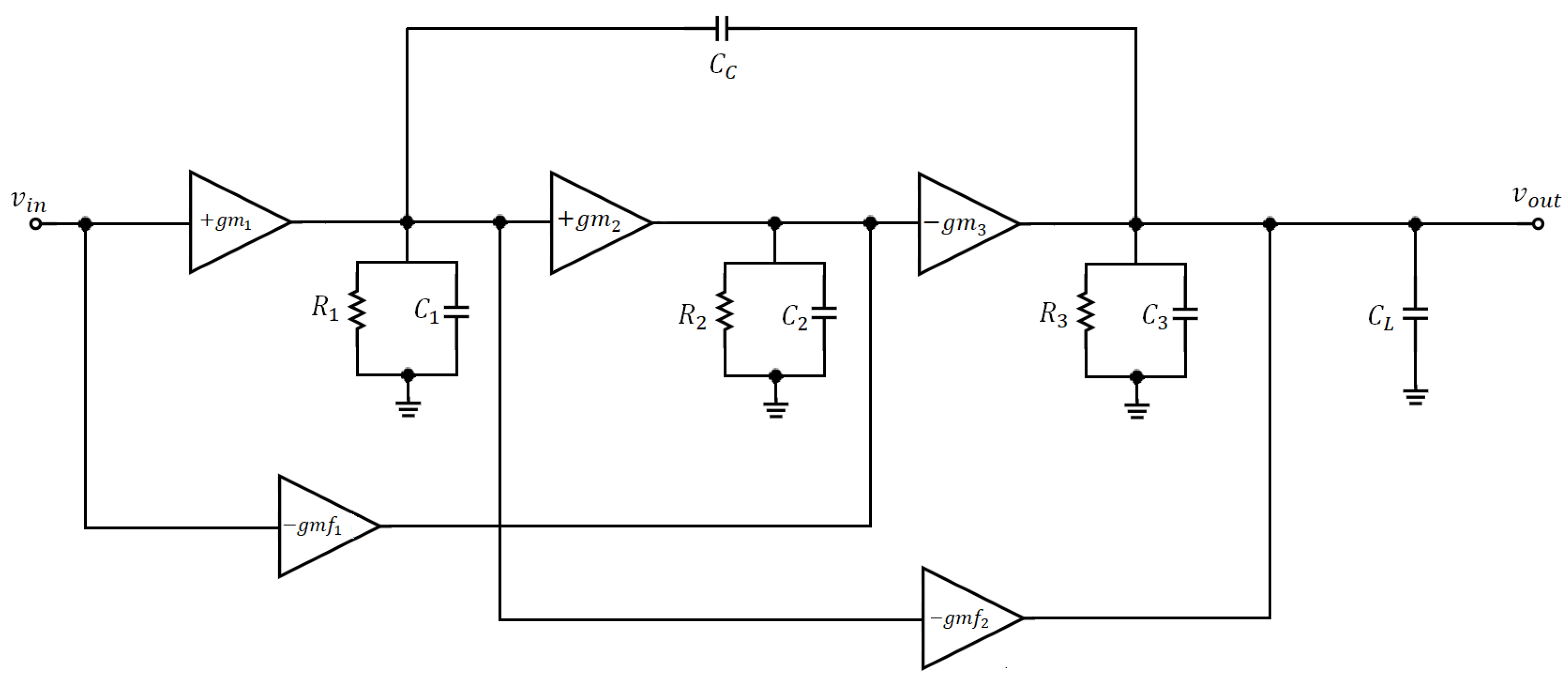
The structure of the proposed three-stage error amplifier (EA) is depicted in Figure 2, where the output resistance and capacitance of each stage are denoted by R 1 3 and C 1 3 , respectively. C c is the compensation capacitor and C L is the load capacitance, which, in this case, is the parasitic capacitance C g s of the pass transistor. The transconductance gain stages g m 1 3 form a three-stage amplifier while the two feed-forward paths are realized by the gain stages g m f 1 and g m f 2 , respectively. The purpose of implementing the feed-forward path from the input of the first stage to the output of the second is to introduce a left-handplane zero in order to improve the stability performance of the structure. The feedback network is realized by the compensation capacitor C c in the Miller architecture, which can be used to place the dominant pole of the system to the desired position but also introduces a right-handplane zero to the system. The main advantage of the proposed architecture is that the left-handplane zero added by the implementation of the feed-forward path g m f 1 to the system should be used to compensate the negative phase shift of the first non-dominant pole. Furthermore, the use of only one compensation capacitor saves valuable chip area while keeping the slew rate performance of the amplifier almost unaffected. The push-pull output and second stage formed by the transconductance and the feed-forward paths g m 2 and g m f 1 , as well as g m 3 and g m f 2 , enhance the transient performance of the proposed amplifier while keeping the power consumption low at steady state.

2.3. Multiloop Amplifier

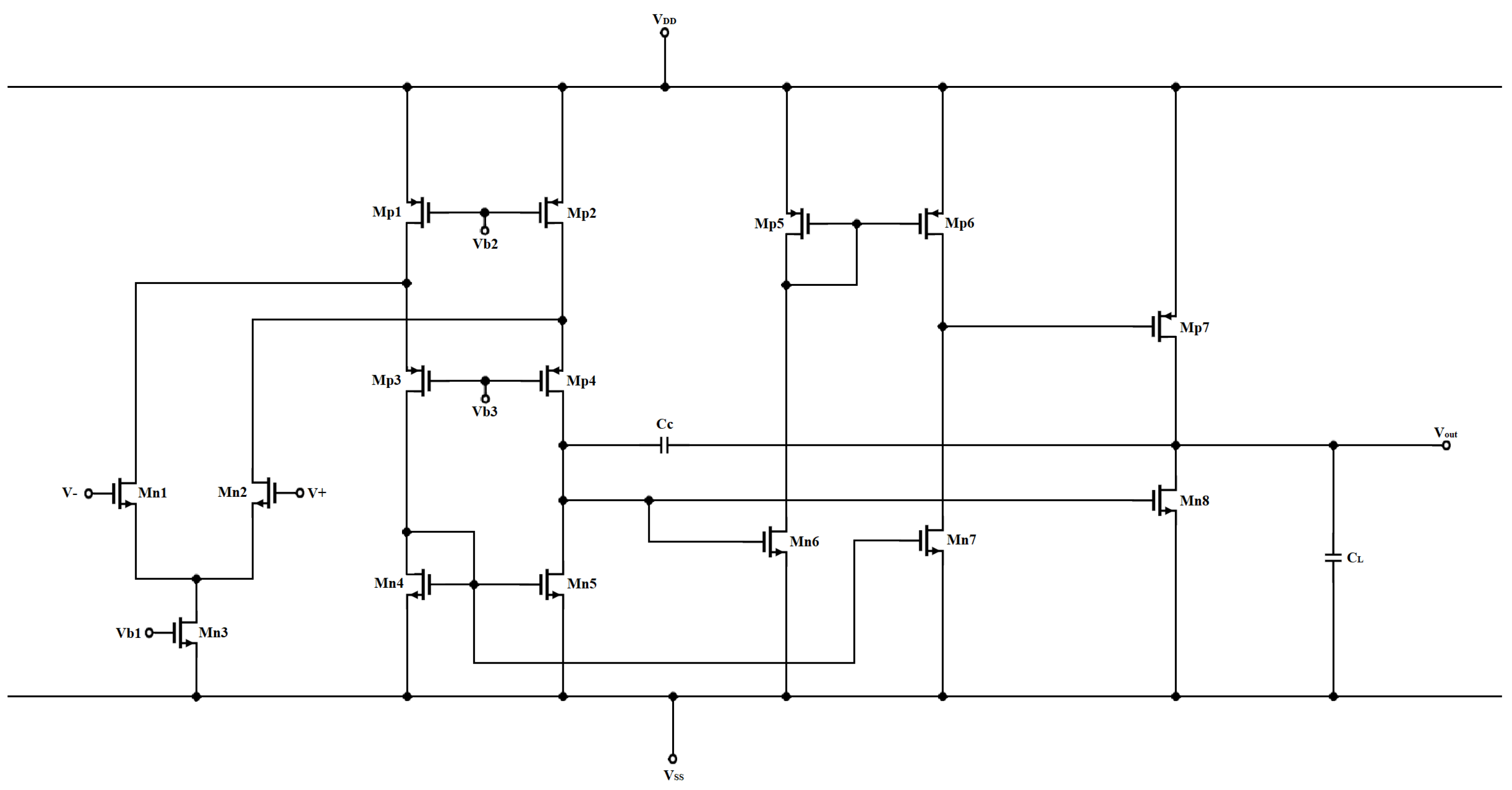
The circuit implementation of the proposed architecture is depicted in Figure 3 and will be described in detail in this sub-section. The first stage of the amplifier is realized by a folded cascode NMOS operational transconductance amplifier OTA. NMOS OTA was preferred over a p-channel metal-oxide semiconductor (PMOS) due to the fact that the power supply voltage is 1 V while the reference voltage is quite high in comparison with the supply voltage at 0.6 V. So, the use of a PMOS OTA is prohibitive because it would be impossible to bias the PMOS current mirror which provides the necessary bias current to the differential pair. It consists of the transistors M n 1 and M n 2 , which comprise a simple differential pair realizing the first transconductance gain g m 1 . The second transconductance stage consists of the transistor M n 6 connected in a simple common source topology along with the PMOS current mirror M p 5 ,   M p 6 , which inverts the phase of the signal, thus making the gain positive. The transistor M n 7 represents the first feed-forward path and it can be easily biased by properly scaling the NMOS current mirror M n 4 ,   M n 5 , as well as the PMOS current mirror M p 5 ,   M p 6 , forming a push-pull stage. Finally the output gain stage is formed by the transistor M p 7 in a common source topology, while the second feed-forward stage g m f 2 is realized by the transistor M n 8 . Yet again, the second feed-forward stage comprises a push-pull output stage, which can be easily biased by sizing properly the current mirror M n 4 ,   M n 5 as well as the transistor M n 8 . The compensation capacitor C c represents the feedback network, which will by used to stabilize the amplifier, while the C L capacitor is the load capacitance of the amplifier, in this case, the parasitic capacitance C g s of the pass transistor. The transistor dimensions are depicted in Table 1.

3. LDO Analysis and Modeling

3.1. Stability Analysis

In this section, an analytical stability analysis will be conducted. The computation of the transfer function is a necessity in order to properly analyze the circuit; the small signal model of the proposed architecture is depicted in Figure 4 [37,38]. Applying the Kirchhoff voltage and current laws leads to the following system of equations in the Laplace frequency domain:
V 1 = g m 1 R 1 V i n + s R 1 C c V o u t 1 + s R 1 ( C c + C 1 )
V 2 = g m 2 R 2 V 2 g m f 1 R 2 V i n 1 + s R 2 C 2
V o u t = g m 3 R 3 V 2 + ( s C c R 3 g m f 2 R 3 ) V 1 1 + s R 3 ( C c + C 3 )
where V i is the AC voltage across the i-node, g m i is the conventional transconductance gain of each stage, R i and C i are the output resistance and capacitance of each stage, while g m f i represents the transconducnce gain of each feed-forward path.
The solution of the above system results in the transfer function of the circuit by taking into consideration the following assumptions: (1) the compensation capacitor C c is much greater than the parasitic capacitor C 1 3 and the load capacitor C L = C g s . (2) the gain of each stage is much greater than 1.
G ( s ) = V o u t V i n = N ( s ) D ( s )
The nominator of the transfer function is
N ( s ) = s 2 C c C 2 R 1 R 2 R 3 g m 1 + s R 1 R 2 R 3 ( g m 3 g m f 1 C c g m 1 g m f 2 C 2 ) A d c
where A d c = g m 1 g m 2 g m 3 R 1 R 2 R 3 . The nominator of the transfer function is a second-degree polynomial function whose roots are the zeros of the system. It is easily understood that there is one positive and one negative root since the constant term of the polynomial is a negative number. So, a right-handplane zero is introduced, which should lie at very high frequencies by properly choosing the value of the transconductance gain g m f 2 , as well as a left-handplane zero, which will cancel the negative phase shift of the first non-dominant pole by tuning the value of the first feed-forward transconductance gain g m f 1 .
The denominator of the transfer function is
D ( s ) = s 3 C c C 1 R 1 R 2 R 3 + s 2 C c C 2 R 1 R 2 R 3 g m f 2 + s C c R 1 R 2 R 3 g m 2 g m 3 + 1
Due to the computational complexity which the transfer function introduces to the analytical computation of the poles, the Open-Circuit Time Constants (OCTC) method is applied [39]. OCTC gives an estimation (usually pessimistic) for the position of the poles of a circuit. The accuracy of this method is sufficient when designing a circuit by providing much simpler equations, especially when dealing with complicated transfer functions. So, by applying this method, the dominant pole is derived as
p 3 d b = 1 C c R 1 R 2 R 3 g m 2 g m 3
which is expected, as it can also be approximated using the first-order coefficient and the constant term of the denominator of the transfer function. In amplifier design, a single-pole approximation is usually desirable in order to achieve both high DC gain, which means high DC PSRR when used as an error amplifier in an LDO, and decent stability performance. The calculation of the unity gain frequency ω t is a necessity when stabilizing an amplifier. In a single-pole approximation, the unity gain frequency can be easily derived as
ω t = A d c p 3 d b = g m 1 C c
From the last result, it is obvious that in order to increase the bandwidth of the amplifier, the first stage should be biased in such a manner as to result in a higher transconductance gain g m 1 or the capacitance of the compensation capacitor should be reduced. The system must have a decent phase margin in order to ensure that it is always stable and robust. The phase margin is given by
ϕ p m = 90 o t a n 1 ( ω t p 3 d b ) t a n 1 ( ω t ω p 1 ) t a n 1 ( ω t ω z 1 ) t a n 1 ( ω t ω p 2 ) t a n 1 ( ω t ω z 2 )
where ω p 1 and ω p 2 represent the non-dominant poles of the system and ω z 1 and ω z 2 are the right- and the left-handplane zeros, respectively. As mentioned above, the frequencies where the second non-dominant pole and the right-handplane zero lie are much higher than the unity gain frequency, so it must be ensured that ω p 1 = ω z 1 in order to achieve the optimal phase margin.

3.2. Noise Analysis

Noise in LDO regulators is a typical parameter that should be taken into consideration when designing. It refers to the thermal and flicker noise of transistors and resistors specified as the output voltage spectral density ( V / Hz ) or as the integrated voltage density ( V r m s ), which is the integration of the output voltage spectral density over a bandwidth [37,38]. The main noise contributors in LDO regulators are S n r e f ( f ) , S n E A ( f ) , S n p a s s ( f ) , S n R ( f ) , which represent the output voltage density of the reference voltage, the error amplifier, the pass transistor and the resistance R of the feedback network, respectively [23]. So, the noise of an LDO regulator is given by
S n ( f ) = S n r e f ( f ) + S n E A ( f ) + S n p a s s ( f ) + S n R ( f )
The noise provided by the error amplifier is typically much higher than the noise of the voltage reference, the pass transistor and the feedback network. So, by taking into consideration this assumption, the noise of the LDO regulator is derived as
S n ( f ) = S n E A ( f )
So, it is essential to analytically calculate the output voltage density of the three-stage proposed error amplifier, which is given by the following equation:
S n E A ( f ) = S n 1 ( f ) + S n 2 ( f ) A v 1 + S n 3 ( f ) A v 1 A v 2
where S n i ( f ) , A v i are the output voltage density and the voltage gain of the i-stage, respectively. So, by assuming that the voltage gain is much greater than 1, the output voltage density of the error amplifier depends only on the noise provided by the first stage.
S n E A ( f ) = S n 1 ( f )
The output spectral density of each component is calculated by the equivalent thermal noise in the input of each transistor v e q 2 , multiplied by the voltage gain A v = ( v o u t / v e q ) 2 . The equivalent thermal noise in the input of each transistor is given by
v e q 2 = 4 K T ( 2 3 g m ) δ f
The first stage consists of a folded cascode differential pair, so the output spectral density is
S n E A ( f ) = 2 S n M n 1 , 2 + ( g m M n 4 , 5 g m M n 1 , 2 ) 2 ( S n M n 4 + S n M n 5 )
S n E A ( f ) = 4 K T 4 3 g m 1 ( 1 + μ p ( W / L ) M n 4 , 5 μ n ( W / L ) M n 1 , 2 ) δ f
where μ p and μ n is the mobility of the holes and electrons, respectively, which is strongly dependent on the temperature. Equation (16) implies that in order to reduce the noise of the LDO regulator, the transconductance gain g m 1 of the first stage should be increased. Furthermore, the W / L ratio of the transistors M n 4 and M n 5 should be the minimum possible as long as the biasing of the first stage remains unaffected.

4. Simulation Results

In this section, the performance of the previous analyzed architecture will be presented. The circuit was simulated in the TSMC 90 nm process. All the simulation results are conducted in the implemented layout shown in Figure 5. The simulation results have been derived from the layout, and they include parasitics related to the resistance (R) and capacitance (C). More specifically, the post-layout simulation results also take into account the effects of the parasitic R&C and the coupling capacitance (CC). Additionally, due to the use of techniques suitable for reducing parasitics and the use of parasitic models in the design, the corresponding schematic results did not deviate from the layout results. The implemented LDO regulator is tested for all processes (TT, FF, SS, FS, SF), voltage (0.8 V, 0.9 V, 1 V) and temperature (−25 °C, 27 °C, 125 °C). During the simulation design process, various problems arose, but in this paper, the two main difficulties will be addressed. While the temperature of the environment is decreasing, the threshold voltage of the transistors Vth is increasing rapidly. So, it is very difficult to bias the pass transistor and the current mirrors in the cold corner variations (−25 °C) of the designer to increase the size of these transistors and consume some valuable chip area, but the area saved by lowering the compensation capacitance is much more optimal. The second main problem for the designer is to properly choose the bias current for the first stage in order to minimize the noise of the circuit while maintaining excellent stability performance. The results of the performance parameters are summarized in Table 2, where the column ‘Typ’ refers to the nominal corner case (TT, V D D = 1 V, 27 °C), while the other two columns, ‘Min’ and ‘Max’, refer to the lowest and highest values of each index as these are evaluated after the simulations. The load condition for the simulation is I l o a d = 200 μA | | C l o a d = 300 pF.
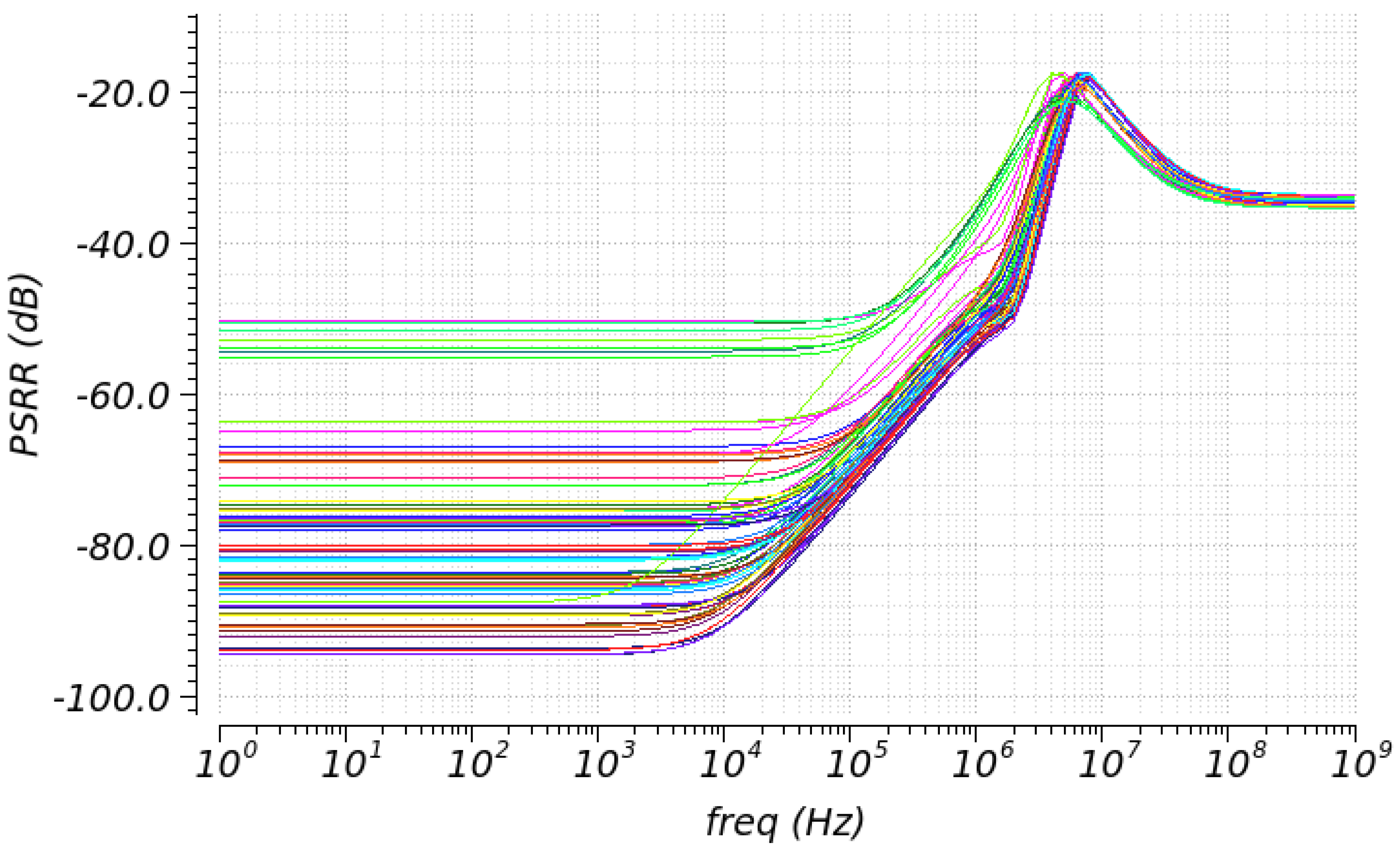
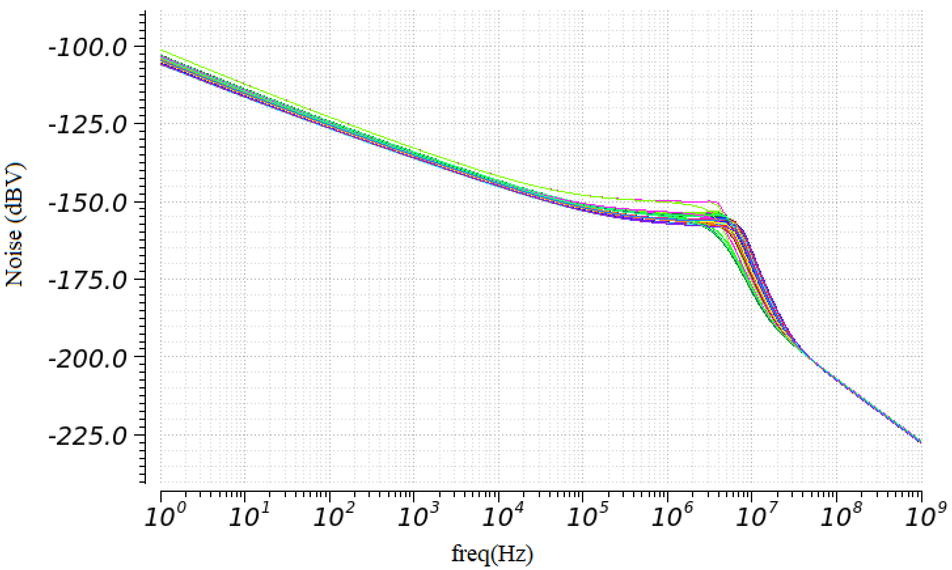
The PSRR response on the various corner cases is depicted in Figure 6. It is quite obvious that, in most cases, the DC PSRR value is quite high (over 80 dB), while the “peak” of the PSRR is always over 18 dB. The main benefit of this implementation is the outstanding stability performance. Based on the measurement results, the LDO regulator is verified to be stable and robust over PVT corner variations with the phase margin always over 75°, while maintaining a relatively high bandwidth due to the fact that the unity gain frequency is over 3 MHz. The trend in the simulations results is that the best performance is achieved in the FF, 125 °C, 1.2 V corner variation, while the worst performance is in the SS, −25 °C, 0.9 V corner variation.The above goals were achieved using an on-chip capacitor with a capacitance of only 2 pF, which saves valuable chip area and highlights the value of the multiloop compensation technique, which improves the spectacular Miller compensation technique. Lastly, Figure 7 depicts the noise response of the LDO regulator, which seems almost unaffected over the PVT corner variations, but is strongly dependent on the compensation.

5. Comparison and Discussion

In this section, the proposed architecture is compared with other related LDO regulators that utilize alternative techniques. In Table 3 and Table 4, the architecture is compared in terms of the typical metrics, which are the necessary variables of merit when designing an LDO. In general, the supply voltage is a critical specification, along with the PSRR metric. The most important metric is the stability of the system, since without it, the system will always be unstable and would not operate properly in all other metrics.
Specifically, the proposed architecture outperforms the other architectures in terms of stability while maintaining a relatively low power consumption (less than 100 μW). The multiloop technique provides a very robust design with high stability metrics (the highest value in terms of the phase margin) without the need for a compensation capacitor of high capacitance and power-hungry design, saving valuable chip area and energy. Despite the fact that the unity gain bandwidth is quite high (around 6 MHz), the stability performance is almost unaffected. Additionally the DC PSRR metric is at very high levels—approximately 85 dB in the nominal case. Lastly, the supply voltage has been dropped down to 1 V, which makes the proposed architecture suitable for low-voltage supply applications.

6. Conclusions

This work introduced an analog integrated low-power multiloop stabilized LDO regulator for low-voltage and low-power applications. It comprises a multiloop error amplifier, a native pass-transistor and a resistor used as a feedback network. The proposed architecture was designed and tested in the TSMC 90 nm CMOS process. Post-layout simulations were conducted, which confirmed the proper operation of the circuit over PVT variations. The architecture proved to be stable and robust over all variations, with a phase margin always over 75°. Valuable chip area was saved by using a compensation capacitor of only 2 pF, which highlights the value of the multiloop compensation technique. It is obvious that various techniques could be developed to further improve the performance of the LDO regulator. In future research, a combination of an LDO regulator along with a BGR circuit which uses the multiloop compensation technique presented in this paper would be possible to be implemented.

Author Contributions

Investigation, K.K. and V.A.; writing—original draft, K.K. and V.A.; writing—review and editing, K.K., V.A., N.U. and P.P.S. All authors have read and agreed to the published version of the manuscript.

Funding

This research received no external funding.

Institutional Review Board Statement

Not applicable.

Informed Consent Statement

Not applicable.

Data Availability Statement

Data are contained within the article.

Conflicts of Interest

The authors declare no conflicts of interest.

References

  1. Kassakian, J.G.; Jahns, T.M. Evolving and emerging applications of power electronics in systems. IEEE J. Emerg. Sel. Top. Power Electron. 2013, 1, 47–58. [Google Scholar] [CrossRef]
  2. Shearer, F. Power Management in Mobile Devices; Elsevier: Amsterdam, The Netherlands, 2011. [Google Scholar]
  3. Katiraei, F.; Iravani, M.R. Power management strategies for a microgrid with multiple distributed generation units. IEEE Trans. Power Syst. 2006, 21, 1821–1831. [Google Scholar] [CrossRef]
  4. Sobhan Bhuiyan, M.A.; Hossain, M.R.; Minhad, K.N.; Haque, F.; Hemel, M.S.K.; Md Dawi, O.; Ibne Reaz, M.B.; Ooi, K.J. CMOS low-dropout voltage regulator design trends: An overview. Electronics 2022, 11, 193. [Google Scholar] [CrossRef]
  5. Chyan, T.Y.; Ramiah, H.; Hatta, S.W.M.; Lai, N.S.; Lim, C.C.; Chen, Y.; Mak, P.I.; Martins, R.P. Evaluation and perspective of analog low-dropout voltage regulators: A review. IEEE Access 2022, 10, 114469–114489. [Google Scholar] [CrossRef]
  6. Lai, L.F.; Ramiah, H.; Tan, Y.C.; Lai, N.S.; Lim, C.C.; Chen, Y.; Mak, P.I.; Martins, R.P. Design Trends and Perspectives of Digital Low Dropout Voltage Regulators for Low Voltage Mobile Applications: A Review. IEEE Access 2023, 11, 85237–85258. [Google Scholar] [CrossRef]
  7. Kularatna, N. Review of Fundamentals Related to DC Power Supply Design and Linear Regulators. In DC Power Supplies; CRC Press: Boca Raton, FL, USA, 2018; p. 1. [Google Scholar]
  8. Hsia, S.C.; Sheu, M.H.; Wu, S.H. Wide operation range high-voltage linear regulator chip design. Electr. Eng. 2024, 106, 2197–2208. [Google Scholar] [CrossRef]
  9. Kampus, V.; Rang, T. A smart capless voltage regulator for very high bandwidth A/D and D/A converters in a standard 28 nm CMOS process. In Proceedings of the 2016 15th Biennial Baltic Electronics Conference (BEC), Tallinn, Estonia, 3–5 October 2016; pp. 43–46. [Google Scholar]
  10. Eleftheriou, N.P.; Ntasiou, O.; Alimisis, V.; Sotiriadis, P.P. A Low-Power Temperature and Process Insensitive CMOS Power Management Unit. In Proceedings of the 2024 Panhellenic Conference on Electronics & Telecommunications (PACET), Thessaloniki, Greece, 28–29 March 2024; pp. 1–4. [Google Scholar]
  11. Carreon-Bautista, S.; Huang, L.; Sanchez-Sinencio, E. An autonomous energy harvesting power management unit with digital regulation for IoT applications. IEEE J. Solid-State Circuits 2016, 51, 1457–1474. [Google Scholar] [CrossRef]
  12. Hu, J.; Ismail, M. CMOS High Efficiency On-Chip Power Management; Springer Science & Business Media: Cham, Switzerland, 2011. [Google Scholar]
  13. Marasco, K. How to successfully apply low-dropout regulators. Analog Dialogue 2009, 43. [Google Scholar]
  14. Torres, J.; El-Nozahi, M.; Amer, A.; Gopalraju, S.; Abdullah, R.; Entesari, K.; Sanchez-Sinencio, E. Low drop-out voltage regulators: Capacitor-less architecture comparison. IEEE Circuits Syst. Mag. 2014, 14, 6–26. [Google Scholar] [CrossRef]
  15. Silva-Martinez, J.; Liu, X.; Zhou, D. Recent advances on linear low-dropout regulators. IEEE Trans. Circuits Syst. II Express Briefs 2020, 68, 568–573. [Google Scholar] [CrossRef]
  16. Haid, J.; Kargl, W.; Leutgeb, T.; Scheiblhofer, D. Power management for RF-powered vs. battery-powered devices. In Proceedings of the Workshop on Wearable and Pervasive Computing, Graz, Austria, 8–9 March 2005. [Google Scholar]
  17. Joshi, K. Mixed-Mode Adaptive Ripple Canceller for Switching Regulators; Arizona State University: Tempe, AZ, USA, 2016. [Google Scholar]
  18. Xiu, Y.; Rosenbaum, E. Analysis and Design of Integrated Voltage Regulators for Supply Noise Rejection During System-Level ESD. IEEE Trans. Circuits Syst. I Regul. Pap. 2020, 67, 4199–4210. [Google Scholar] [CrossRef]
  19. Wang, L. High Performance Distributed On-Chip Voltage Regulation for Modern Integrated Systems; University of South Florida: Tampa, FL, USA, 2018. [Google Scholar]
  20. Li, K. Design and Realization of Low Dropout Voltage Regulators in PMIC for Portable Applications. Ph.D. Thesis, Nanyang Technological University, Singapore, 2020. [Google Scholar]
  21. Choe, Y.J.; Nam, H.; Park, J.D. A Low-Dropout Regulator with PSRR Enhancement through Feed-Forward Ripple Cancellation Technique in 65 nm CMOS Process. Electronics 2020, 9, 146. [Google Scholar] [CrossRef]
  22. Jang, H.J.; Roh, Y.S.; Moon, Y.J.; Park, J.P.; Yoo, C.S. Low drop-out (ldo) voltage regulator with improved power supply rejection. JSTS J. Semicond. Technol. Sci. 2012, 12, 313–319. [Google Scholar] [CrossRef]
  23. Morita, G. Noise Sources in Low Dropout (LDO) Regulators; One Technology Way: Norwood, MA, USA, 2011; pp. 1–12. [Google Scholar]
  24. Teel, J.C. Understanding Noise in Linear Regulators; Texas Instruments Incorporated: Dallas, TX, USA, 2005. [Google Scholar]
  25. Gabriel, A. Rincon-Mora, Member, I.; Phillip E. Allen, Fellow, I. A Low-Voltage, Low Quiescent Current, Low Drop-Out Regulator. IEEE J. Solid-State Circuits 1998, 33, 36–44. [Google Scholar]
  26. Kim, Y.I.; Lee, S.S. A Capacitorless LDO Regulator with Fast Feedback Technique and Low-Quiescent Current Error Amplifier. IEEE Trans. Circuits Syst. 2013, 60, 326–330. [Google Scholar] [CrossRef]
  27. Tan, X.L.; Chong, S.S.; Chan, P.K.; Dasgupta, U. A LDO regulator with weighted current feedback technique for 0.47 nF–10 nF capacitive load. IEEE J. Solid-State Circuits 2014, 49, 2658–2672. [Google Scholar] [CrossRef]
  28. Irianto, S.A.; Prasetyo, W.E.; Dyah, N.; Kurniawan, H.R. A 4 V, 100 MA Low Dropout Voltage Regulator (LDO) for Mobile Phone Solar Charger Application. ICIC Int. 2021, 13, 553. [Google Scholar]
  29. Ziadi, Y.; Qjidaa, H. A High Efficiency Li-Ion Battery LDO-Based Charger for Portable Application. Hindawi Publ. Corp. Act. Passiv. Electron. Compon. 2015, 2015, 591986. [Google Scholar] [CrossRef]
  30. Banba, H.; Shiga, H.; Umezawa, A.; Miyaba, T.; Tanzawa, T.; Atsumi, S.; Sakui, K. A CMOS bandgap reference circuit with sub-1-V operation. IEEE J. Solid-State Circuits 1999, 34, 670–674. [Google Scholar] [CrossRef]
  31. Johns, D.A.; Martin, K. Analog Integrated Circuit Design; John Wiley & Sons: Hoboken, NJ, USA, 2008. [Google Scholar]
  32. Alimisis, V.; Arnaoutoglou, D.G.; Serlis, E.A.; Kamperi, A.; Metaxas, K.; Kyriacou, G.A.; Sotiriadis, P.P. A radar-based system for detection of human fall utilizing analog hardware architectures of decision tree model. IEEE Open J. Circuits Syst. 2024, 5, 224–242. [Google Scholar] [CrossRef]
  33. Khateb, F.; Kulej, T.; Akbari, M.; Steffan, P. 0.3-V bulk-driven nanopower OTA-C integrator in 0.18 μm CMOS. Circuits Syst. Signal Process. 2019, 38, 1333–1341. [Google Scholar] [CrossRef]
  34. Alimisis, V.; Dimas, C.; Pappas, G.; Sotiriadis, P.P. Analog realization of fractional-order skin-electrode model for tetrapolar bio-impedance measurements. Technologies 2020, 8, 61. [Google Scholar] [CrossRef]
  35. Charitos, P.; Alimisis, V.; Eleftheriou, N.P.; Sotiriadis, P.P. A General Purpose 2 MHz 68 μW Temperature Compensated Reference Clock Oscillator. In Proceedings of the 2024 Panhellenic Conference on Electronics & Telecommunications (PACET), Thessaloniki, Greece, 28–29 March 2024; pp. 1–4. [Google Scholar]
  36. Hanson, S.; Sylvester, D. A 0.45–0.7 V sub-microwatt CMOS image sensor for ultra-low power applications. In Proceedings of the 2009 Symposium on VLSI Circuits, Kyoto, Japan, 16–18 June 2009; pp. 176–177. [Google Scholar]
  37. Koniavitis, K.; Alimisis, V.; Eleftheriou, N.P.; Kamperi, A.; Sotiriadis, P.P. A Multistage Nested-Loops Stabilized Operational Amplifier. In Proceedings of the 2024 Panhellenic Conference on Electronics & Telecommunications (PACET), Thessaloniki, Greece, 28–29 March 2024; pp. 1–4. [Google Scholar]
  38. Chong, S.S.; Chan, P.K. Cross feedforward cascode compensation for low-power three-stage amplifier with large capacitive load. IEEE J. Solid-State Circuits 2012, 47, 2227–2234. [Google Scholar] [CrossRef]
  39. Gray, P.R.; Hurst, P.J.; Lewis, S.H.; Meyer, R.G. Analysis and Design of Analog Integrated Circuits; John Wiley & Sons: Hoboken, NJ, USA, 2024. [Google Scholar]
  40. El-Nozahi, M.; Amer, A.; Torres, J.; Entesari, K.; Sánchez-Sinencio, E. High PSR low drop-out regulator with feed-forward ripple cancellation technique. IEEE J. Solid-State Circuits 2010, 45, 565–577. [Google Scholar] [CrossRef]
  41. Lim, Y.; Lee, J.; Park, S.; Jo, Y.; Choi, J. An external capacitorless low-dropout regulator with high PSR at all frequencies from 10 kHz to 1 GHz using an adaptive supply-ripple cancellation technique. IEEE J. Solid-State Circuits 2018, 53, 2675–2685. [Google Scholar] [CrossRef]
  42. Park, C.J.; Onabajo, M.; Silva-Martinez, J. External capacitor-less low drop-out regulator with 25 dB superior power supply rejection in the 0.4–4 MHz range. IEEE J. Solid-State Circuits 2013, 49, 486–501. [Google Scholar] [CrossRef]
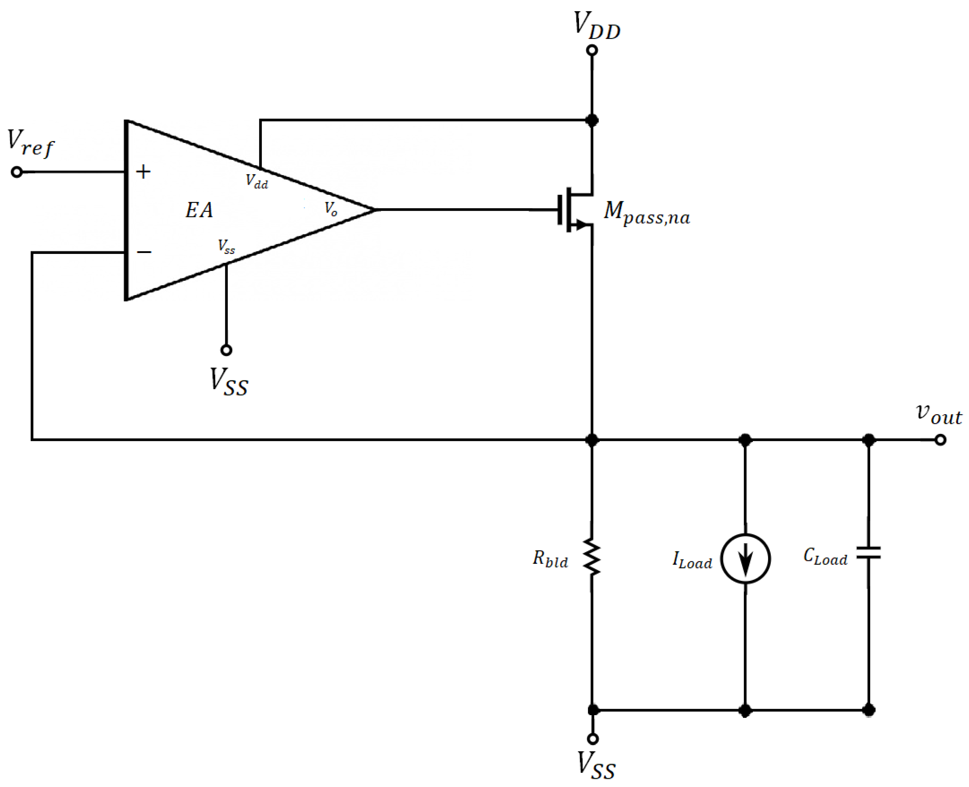
Figure 1. Typical LDO structure.
Electronics 13 03602 g001
Figure 2. Structure of proposed three-stage amplifier.
Electronics 13 03602 g002
Figure 3. Circuit implementation of the proposed three-stage amplifier.
Electronics 13 03602 g003
Figure 4. Small-signal model of the proposed three-stage amplifier.
Electronics 13 03602 g004
Figure 5. Layout of the proposed LDO architecture. The total area is equal to 0.034 mm2. A common-centroid technique is used to address manufacturing considerations.
Electronics 13 03602 g005
Figure 6. PSRRresponse.
Electronics 13 03602 g006
Figure 7. Noiseresponse.
Electronics 13 03602 g007
Table 1. Transistor dimensions.
TransistorW/L ( μ m/ μ m)
M n 1 , M n 2 8 / 0.5
M n 3 19.3 / 1
M n 4 , M n 5 8 / 1
M n 6 , M n 7 0.8 / 1
M n 8 19.2 / 1
M p 1 , M p 2 24 / 1
M p 3 , M p 4 40 / 1
M p 5 , M p 6 2 / 1
M p 7 16 / 1
Table 2. Performance results.
ParameterMinTypMax
Supply voltage (V) 0.9 1 1.1
Regulated output voltage (mV) 599.5 600 600.2
PSRR@DC (dB) 50.36 85.76 94.57
PSRR@100kHz (dB) 49.75 69.94 73.51
PSRR@1MHz (dB) 34.44 51.19 54.18
Worst PSRR (dB) 17.26 18.00 21.41
Output noise@1Hz (dBV/ Hz ) 101.23 104.58 105.99
Output noise@1kHz (dBV/ Hz ) 132.86 135.15 136.25
Output noise@10kHz (dBV/ Hz ) 141.86 144.27 154.33
Output noise@100kHz (dBV/ Hz ) 147.96 151.94 153.08
Output noise@1MHz (dBV/ Hz ) 149.82 155.74 157.17
DC gain (dB) 47.89 82.83 90.98
Phase margin ( ) 75.52 79.90 143.6
Unity gain frequency (MHz) 3.33 6.03 7.77
Table 3. Comparison table.
ProcessSupply VoltageLoad ConditionsDC PSRR
This work90 nm1 V I l o a d = 200 μ A | | C l o a d = 300 pF85 dB
[21]65 nm 1.2 V I l o a d = 20 mA | | R l o a d = 100 Ω 92 dB
[22]130 nm 1.2 V I l o a d = 50 mA | | C l o a d = 4.7 μ F46 dB
[40]130 nm1.15–1.8 V I l o a d = 50 μ A | | C l o a d = 400 pF80 dB
[41]65 nm 1.2 V I l o a d = 100 μ A | | C l o a d = 240 pF70 dB
[42]180 nm 1.8 V I l o a d = 50 mA | | C l o a d = 100 pF62 dB
Table 4. Comparison table. * the stability is affected by the size of the C c capacitor.
Phase MarginUGBWPower ConsumptionEstimated Area
This work79.9°6 MHz95 μ W0.034 mm2
[21]**462 μ W0.092 mm2
[22]**78 μ W0.4 mm2
[40]53° 1.65 MHz32.4 μ W0.049 mm2
[41]40°40 MHz N / A 0.087 mm2
[42]50°1 MHz144 μ W0.14 mm2
Disclaimer/Publisher’s Note: The statements, opinions and data contained in all publications are solely those of the individual author(s) and contributor(s) and not of MDPI and/or the editor(s). MDPI and/or the editor(s) disclaim responsibility for any injury to people or property resulting from any ideas, methods, instructions or products referred to in the content.