Article

High Quality Factor Miniaturized CMOS Transmission Lines Using Cascaded T-Networks for 60 GHz Millimeter Wave Applications

I&E Visionaries Department, Faculty of Information Science and Electrical Engineering, Kyushu University, Fukuoka 819-0395, Japan
*
Author to whom correspondence should be addressed.
Electronics 2024, 13(18), 3748; https://doi.org/10.3390/electronics13183748
Submission received: 8 August 2024 / Revised: 16 September 2024 / Accepted: 18 September 2024 / Published: 20 September 2024
(This article belongs to the Special Issue New Advances in Semiconductor Devices/Circuits)

Abstract

:
This work presents an on-chip 60 GHz lumped element transmission line (TL) using cascaded T-networks with a high Quality factor. Each T-network consists of a series inductance with a shunt capacitance at its center. We have derived the design equations for this TL configuration and proved that a TL whose electrical length ≥ 60° achieves additional miniaturization when implemented with three or more cascaded T-networks. The inductance is implemented using a straight wire model with no ground below it, while the capacitance is implemented using a parallel plate model with a grounding pedestal. Both configurations guarantee maximum inductance per unit length and capacitance per unit area to further improve the miniaturization level. A quarter wavelength TL with three cascaded T-networks is fabricated as proof of concept. The measured and simulated results of the fabricated TL have good agreement, and the measured quality factor is 17 at 60 GHz.

1. Introduction

The implementation of high-performance passive components in complementary metal–oxide–semiconductor (CMOS) technology is vital to optimizing overall chip cost [1,2,3,4,5,6,7,8,9,10,11,12,13,14,15,16,17,18,19,20]. A transmission line (TL) is the core element for many microwave circuits, including Wilkinson power dividers/combiners (WPDCs) [3,4,5,6,7,8], couplers [9], filters [10,11,12,13,14,15,16], and antenna feeding circuits [17,18]. As an example, the WPDC is an essential building block for modern power amplifier (PA) and phased antenna array (PAA) systems. Using WPDCs to combine the output of one or more PAs leads to high output power. Additionally, the PAA systems use the WPDC as the feeding network to achieve a large array factor and correspondingly high gain. In both cases, a compact WPDC is required to guarantee affordable CMOS chip cost. Furthermore, a WPDC with low insertion loss is crucial to avoid losing the original benefit of high gain or high output power. The development of compact and low-loss WPDC depends, mainly, on the quality ( Q ) factor and the level of miniaturization of the TL used.
The electrical length and characteristic impedance of a planar TL are defined by its physical length and width, the height and dielectric constant of the substrate, and the used topology. Recent advancements in materials and fabrication techniques have led to significant improvements in the Q factor and the miniaturization of TLs, which are critical for the performance of various passive components. However, challenges remain in achieving the optimal balance between size, loss, and cost. Miniaturization methods like folding or meandering [9,10,11,12], the slow-wave effect of defected grounds [9,10,11], lumped element loading as capacitance [5], inductance [6,7], combined inductance and capacitance [4], or full replacement with lumped elements [2,3], have been proposed.
In this paper, we propose a new realization of the distributed lumped element TL technique using cascaded T-networks. Previous works have been focused on achieving lower insertion losses without clear insight into the Q factor. Then, compactness was achieved in the component level without insight on the TL miniaturization. Instead, we target achieving a high Q factor with a high level of miniaturization in 0.18 μm CMOS technology. The organization of this paper is as follows: Section 2 describes the theoretical analysis and design of the proposed TL. Section 3 presents the electromagnetic (EM) realization of the proposed TL and the simulation results. Section 4 shows the measurement results in comparison to the simulated results. Finally, Section 5 concludes the paper and describes the possible extensions of this work.

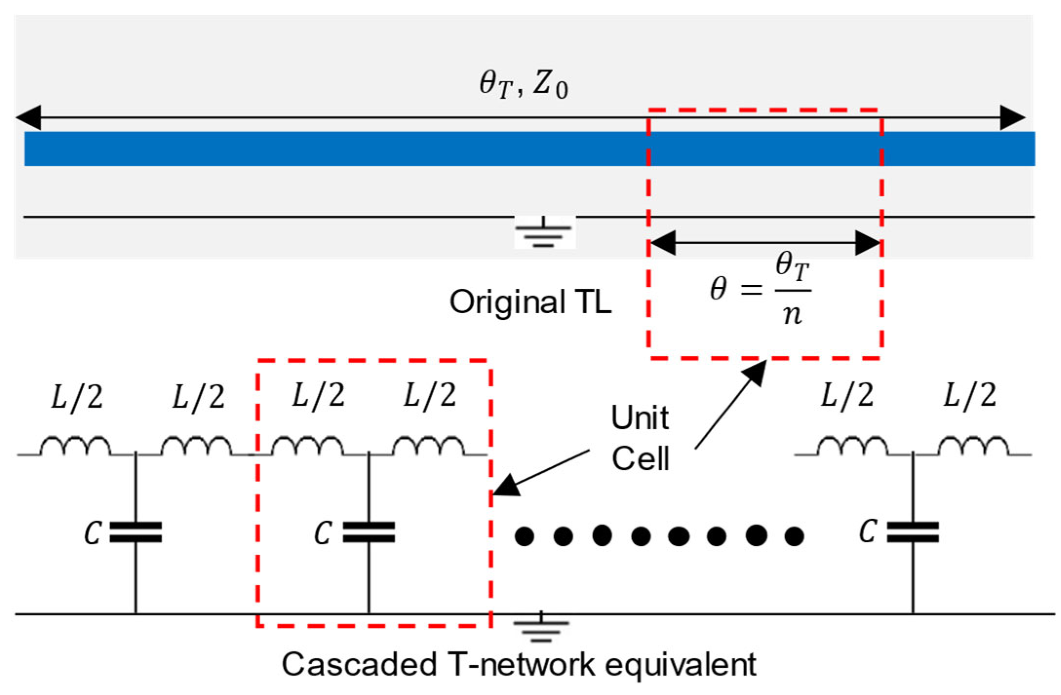
2. Proposed Lumped Element TL Design

2.1. Unit Cell Design

In the lumped element realization technique, the TL is entirely replaced by the π- or T-sections of the lumped inductors and capacitors [2,3,4,5,6,7,8]. Instead, we propose a TL of electrical length, θ T , which is considered as “ n ” cascaded T-network TLs with electrical length θ   as shown in Figure 1.
Each of these is equivalent to a T-network of a series inductor and shunt capacitor. This T-network of the inductor and capacitor should have the same electrical characteristics as the original unit TL, i.e., the electrical length and the characteristic impedance. A unit cell of the original TL and a unit T-network TL, as can be interpreted from Figure 1, are analyzed by equating their ABCD parameter matrices. The ABCD matrix of the TL unit cell with an electrical length, θ , is as follows:
A B C D T L u n i t = cos θ j Z 0 × sin θ j 1 Z 0 × sin θ cos θ
and the T-network has the ABCD matrix as follows:
A B C D T n e t w o r k = 1 ω 2 L C 2 j ω C × 1 ω 2 L C 4 j ω C 1 ω 2 L C 2
Equating the A-terms and C-terms of (1) and (2) allows us to derive the required unit inductance (L) and unit capacitance (C), respectively, as follows:
L = 2 Z 0 ω × tan θ 2
C = 1 ω Z 0 × sin θ

2.2. Optimum Number of Unit T-Networks

Using (3)–(4), we plot Figure 2, which shows the total inductance, L T , and the total capacitance, C T , respectively, versus the number of sections ( n ) for a different θ T , where L T = n × L , C T = n × C , and θ T = n × θ . These calculations are done using Keysight Advanced Design System (ADS) version 2023 update 1. As can be interpreted from Figure 2a, for all the θ T   values, L T decreases as n increases, which allows for the miniaturization of the cascaded T-network TL. Alternatively, as can be interpreted from Figure 2b, for θ T > 60°, C T increases as n increases. Still, a large-valued capacitance with a high Q factor can be easily implemented with a compact size when compared to the inductance implementation. Therefore, we can accept that increased margin in the capacitance.
It is to be noted that both the L T and C T have negligible changes beyond a specific n value depending on the target electrical length of the TL. The reason behind this behavior is that sin θ θ and tan θ / 2 θ / 2 for a small value of θ ; hence, for large n , L and C can be calculated using (5)–(6), respectively. In summary, for θ T > 60°, n should be 3 such that the proposed T-network-based TL achieves the highest miniaturization level for a given θ T .
L Z 0 θ ω
C θ Z 0 ω

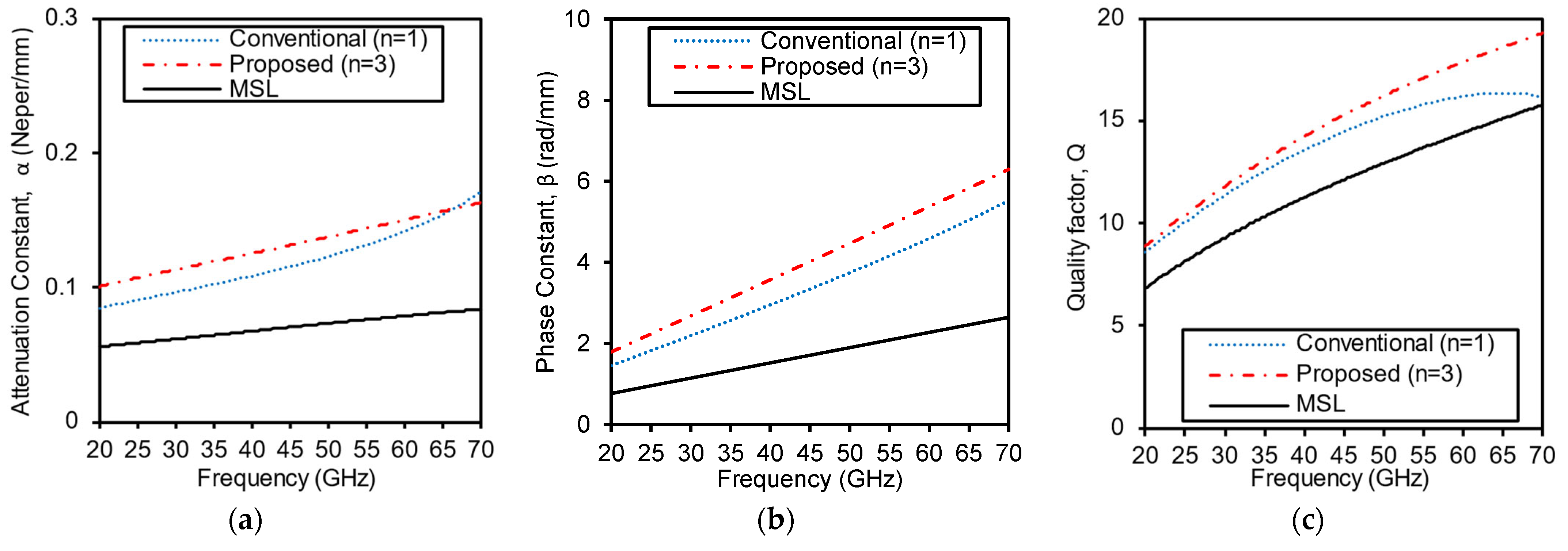
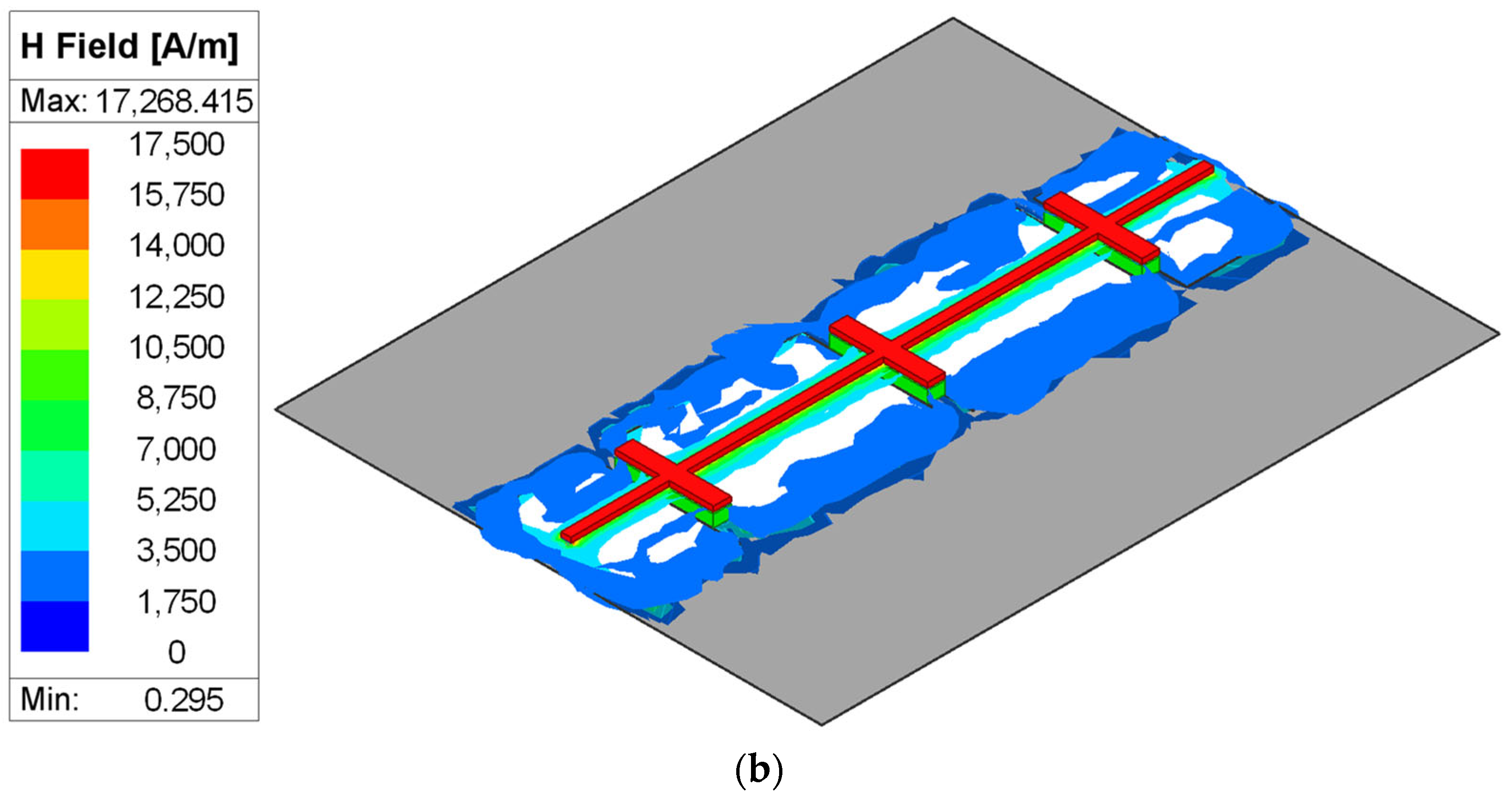
3. EM Model and Simulation Results of a Quarter Wavelength TL

In this section, we design a 50 Ω quarter wavelength TL based on the proposed parameters. The reason for this selection is that the quarter wavelength TL has been widely employed in matching networks, filters, power dividers, and harmonic terminations. The EM model of this design is shown in Figure 3 with three cascaded T-networks (n = 3) for which L = 71.1 pH and C = 26.53 fF, which were calculated using (3) and (4), respectively. EM simulations were carried out using the ANSYS Electronics Desktop version 2023 R1 High-Frequency Structure Simulator (HFSS) package. The EM simulations in HFSS were configured with specific parameters from the vendor design kit to model the TL characteristics accurately, including dielectric constants, substrate height, and conductor dimensions.

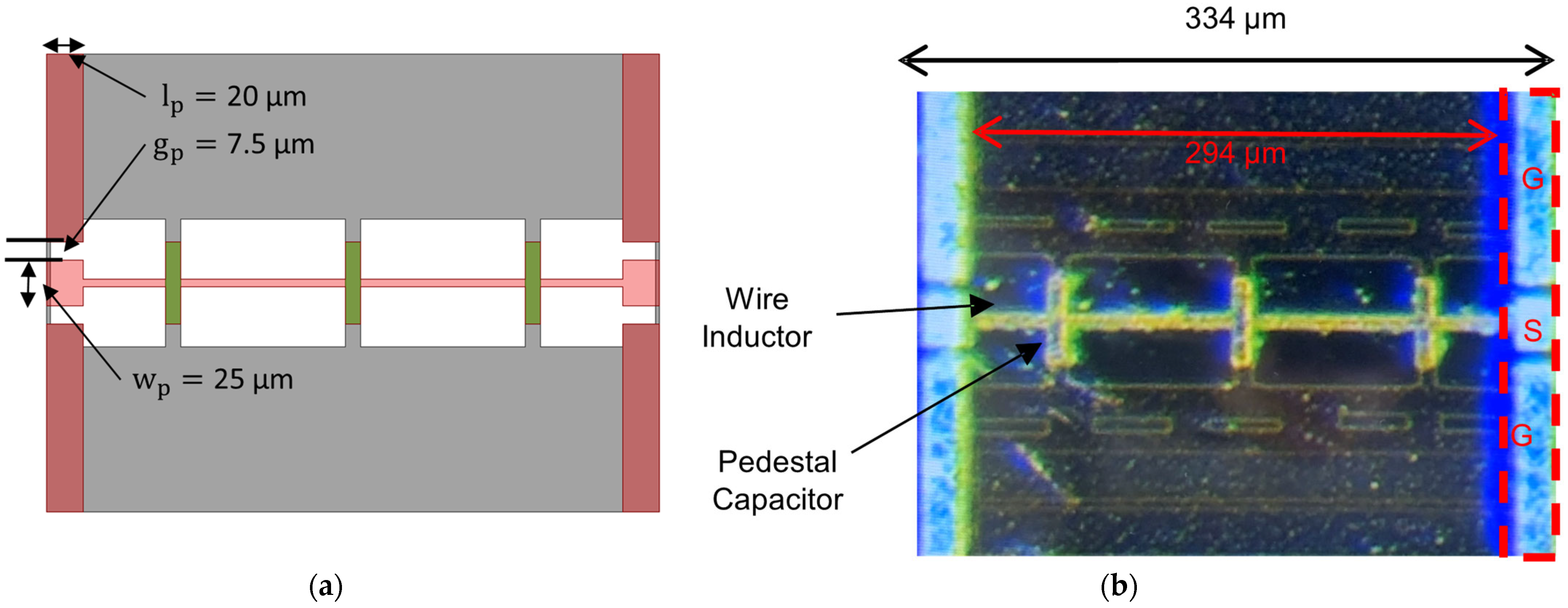
3.1. Practical TL Parameters

The electrical length is calculated as θ T = β l T , where l T is the physical length of the TL and β (rad/mm) is the phase constant at a given frequency. In other words, the physical length of the TL refers to the actual distance that the signal travels, while the electrical length represents the phase shift the signal undergoes as it propagates along the TL at that frequency. Hence, for a given electrical length, maximizing β leads to shorter l T and a higher level of miniaturization.
In this subsection, we discuss the practical realization of TLs. In this context, resistive, dielectric, and radiation losses are inevitable and significantly affect the Q factor. These losses are characterized by the attenuation constant, α (Neper/mm), which represents the rate at which signal power decreases per unit length. The Q factor of a TL is calculated using Equation (7) [21]. Equation (7) shows that the Q factor is inversely related to α, indicating that a higher α results in more energy dissipation and reduced signal fidelity. Minimizing α is essential to reduce noise and maintain signal integrity, as excessive attenuation increases the noise floor, negatively impacting the signal-to-noise ratio (SNR), especially in high-frequency systems.
Q = β 2 × α
In summary, maximizing β and minimizing α are essential for miniaturizing the TL and achieving a high Q   factor. Figure 3 shows the proposed EM model of the quarter wavelength TL, and details on how the elements in Figure 1 are realized in practice are discussed in the following subsections.

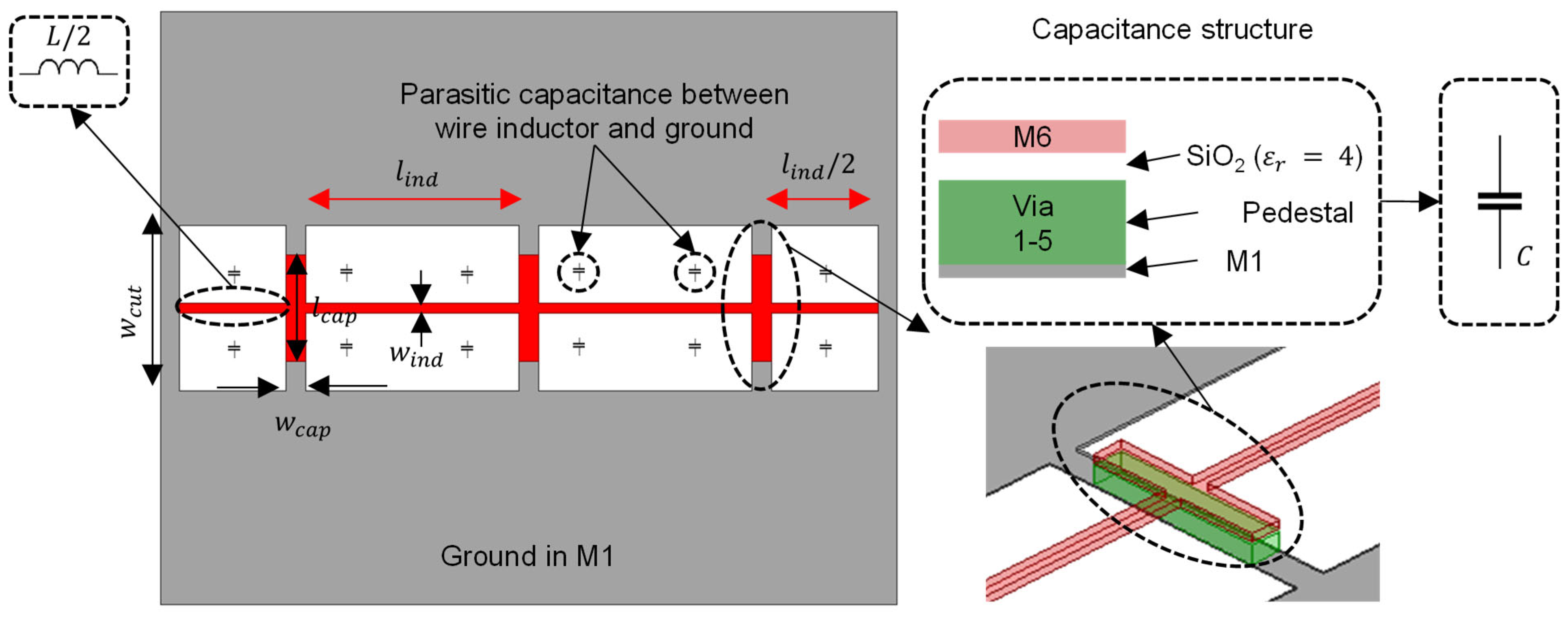
3.2. Unit Capacitance Implementation

The unit capacitance, C , of the proposed quarter wavelength TL is implemented as a parallel plate configuration with a length of l c a p and width of w c a p . A grounding pedestal is formed by combining the metal layers (M1 to M5) for the purpose of increasing the capacitance per unit area; hence, the separation between the capacitor plates is the separation between M5 and M6 ( t 56 ) for which C is calculated as follows:
C = ε r ε 0 l c a p w c a p t 56
where ε r and ε 0 are the relative permittivity of silicon dioxide and the permittivity of air, respectively.

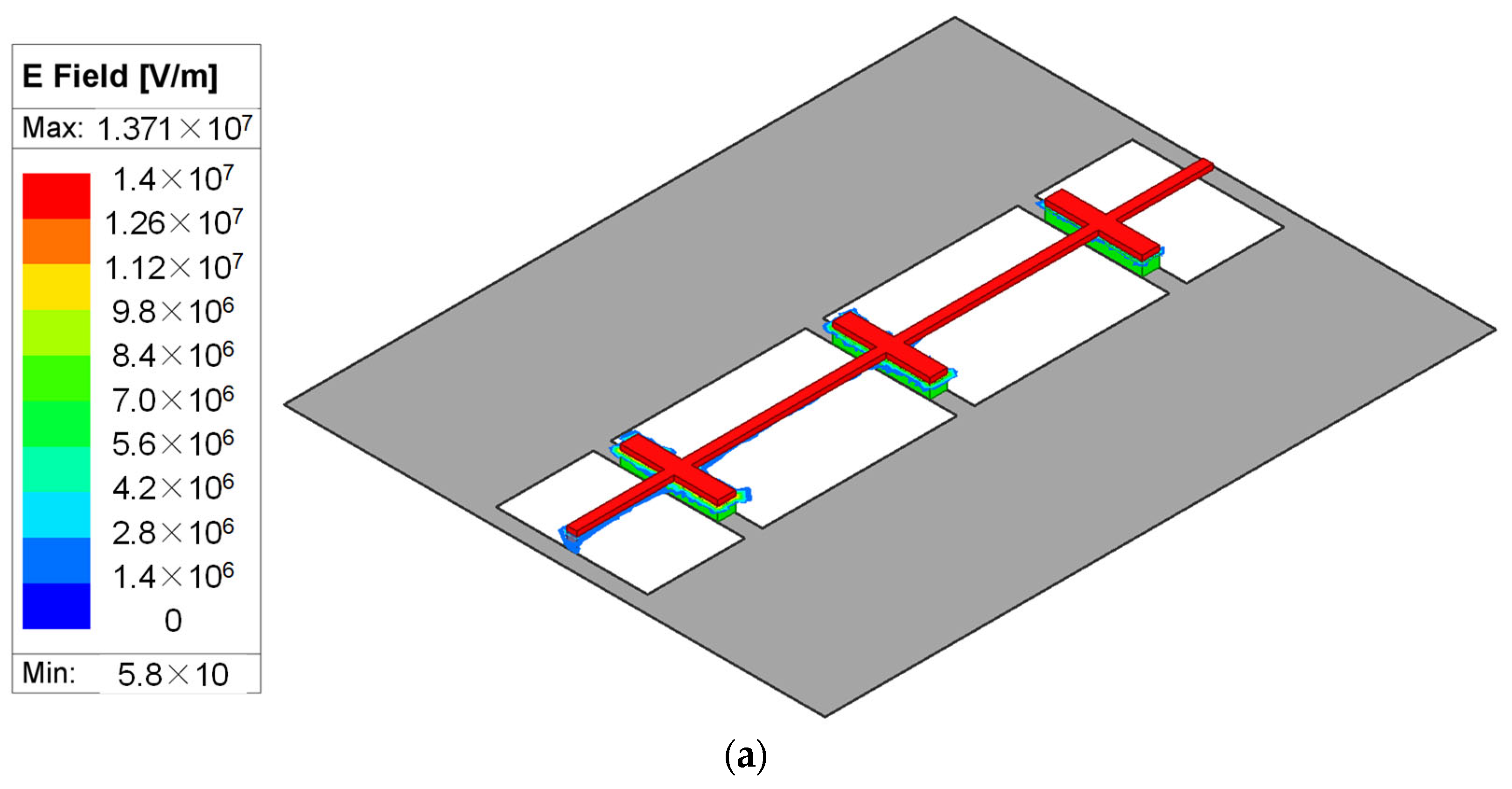
3.3. Unit Inductance Implementation

The unit inductance, L , of the proposed TL is implemented using a straight wire inductance model [22], with a length of l i n d and width of w i n d . We made a cut in the ground plane of a width of w c u t below each straight wire inductance to maximize inductance per unit length. In addition, we selected the lowest metal layer, M1, for implementing the ground to minimize the parasitic capacitance between the ground plane and the wire inductance. In overall, increasing the inductance per unit length leads to a shorter l i n d , i.e., high level of miniaturization.

3.4. Example Designs with Different n T-Networks

In Table 1, we summarize the dimensions of the designs having different numbers of cascaded T-networks of the proposed quarter wavelength TL. The miniaturization ratio in Table 1 is calculated with respect to a reference 50 Ω quarter wavelength microstrip line (MSL) with a length of 700 μm and a width of 12 µm in the same technology. The extraction procedure of these TL propagation parameters ( α and β ) from the Scattering (S) parameters is detailed in [23]. Then, Q factor is calculated using Equation (7). Additionally, a figure-of-merit ( F o M = Q / l T ) is suggested to compare between the different cases. This FoM combines the Q factor that represents the loss performance and the length, l T , that represents the miniaturization level. When n = 3, the best result was achieved. Beyond n = 4, the F o M degrades as more capacitors are used and w c a p contributes more to the overall length.
Furthermore, we compare α , β , and the Q factor of two of these designs (n = 1 “conventional” and 3 “proposed”) with the reference MSL across a wide range frequency in Figure 4a–c, respectively. These designs and the reference MSL have different α and β . But the proposed design (n = 3) has the best Q factor at 60 GHz. This Q factor is higher than both the reference MSL and the conventional design (n = 1). Hence, the proposed realization of the cascaded T-network TL further improves the miniaturization level and the Q factor when compared to conventional lumped element design.
Moreover, the electric (E) and magnetic (H) field distributions of the proposed TL are shown in Figure 5a,b to further clarify its performance. The E-field is mainly concentrated between the capacitor plates as shown in Figure 5a. Also, the H-field is mainly concentrated around the inductive wires with minimal concentration in the defects of ground planes. So, other circuits may be placed nearby, i.e., the area can be reused to maximize the utilization of the chip area.

4. Measurements

We chose the design with n = 3 for the fabrication as it has the largest miniaturization ratio and Q factor as it can be interpreted from Table 1 in the previous section. We used a 180 nm CMOS technology for this fabrication. Figure 6a shows the final EM simulation model after the ground-Signal-Ground (GSG) measurement pads are included. The Cadence IC6.18 Virtuoso tool was used for the CMOS chip layout, adhering to design rules and target specifications optimized for high Q factor and compactness.

4.1. Measurement Setup

The measurement setup consisted of a Keysight Vector Network Analyzer (PNA Series, Part Number: E8361C), which allows for characterization of up to 67 GHz. In addition to the PNA, the measurement setup included a manual probe station, two cables, two Cascade Microtech 100 μm pitch Infinity probes, and a Cascade Microtech impedance standard substrate (Part Number: 101-109) for short-open-load-through calibration. The calibrations were meticulously performed to ensure accuracy in the S-parameter measurements. During the measurements, the samples were placed on the manual probe station, and the infinity probes were precisely aligned using an optical microscope. The Vector Network Analyzer was used to measure S-parameters, and data were collected over a frequency range extending up to 67 GHz. Data analysis involved extracting the attenuation constant, α , the phase-shift constant, β , and the corresponding Q factor using ADS, and comparing them to simulation results to validate the fabricated design.

4.2. Measurement Results

Figure 6b shows the fabricated chip photograph. The pad length, width, and gap are denoted l p , w p , and g p , respectively. The pad dimensions selected for a 50 Ω operation, and their values are as shown in Figure 6a. The measured and simulated α , β , and Q factor have good agreements as shown in Figure 7a–c, respectively, which confirms the operation of the fabricated TL. This TL length is 294 μm (334 μm including pads). It should be noted that the shown measured results are the averaged results of 40 chips.
Figure 6b shows the fabricated chip photograph. The pad length, width, and gap are denoted as l p , w p , and g p , respectively. The pad dimensions selected for a 50 Ω operation, and their values are as shown in Figure 6a. The measured and simulated α , β , and Q factor have good agreements as shown in Figure 7a–c, respectively, which confirms the operation of the fabricated TL. This TL length is 294 μm (334 μm including pads). It is to be noted that these measured results are the averaged results of 40 chips.

4.3. Results Discussion

The measurement results confirm the effectiveness of the proposed cascaded T-network design method for miniaturizing TL while maintaining high performance, as reflected in the agreement between the measured and simulated results. The measured α, β, and Q factor results show strong agreement with the EM simulation results, indicating that the design accurately translates from simulation to actual realization. Specifically, the fabricated TL achieved a physical length of 294 µm (334 µm with pads), demonstrating a 58% reduction compared to a conventional 50 Ω quarter wavelength microstrip line, which typically measures around 700 µm. The averaged results from 40 chips reinforce the consistency and reliability of the fabrication process. The high measured Q factor of 17 at 60 GHz, along with the corresponding attenuation and phase constants (α, β), verifies the success of the design in meeting the performance targets. The slight discrepancies between the measured and simulated values can be attributed to parasites introduced by the measurement pads and process variations inherent in CMOS technology, but these are within the acceptable limits for practical applications.
The performance metrics achieved, particularly the high Q factor and miniaturized size, underscore the feasibility of this design for millimeter wave applications. By minimizing α and maximizing β, the proposed TL not only maintains signal integrity but also achieves substantial miniaturization. This level of performance is crucial for integrating compact, high-efficiency passive components in modern CMOS-based systems, paving the way for advanced RF and microwave circuit designs. Overall, the results validate the proposed method and suggest promising potential for further applications, such as in Wilkinson power dividers and combiners.

5. Conclusions

Conventional lumped element TL realization uses a single T- or π-network with the same electrical characteristics. Instead, in this work, we investigated the realization of lumped element TL using cascaded T-networks and derived the design equation. We found that, for electrical lengths < 60°, any number of cascaded T-networks can achieve a similar miniaturization level. On the contrary, for electrical lengths > 60°, the use of a number of T-networks ≥3 provides a better level of miniaturization and even higher Q factor. Furthermore, we used a straight wire inductance with a defected ground below it to reach the highest inductance per unit length. A 50 Ω quarter wavelength model was fabricated in 0.18 CMOS technology using the proposed method with three cascaded T-networks. The overall length excluding pads was 294 µm, which is 58% shorter than a conventional 50 Ω quarter wavelength microstrip line of 700 µm length. Achieving such a miniaturization level with a high Q factor of 17 at 60 GHz opens the door for realizing compact on-chip passive components in CMOS technology. This may include the utilization of the proposed TL in implementing Wilkinson power divider/combiners with compact size and low loss.

Author Contributions

Conceptualization, A.B. and R.K.P.; methodology, A.B.; software, A.B.; validation, A.B.; formal analysis, A.B.; investigation, A.B.; resources, R.K.P.; data curation, A.B.; writing—original draft preparation, A.B.; writing—review and editing, A.B. and R.K.P.; visualization, A.B.; funding acquisition, R.K.P.; supervision, A.B. and R.K.P. All authors have read and agreed to the published version of the manuscript.

Funding

This work is supported in part by the Very Large Scale Integration (VLSI) Design and Education Center (VDEC), The University of Tokyo in collaboration with Cadence, Keysight, and Mentor Graphic Corporations.

Data Availability Statement

Data are contained within the article.

Acknowledgments

The authors would like to present their deep appreciation to H. Kanaya of the Faculty of Information Science and Electrical Engineering, Kyushu University, Japan, for his persistent support during the measurements.

Conflicts of Interest

The authors declare no conflicts of interest.

References

  1. Pakasiri, C.; Xu, J.-L.; Wang, S. A 10 GHz Compact Balun with Common Inductor on CMOS Process. Electronics 2023, 12, 468. [Google Scholar] [CrossRef]
  2. Ahn, H.-R. Chapter 3.3.5 Conventional Lumped-Element Ring Hybrids. In Asymmetric Passive Components in Microwave Integrated Circuits; John Wiley & Sons: Hoboken, NJ, USA, 2006. [Google Scholar]
  3. Byeon, C.W.; Park, C.S. Low-Loss Compact Millimeter-Wave Power Divider/Combiner for Phased Array Systems. IEEE Microw. Wirel. Compon. Lett. 2019, 29, 312–314. [Google Scholar] [CrossRef]
  4. Abdel Hameed, A.S.; Barakat, A.; Abdel-Rahman, A.B.; Allam, A.; Pokharel, R.K. Design of Low-Loss Coplanar Transmission Lines Using Distributed Loading for Millimeter-Wave Power Divider/Combiner Applications in 0.18-μm CMOS Technology. IEEE Trans. Microw. Theory Tech. 2018, 66, 5221–5229. [Google Scholar] [CrossRef]
  5. Park, S.; Hong, S. Miniaturized Stepped Impedance Transmission Lines for D-Band Wideband Power Divider with Isolation Capacitor. IEEE Solid-State Circuits Lett. 2024, 7, 78–81. [Google Scholar] [CrossRef]
  6. Hettak, K.; Verver, C.J.; Stubbs, M.G.; Morin, G.A. A novel compact uniplanar MMIC Wilkinson power divider with ACPS series stubs. In Proceedings of the IEEE MTT-S International Microwave Symposium, Philadelphia, PA, USA, 8–13 June 2003; pp. 59–62. [Google Scholar]
  7. Elsbury, M.M.; Dresselhaus, P.D.; Benz, S.P.; Popovic, Z. Broadband Lumped-Element Integrated N-way Power Dividers for Voltage Standards. IEEE Trans. Microw. Theory Tech. 2009, 57, 2055–2063. [Google Scholar] [CrossRef]
  8. Zhang, T.; Che, W.; Chen, H. Miniaturized Multiway Unequal Power Divider with Controllable Characteristic Impedances. IEEE Microw. Wirel. Compon. Lett. 2017, 27, 1062–1064. [Google Scholar] [CrossRef]
  9. Lin, Y.-S.; Lan, K.-S.; Chen, B.-S. Wideband Millimeter-Wave Power Divider and SPDT Switch Using Inverting Spiral-Coupled-Line. IEEE Trans. Circuits Syst. II Express Briefs 2023, 70, 1575–1579. [Google Scholar] [CrossRef]
  10. Park, S.; Hong, S. Millimeter-Wave Wideband Differential Four-Way Wilkinson Power Divider with 90° Rotational Symmetric Layout. IEEE Microw. Wirel. Compon. Lett. 2022, 32, 1163–1166. [Google Scholar] [CrossRef]
  11. Chirala, M.K.; Floyd, B.A. Millimeter-wave Lange and ring-hybrid couplers in a silicon technology for E-band applications. In Proceedings of the 2006 IEEE MTT-S International Microwave Symposium Digest, San Francisco, CA, USA, 11–16 June 2006; pp. 1547–1550. [Google Scholar]
  12. Elsaidy, E.; Barakat, A.; Abdel-Rahman, A.B.; Allam, A.; Pokharel, R.K. Ultracompact CMOS 60-GHz Tapped-Line Combline BPF with Two Transmission Zeros Using Defected Ground Structures. IEEE Trans. Compon. Packag. Manuf. Technol. 2018, 8, 1642–1649. [Google Scholar] [CrossRef]
  13. Mahmoud, N.; Barakat, A.; Abdel-Rahman, A.B.; Allam, A.; Pokharel, R.K. Compact Size On-Chip 60 GHz H-Shaped Resonator BPF. IEEE Microw. Compon. Lett. 2016, 26, 681–683. [Google Scholar] [CrossRef]
  14. Barakat, A.; Pokharel, R.; Kaho, T. 60 GHz on-chip mixed coupled BPF with H-shaped defected ground structures. Electron. Lett. 2016, 52, 533–535. [Google Scholar] [CrossRef]
  15. Xiao, Y.; Shan, P.; Zhao, Y.; Sun, H.; Yang, F. Design of a W-Band GaAs-Based SIW Chip Filter Using Higher Order Mode Resonances. IEEE Microw. Wirel. Compon. Lett. 2019, 29, 104–106. [Google Scholar] [CrossRef]
  16. Barakat, A.; Pokharel, R.K. Low-Pass Filtering Admittance Inverter for High Out-of-Band Rejection Millimeter-Wave On-Chip BPF. IEEE Trans. Circuits Syst. II Express Briefs 2023, 70, 3963–3967. [Google Scholar] [CrossRef]
  17. Parisi, A.; Papotto, G.; Ragonese, E.; Palmisano, G. A 1-V 7th-Order SC Low-Pass Filter for 77-GHz Automotive Radar in 28-nm FD-SOI CMOS. Electronics 2021, 10, 1466. [Google Scholar] [CrossRef]
  18. Men, K.; Liu, H.; Yeo, K.S. Design of a Ka-Band U-Shaped Bandpass Filter with 20-GHz Bandwidth in 0.13-μm BiCMOS Technology. Electronics 2020, 9, 1608. [Google Scholar] [CrossRef]
  19. Paudel, B.; Li, X.J.; Seet, B.-C. Design and Modeling of a Terahertz Transceiver for Intra- and Inter-Chip Communications in Wireless Network-on-Chip Architectures. Sensors 2024, 24, 3220. [Google Scholar] [CrossRef] [PubMed]
  20. Chung, M.-A.; Huang, S.-R.; Huang, P.-R. Designed on 0.18 μm CMOS Process Small Size Broadband Millimeter Wave Chip Antenna. Inventions 2023, 8, 64. [Google Scholar] [CrossRef]
  21. Vendelin, G.D.; Pavio, A.M.; Rohde, U.L. Chapter 1.3 Transmission Lines. In Microwave Circuit Design; Wiley: New York, NY, USA, 1990. [Google Scholar]
  22. Grover, F.W. Inductance Calculations: Working Formulas and Tables; Courier Corporation: New York, NY, USA, 2004. [Google Scholar]
  23. Eisenstadt, W.R.; Eo, Y. S-parameter-based IC interconnect transmission line characterization. IEEE Trans. Compon. Hybrids Manuf. Technol. 1992, 15, 483–490. [Google Scholar] [CrossRef]
Figure 1. TL of an electrical length ( θ T ) and characteristic impedance ( Z 0 ) with its equivalent representation as n-cells cascaded T-networks TL model.
Electronics 13 03748 g001
Figure 2. Calculated Equivalent T-network elements for a 50 Ω TL at 60 GHz for different θ T values using (3) and (4). (a) Total inductance ( L T = n L ). (b) Total capacitance ( C T = n C ).
Electronics 13 03748 g002
Figure 3. EM model of the quarter wavelength 50 Ω TL with three T-sections.
Electronics 13 03748 g003
Figure 4. EM simulated performance comparison between MSL, conventional lumped model, and proposed cascaded lumped model. (a) Attenuation Constant. (b) Phase Shift Constant. (c) Quality factor.
Electronics 13 03748 g004
Figure 5. EM simulated field distribution of the proposed cascaded lumped model TL. (a) E-field. (b) H-field.
Electronics 13 03748 g005aElectronics 13 03748 g005b
Figure 6. Layout and fabrication of the proposed TL. (a) EM model of the final layout including measurement pads. (b) Fabricated chip photo.
Electronics 13 03748 g006
Figure 7. Comparison between measured and EM simulated TL characterized performance. (a) Attenuation Constant. (b) Phase Shift Constant. (c) Quality factor.
Electronics 13 03748 g007
Table 1. Optimized dimensions in μm of the Proposed TL.
Line TypenQ
@ 60 GHz
Total   Length   ( l T )   = n × ( w c a p + l i n d )
(Miniaturization Ratio)
l c a p w c a p l i n d w i n d w c u t F o M (mm−1)
@ 60 GHz
MicrostripN/A14.4700 (N/A)N/A20.6
Proposed cascaded T-networks116.2344 (50.8%)9083364.57047.1
218306 (56.3%)63.581454.57058.8
317.9294 (58%)458904.57060.9
417.9294 (58%)34.5865.54.57060.9
517.8300 (57.15%)27.58524.57059.3
617.4300 (57.15%)238424.57058
F o M = Q / l T , l T is the total length in mm.
Disclaimer/Publisher’s Note: The statements, opinions and data contained in all publications are solely those of the individual author(s) and contributor(s) and not of MDPI and/or the editor(s). MDPI and/or the editor(s) disclaim responsibility for any injury to people or property resulting from any ideas, methods, instructions or products referred to in the content.

