Abstract
In the context of locomotive traction systems, the power electronic traction transformer (PETT) represents a pivotal component, fulfilling essential functions pertaining to electrical isolation and power control. The majority of existing PETT prototypes employ a combination of a cascade structure and an ISOP structure. The aforementioned scheme effectively reduces the voltage withstand level of the power devices on the input side, yet it also necessitates the utilisation of a greater number of power devices and passive components within the PETT. In order to further reduce the number of power devices used, this paper proposes a new cascaded PETT design. The proposed PETT will adopt a scheme combining a cascade structure and a hardware circuit multiplexing. This paper first analyses the operation principle of the new circuit under non-single frequency PWM control. It then derives the design equations for some hardware parameters and control circuits. Finally, it verifies the effectiveness of the proposed PETT through simulation analysis.
1. Introduction
The power electronic traction transformer (PETT) is regarded as a potential alternative to conventional transformers in locomotive traction systems, offering a number of advantages [1]. These include a reduction in weight and size, enhanced efficiency, and a lower injection of current harmonics into the grid. In 2012, the world’s inaugural PETT for locomotives was developed and deployed by ABB in conjunction with Swiss Federal Railways [2,3]. This was followed by a series of comprehensive investigations into the potential of PETT, involving numerous research organisations worldwide, such as ABB [4,5,6], Alstom [7], Bombardier [8], Siemens [9], etc. These studies led to the development of PETT prototypes and proof-of-concept machines in various forms.
The cascaded PETT has become a typical circuit structure for PETT design [10,11,12,13,14,15,16], and a detailed illustration of the specific circuit topology can be found in Figure 1. The PETT illustrated in Figure 1 can be regarded as a combination of a cascaded multilevel AC/DC converter and an isolated DC/DC converter. The input side of the AC/DC converter is connected to the AC traction grid, whereby the AC input is converted into a medium-voltage DC voltage. The DC/DC converter achieves electrical isolation while increasing the frequency of the transformer’s transmission voltage, which will result in a significant reduction in the size and weight of the on-board transformer. Furthermore, the incorporation of controllable power devices enhances the intelligence of the locomotive.
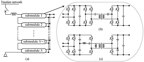
Figure 1.
Typical circuit structure of PETT. (a) PETT circuit. (b) Bombardier. (c) ABB.
As the AC/DC converter is directly linked to the traction network (15 kV/16.7 Hz), the objective is to limit the number of switching devices and reduce the voltage withstand level of these components. In order to achieve this, it is necessary to utilise a CHB structure with 6.5 kV IGBT modules. In order to further reduce the losses in the circuit, the DC/DC converter can be designed as a resonant converter [17,18,19,20,21]. The resonant cavity, which encompasses L-type, LC-type, and LLC-type configurations, guarantees the zero-current and zero-voltage conduction of the power devices within the DC/DC converter.
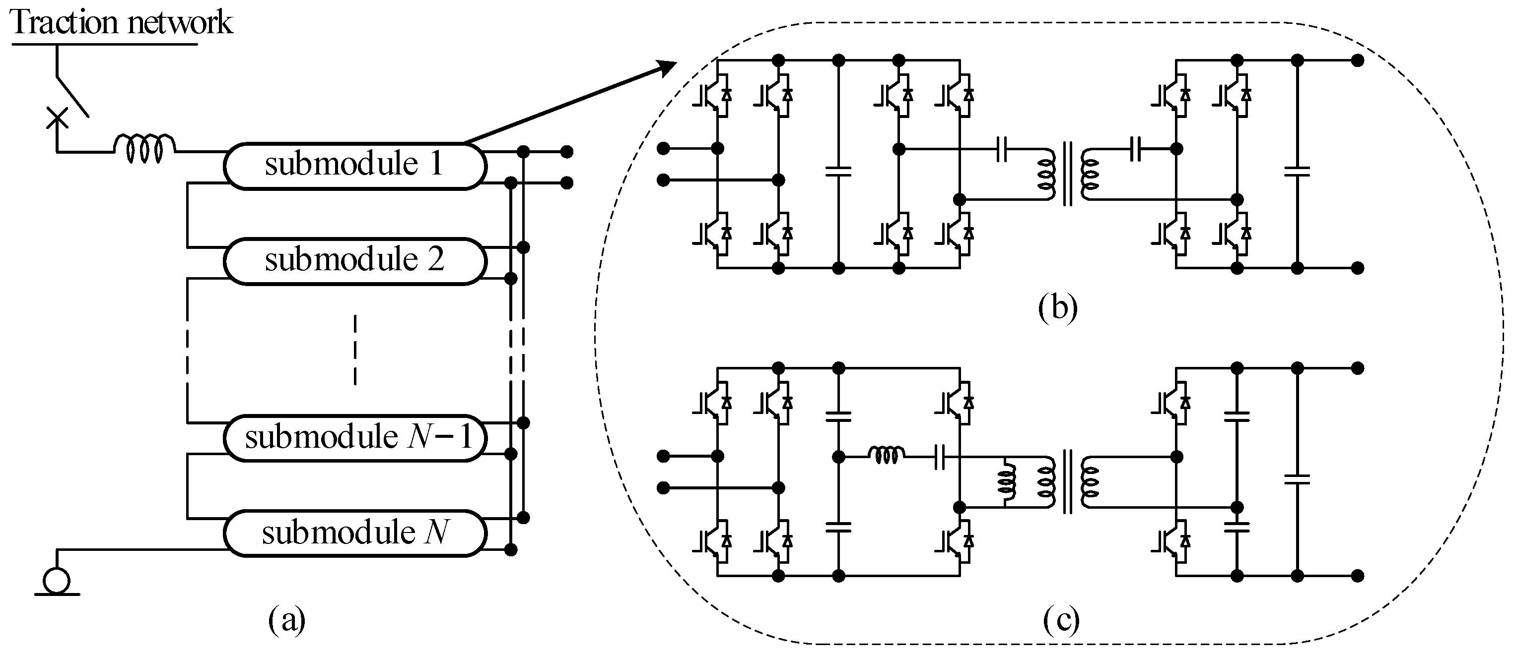
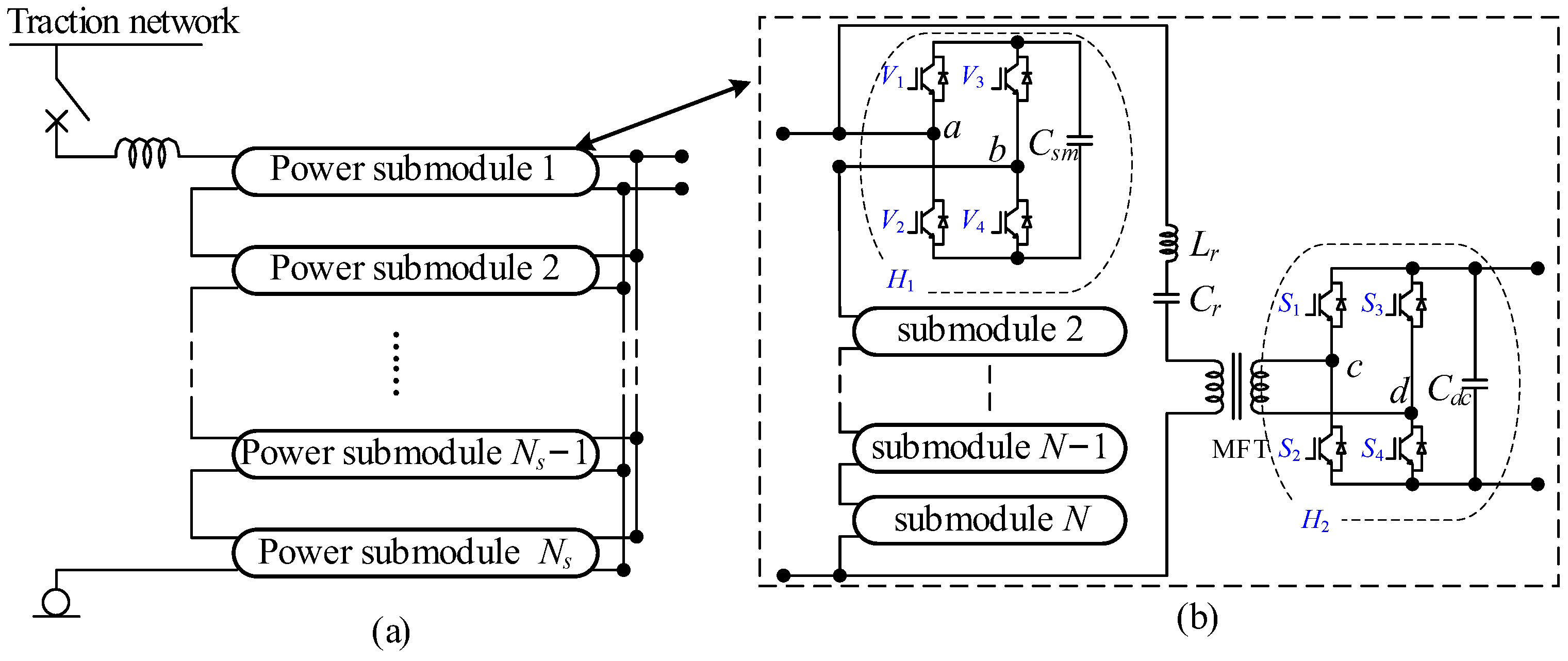
In order to further reduce the number of power devices employed, a novel PETT is designed in this paper, and the specific circuit structure is shown in Figure 2. In the proposed PETT, the number of power units is Ns. The PETT has the following characteristics:
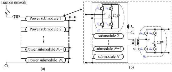
Figure 2.
The proposed PETT circuit. (a) The PETT circuit. (b) The internal circuit of a power unit.
- (i)
- Each power unit is an AC/DC converter and contains a medium-frequency transformer (MFT). The principal aspect of the MFT is constituted by a series of cascaded H-bridge modules, which function as alternating current AC/DC converters. The number of H-bridge modules in this configuration is designated as N. On the secondary side of the MFT, one H-bridge module is employed as an AC/DC converter.
- (ii)
- The two power units collectively constitute a unit group, and there is a distinction between the control signals of these two power units, which will be elucidated subsequently.
- (iii)
- With regard to feature 2, it is necessary for the number of power units in the PETT to be even.
The proposed circuit employs a reduced number of switching devices and capacitors in comparison to the conventional circuit illustrated in Figure 1, while maintaining the same input size. This allows for the low-cost design of PETTs. Consequently, novel circuitry offers substantial benefits in terms of reducing the size of PETTs and increasing their power density. The proposed circuit employs a reduced number of switching devices in comparison to the same type of circuit, presented in [22], for the same size of input. In comparison to same type of circuit, outlined in [23], the proposed circuit employs multiple low-voltage-level and low-capacity MFTs in lieu of a single high-voltage and high-capacity MFT. This results in a reduction in the voltage level and capacity of a single MFT, which facilitates the modular and redundant design of PETTs. In comparison with the same type of circuit, presented in [24], the proposed circuit employs a multi-frequency modulation strategy, which involves a more straightforward control methodology and is more straightforward to implement.
The prevailing design of on-board PETTs still belongs to the multistage conversion type of converter, which requires a large number of active devices and therefore reduces the power density and increases the manufacturing costs. Simplifying the conversion process of PETT is an effective way to improve the power density. In this paper, the method of multi-frequency modulation enables the bridge arm of the CHB circuit to output a fundamental-frequency AC voltage as well as a high-frequency AC voltage, which in turn reduces the number of stages of the power conversion and can effectively reduce the number of components involved and improve the power density. It is valuable in terms of reducing the cost and volume of multilevel PETTs, promoting the development of PETTs, and accelerating the construction of intelligent locomotive traction systems.
2. Analysis of the Proposed PETT
2.1. Analysis of the Working Principle
The H-bridge circuit represents the fundamental circuit structure of PETTs, and an analysis of this circuit is beneficial in terms of researching PETTs. In the case of the H-bridge circuit, under PWM control, the frequency and waveform of the AC-side voltage are in accordance with a modulating waveform [25,26]. The following section will examine the output law of the H-bridge circuit under PWM control, utilising two modulating waves with disparate frequencies and waveforms as illustrative examples. For the purposes of this discussion, the two modulating waves will be denoted as ur1 and ur2. The following assumptions will be made:
- (i)
- The modulating waveform ur1 will be taken to be sinusoidal, with frequency f1.
- (ii)
- The modulating waveform ur2 will be taken to be a square wave, with frequency f2.
In accordance with the aforementioned assumptions, the AC-side voltage of the H-bridge circuit can be decomposed into a sinusoidal voltage component and a square-wave voltage component. For the purposes of discussion, the aforementioned voltage components are henceforth designated uf1 and uf2, respectively. It is possible to decouple uf1 and uf2 and subsequently transmit them independently through the filter circuit due to their differing frequencies. The aforementioned concept may be employed in the redesign of the PETT circuit, illustrated in Figure 1. This entails the replacement of the two series-connected H-bridges on the primary side of the MFT with a single H-bridge, thereby yielding the novel PETT circuit depicted in Figure 2.
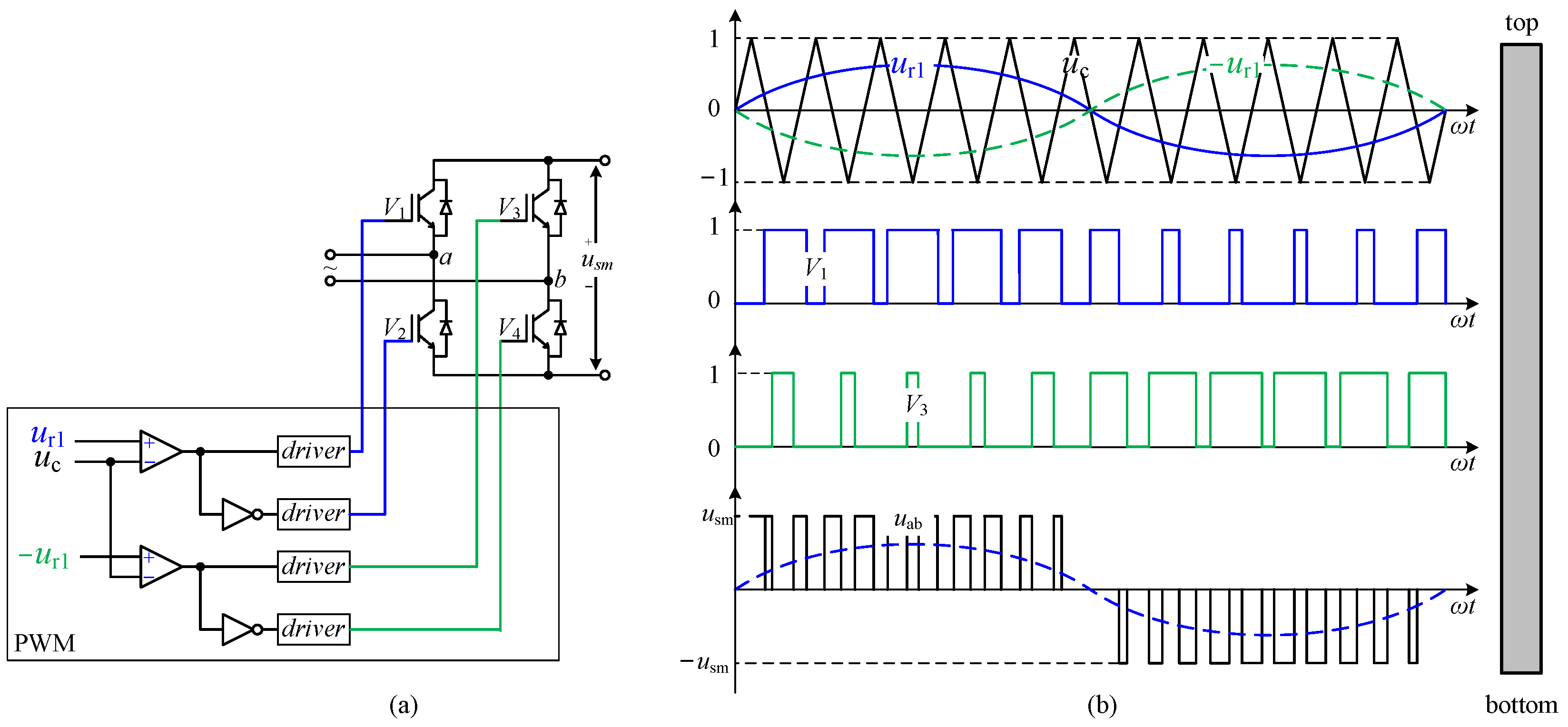
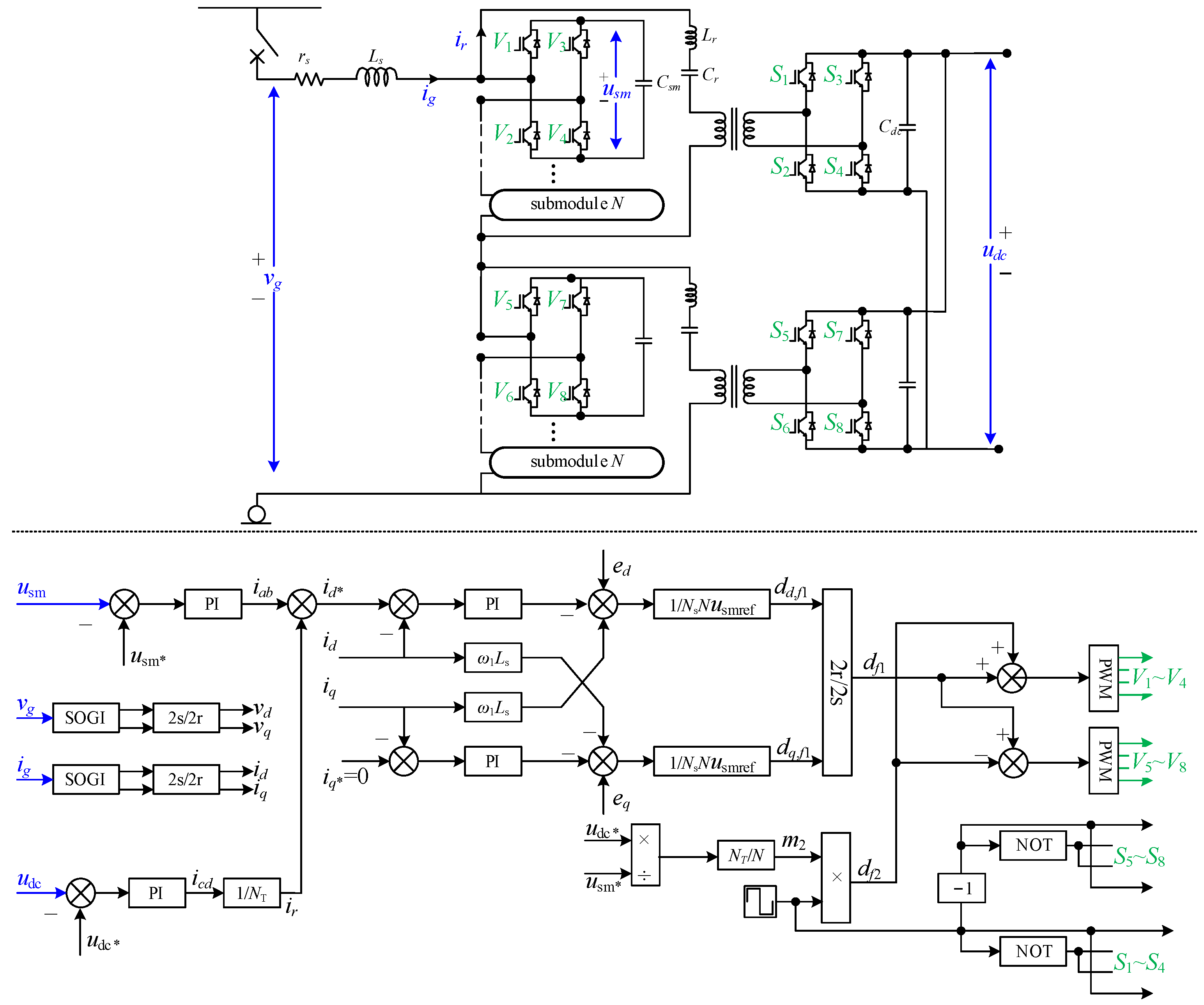
The following clarification is provided for the sake of clarity and exposition. In the proposed PETT, the H-bridge on the primary side of the MFT is designated as H1, and the H-bridge on the secondary side is designated as H2. H1 is responsible for implementing the AC/DC converter, while also forming a DC/DC converter with the MFT and H2. Furthermore, the f2 should be sufficiently high to provide a high-frequency square-wave voltage on the primary side of the MFT. It can be stated that the multiplexing of the H-bridge circuit is achieved through the utilisation of multi-frequency PWM control, which represents the operational principle of the proposed PETT. It is assumed that the hardware parameters of the cascade sub-modules in Figure 2b are identical and that the switching devices are numbered in accordance with the circuit depicted in Figure 2. It is evident that H1 comprises switching devices V1~V4 and capacitor Csm, while H2 is constituted by switching devices S1~S4 and capacitor Cdc.
The different polarities of the modulating waves allow for the classification of PWM control into unipolar and bipolar types. Each of these control methods possesses distinct advantages and disadvantages, which are contingent upon the specific application. In the case of unipolar PWM control, the AC side of the H-bridge is capable of outputting positive, negative, and neutral levels. In the case of bipolar PWM control, the H-bridge AC side outputs positive and negative levels. It is important to note that the equivalent switching frequency of unipolar PWM control is twice that of bipolar PWM modulation. Consequently, it is possible to reduce switching losses while simultaneously reducing the total harmonic distortion (THD) of the H-bridge AC-side voltage, which in turn leads to a reduction in the fluctuations in the AC-side input current. In light of the benefits associated with unipolar PWM control, this paper proposes the implementation of unipolar PWM control as the control strategy for PETTs.
Table 1 illustrates the complete set of switching combinations for V1~V4 under unipolar modulation. Here, a switching signal of “0” indicates that the device is in an off state, while a switching signal of “1” denotes that the device is in an on state. At this time, H1 exhibits the following characteristics:

Table 1.
Switching combinations of H1 under unipolar PWM control.
- (i)
- At uab > 0, the value of uab will switch between usm and 0, where usm is the voltage of the capacitor Csm on the DC side of H1.
- (ii)
- At uab < 0, the value of uab will switch between −usm and 0.
One possible PWM strategy for realising the switching combinations demonstrated in Table 1 is given in Figure 3, and several important waveforms relevant to this strategy are given.
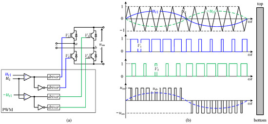
Figure 3.
PWM control strategy. (a) Control method. (b) Waveforms under PWM control (from top to bottom); carrier waveform uc; and modulating waveform ur1; control signals of switch V1; control signals of switch V3; and AC-side voltage uab.
The introduction of a three-valued logic switching function, δ, with δ = V1 − V3, allows the voltage uab and the DC-side current ism of H1 to be expressed in terms of the switching function as
where iab is the base wave current on the AC side of H1.
The non-single frequency modulation strategy adopted in this paper allows for the decomposition of the voltage uab into a sinusoidal AC component uf1 and a square-wave AC component uf2. The corresponding switching functions, designated as δf1 and δf2, respectively, enable the expression of the voltage component of uab and the DC-side current ism as
where ig is the grid current at the network side and ir is the resonant current of the LC resonant circui.
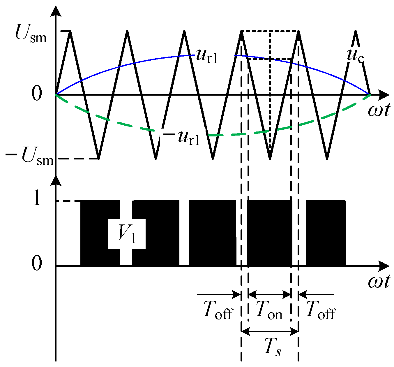
Figure 4 depicts a partially enlarged representation of Figure 3b for uab ≥ 0. It is assumed that the frequency of the triangular carrier uc is fs and that its peak value is Ucm. The rms value of usm is denoted as Usm, and it is that Ucm = Usm. If the modulation ratio of the modulating wave ur1 is m1, the modulating wave ur1 can be expressed as ur1 = m1Usmsinω1t.
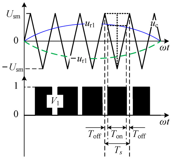
Figure 4.
Partial enlargement of Figure 3.
Figure 4 illustrates the relationship between the on-time ton of switch V1 and the period Ts of the carrier wave. Based on the similarity of triangles, Ton satisfies the following relationship with Ts:
The duty cycle function of the switch V1 when employing ur1 modulation is represented as df1(V1). By employing Equation (3), it is possible to derive the following equation: df1(V1) = 0.5 + 0.5m1sinω1t. Similarly, the duty cycle function of the switch V3 is represented as follows: df1(V3) = 0.5 − 0.5m1siω1t. If the duty cycle function corresponding to the switching function δf1 is denoted as df1, it can be expressed as df1 = m1sinω1t.
If the modulation ratio of the modulating wave ur2 is m2, the modulating wave ur2 can be expressed as
where j is an odd number.
In the context of ur2 modulation, the duty cycle functions of the switch V1 and V3 are designated as df2(V1) and df2(V3), respectively. By means of Equations (3) and (4), the following can be obtained:
The duty cycle function corresponding to the switching function δf2 is designated as df2. This can be obtained through Equation (5):
In this paper, open-loop control is used to control H2, and the on/off switching devices S1~S4 are controlled by square-wave pulses with a duty cycle of 0.5. Table 2 shows all the switching combinations of S1~S4, where a switching signal of “0” means the device is off and a switching signal of “1” means the device is on. The control process is as follows: when ucd > 0, S1 and S4 are on; when ucd < 0, S2 and S3 are on.
Table 2.
Switching combinations of H2.
The introduction of a three-valued logic switching function, σ, with σ = 2S1 − 1, allows the voltage ucd and the DC-side current idc of H2 to be expressed in terms of the switching function as
where icd is the base wave current on the AC side of H2.
If the ratio of the MFT is represented by the symbol NT, then the voltage and current on the primary and secondary sides of the MFT are satisfied:
If the duty cycle function corresponding to the switching function σ is represented by the symbol D, this is expressed as follows:
From Equations (6) and (9), it can be demonstrated that df2 = m2D. Consequently, Equations (2) and (8) can be expressed in terms of the duty cycle function as
2.2. Current Loop of the Proposed PETT
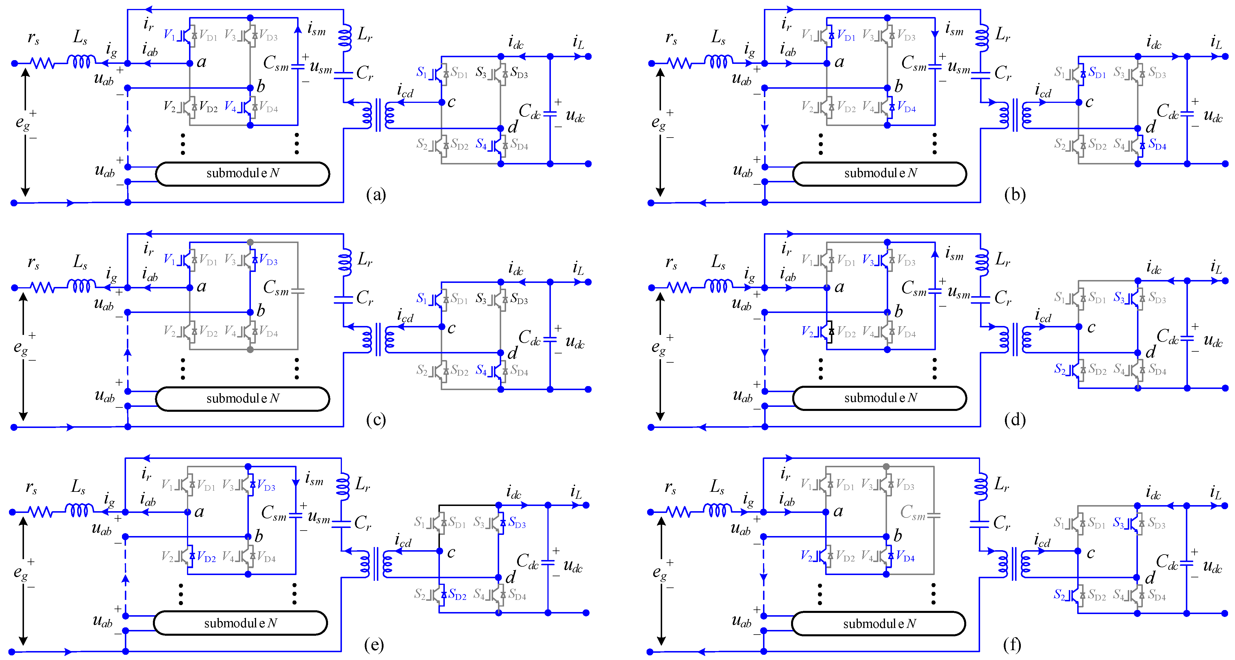
In this section, the current loop of the proposed PETT under unipolar PWM control is discussed. When eg > 0, the modes of H1 are mode 3 and mode 4. When the switching combination of H1 is in mode 3, the voltage across the inductor Ls is less than 0. Depending on the direction of the current iab, H1 possesses 2 current loops. Figure 5a,b illustrate the aforementioned two current loops. When the switching combination of H1 is in mode 4, the voltage across the inductor Ls is greater than 0. At this time, the current loop of H1 is shown in Figure 5c. The details can be analysed as follows:
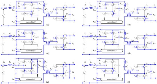
Figure 5.
Current loop of the proposed PETT. (a) iab < 0 and V1, V4, S1, S4 are on. (b) iab > 0 and V1, V4, S1, S4 are on. (c) iab < 0 and V1, V3, S1, S4 are on. (d) iab > 0 and V2, V3, S2, S3 are on. (e) iab < 0 and V2, V3, S2, S3 are on. (f) iab > 0 and V2, V4, S2, S3 are on.
In Figure 5a, iab < 0. At this point, the current iab flows into point b, through V4, the capacitor Csm, and V1, and subsequently out of point a. In this process, uab = usm, and the inductor Ls stores energy. The switching combination of H2 is in mode 5 and icd < 0. At this point, the current flows in from point d, through S4, the capacitor Cdc, and S1, and finally out from point c. In this process, ucd = udc.
In Figure 5b, iab > 0. At this point, the current iab flows in from point a, through the anti-parallel diode of V1, the capacitor Csm, and the anti-parallel diode of V4, and finally out from point b. The inductor Ls releases energy. In this process, uab = usm, and the inductor Ls releases energy. The switching combination of H2 is in mode 5 and icd > 0. At this time, the current icd current flows from point c, flows through the anti-parallel diode of S1, the capacitor Cdc, and the anti-parallel diode of S4, and finally out from point d. In this process, ucd = udc.
In Figure 5c, iab < 0. At this point, the current iab flows in from point b, flows through V1 and the anti-parallel diode of V3, and finally out from point a. In this process, uab = 0. The current loop of H2 remains the same as in Figure 5a.
When eg < 0, the modes of H1 are mode 2 and mode 1. When the switching combination of H1 is in mode 2, the voltage across the inductor Ls is greater than 0. Depending on the direction of the current iab, H1 is equipped with 2 current loops. Figure 5d,e illustrate the aforementioned two current loops. When the switching combination of H1 is in mode 1, the voltage across the inductor Ls is less than 0. At this time, the current loop of H1 is shown in Figure 5f. The specific analyses are as follows:
In Figure 5d, iab > 0. At this point, the current iab flows in from point a, flows through V2, the capacitor Csm, and V3, and finally out from point b. In this process, uab = −usm and the inductor Ls stores energy. The switching combination of H2 is in mode 6 and icd > 0. At this time, icd flows in from point c, flows through S2, the capacitor Cdc, and S3, and finally flows out from point d. In this process, ucd = −udc.
In Figure 5e, iab < 0. At this point, the current iab flows in from point b, flows through the anti-parallel diode of V3, the capacitor Csm, and the anti-parallel diode of V2, and finally flows out from point a. In this process, uab = −usm, and the inductor Ls releases energy. The switching combination of H2 is in mode 6 and icd < 0. At this point, the current icd flows from point d, through the anti-parallel diode of S3, the capacitor Cdc, and the anti-parallel diode of S2, and finally out from point c. In this process, ucd = −udc.
2.3. Mathematical Modelling of the Proposed PETT
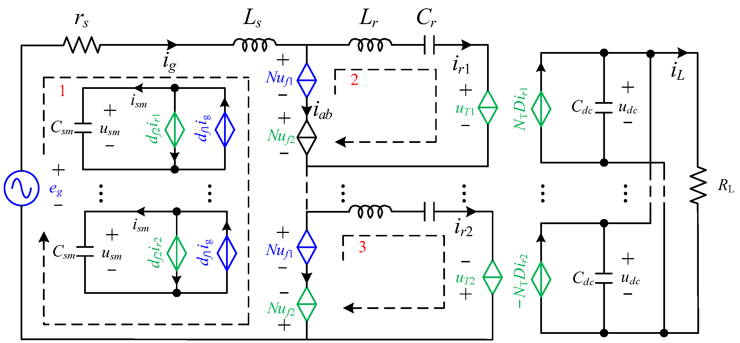
The equivalent circuit of the proposed PETT is shown in Figure 6, where half of the power unit AC-side voltages are (Nuf1 + Nuf2) and the other half of the power unit AC-side voltages are (Nuf1 − Nuf2). The loop 1 in Figure 6 is analysed and the KVL equation is written as follows:
where eg is the traction grid voltage, ig is the grid input current, Ls is the grid-side filter inductance, Ns is the number of power units, N is the number of sub-modules inside a single power unit, and uf1 is the voltage component of the sub-module AC-side voltage with frequency f1.
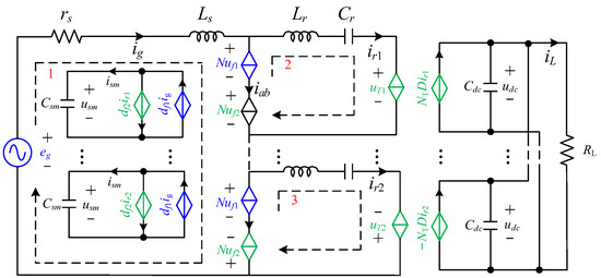
Figure 6.
An equivalent circuit of the proposed PETT.
Let us assume that the grid voltage eg is eg = Emsinω1t and the voltage component uf1 is uf1 = Em1sinω1t. From Equation (11), the first-order linear differential equation can be obtained as follows:
The solution to Equation (12) is as follows:
Considering ig(t = 0) = 0, the value of the constant c1 in Equation (13) can be obtained. Also, the phase angle φ1 is introduced and satisfied:
From the preceding analysis, it can be inferred that
Equation (15) shows that the steady-state current of ig does not contain the harmonics associated with f2, and the current ig can be expressed as ig = Imsin(ω1 − φ1).
The loop 2 in Figure 6 is analysed and the KVL equation is written as
where uT is the primary-side voltage of MFT.
Since the resonant frequency of the LC resonant circuit is the same as that of uf2, then Lr and Cr satisfy LrCr = 1/ω2. The following can be obtained:
The second-order linear differential equation can be obtained from (17):
The solution to Equation (12) is as follows:
The derivative operation on Equation (19) gives the current of the LC filter circuit as
Considering ir(t = 0) = 0, the value of the constant c2 in Equation (20) can be determined. Upon the substitution of this value into Equation (20), the result is as follows:
Equation (21) shows that the LC filter current contains harmonics related to f2. However, in the actual design, when the angular frequency ω2 is much larger than ω1, and the smaller Cr is selected as the filter capacitor, the coefficients of the first and third terms on the right side of the middle equation of Equation (20) are smaller, and the maximum or minimum value of the current ir can then be considered to be Irm = |c3|ω2Cr. Considering that the maximum transmitted power satisfies Pm = 0.5EmIm = 0.5NsNEm2Irm, the value of the constant c3 can be obtained. Upon the substitution of this value into Equation (21), the result is as follows:
Similarly, an examination of the analysis of loop 3 in Figure 6 reveals that
The presence of time-varying AC quantities in the mathematical model obtained is not favourable for control system design. It is also necessary to transform it into a mathematical model in the dq coordinate system by means of coordinate transformation. For single-phase systems, a virtual orthogonal component must be constructed when performing coordinate transformation. In this paper, we will construct the virtual β-axis orthogonal to the α-axis by delaying a quarter cycle, then construct the αβ coordinate system, and finally complete the construction of the dq coordinate system.
The mathematical model of the proposed PETT in the coordinate system of the dq coordinate system is as follows:
where Req is the equivalent load of a single power unit, Req = RL/Ns.
3. Control Strategy of the Proposed PETT
In the field of PWM converter control, the double closed-loop strategy is a well-established approach that offers the benefits of a rapid dynamic response and high interference immunity [27,28,29,30,31]. Typically, this strategy comprises voltage outer-loop control and current inner-loop control. For the PETT circuit under consideration, the double closed-loop control represents a straightforward and effective control strategy.
3.1. Analyse of the Current Inner-Loop Control System
The present loop control circuit is designed in accordance with the specifications set forth in Equation (24). Given the symmetry between the iq current loop and the id current loop, the design method for the latter will be outlined in this section. When the PI controller is employed as the current controller and feedforward control quantities are introduced, the control equation can be designed as follows:
where kp1 and ki1 are the proportional and integral regulation gains of the current controller, respectively; id* is the command value of the current id; iq* is the command value of the current iq; and the third term on the right side of the equation is the feed-forward control quantity.
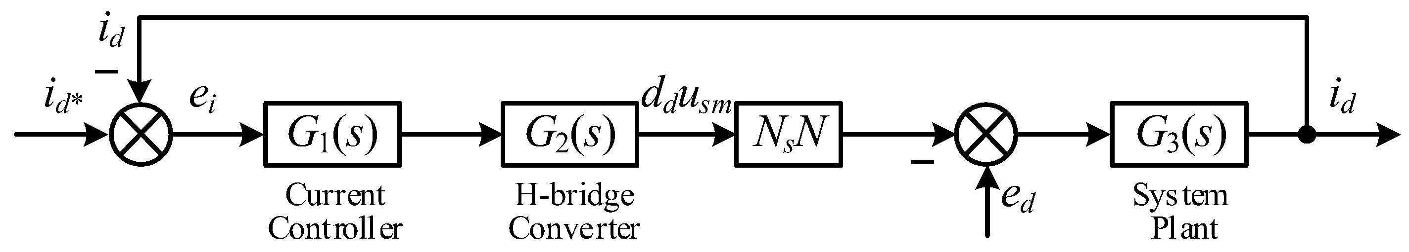
The current loop, illustrated in Figure 7, is constructed in accordance with Equation (25). In Figure 7, G1(s) is the transfer function of the id current controller. G2(s) is the transfer function of the H-bridge converter under PWM control. G3(s) is the open-loop transfer function of the system unit. The specific expression for the aforementioned transfer functions is as follows:
where Ti is the sampling period of the current loop and is the same as the switching period Ts, meaning that Ti = Ts.

Figure 7.
Structure of id current loop control system after decoupling.
In the absence of the consideration of ed, the open-loop transfer function of the id current loop can be expressed as follows:
Equation (27) shows that the id current loop comprises two poles, namely, s1= −1/Ti and s2 = −Ls/rs. In the majority of cases, the main pole is identified as s2 due to the considerable value of fi. In order to achieve a faster response, it is possible to utilise the controller’s zeros in order to offset s2. This can be achieved by setting kp1/ki1 = Ls/rs. At this juncture, the switching function F1(s) is as follows:
Then, the closed loop transfer function of the id current loop is as follows:
3.2. Analysis of the Voltage Outer-Loop Control System
The present loop control voltage is designed in accordance with the specifications set forth in (24). When the PI controller is employed as the voltage controller, the control equation can be designed as
where kp2 and ki2 are the proportional adjustment gain and integral adjustment gain of the voltage usm controller; kp3 and ki3 are the proportional adjustment gain and integral adjustment gain of the voltage udc controller; usm* is the command value of the voltage usm; and udc* is the command value of the voltage udc.
Considering the preceding analysis, it can be assumed that ig = Imsin(ω1t − φ1) and ir = Irmsinω2t. With regard to the DC-side fundamental wave and double frequency fluctuation, the DC-side current component of H1 can be expressed as follows:
The voltage loop, illustrated in Figure 8, is constructed in accordance with Equation (30). In Figure 8, G4(s) and G6(s) are the transfer functions of the usm voltage controller and the udc voltage controller, respectively. G5(s), G7(s), and G8(s) are the open-loop transfer functions of the system devices. The specific expression for the aforementioned transfer functions is as follows:
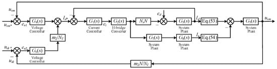
Figure 8.
Structure of voltage loop control system.
As illustrated in Figure 8, both Equations (31) and (32) are time-varying links. This introduces challenges in the design of the voltage loop, which can be addressed by considering the maximum proportional gain of the link as a potential replacement. In the absence of the consideration of the ed, the equivalent structure diagram, as illustrated in Figure 9, is obtained through the simplification of the control structure diagram, as shown in Figure 8. This is achieved through the combination of comparison points, the shifting of the lead point backwards, and the application of series equivalence and parallel equivalence.
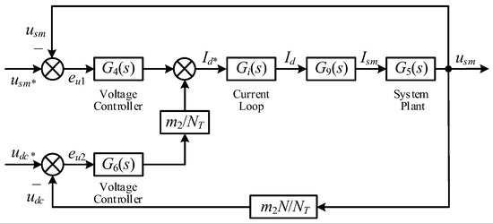
Figure 9.
Equivalent structure of voltage loop control system.
In Figure 9, the specific expression of G9(s) is as follows:
When udc* = 0, the open-loop transfer function between the input signal usm* and the output signal usm can be obtained as follows
When usm* = 0, the open-loop transfer function between the input signal udc* and the output signal usm can be obtained as follows
3.3. Integrated Control Strategy
In summary, the overall control block diagram of the proposed PETT is presented in Figure 10. The voltage control loop employs PI controllers, while the control voltages usm and udc adhere to the prescribed values of usm* and udc*, respectively. The outputs of the aforementioned controllers are employed as inputs to the current loop following the implementation of requisite arithmetic operations. Subsequently, the modulating signal waveform, designated as df1, is generated following the completion of the current loop and coordinate transformation. The values of m2 are then obtained through the operation of usm* and udc*. This, in turn, generates the aforementioned modulating signal waveform, designated as df2. Subsequently, the aforementioned two modulating signals (df1 and df2) are superimposed, whereupon PWM modulation is performed. The resulting output is the control signal for H1. In conclusion, a fixed-frequency square-wave pulse is employed as the control signal for H2.
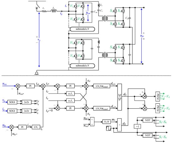
Figure 10.
The control strategy adopted for the proposed PETT.
The extensive use of power electronic equipment will inevitably result in an increase in the total harmonic distortion (THD) of the incoming current. Improvements in THD can be achieved through the optimisation of the topology, the enhancement of the hardware performance, and the optimisation of the control algorithm, with the objective of ensuring the power quality. When the proposed PETT adopts the control strategy shown in Figure 10, the PWM control can be combined with the selective harmonic elimination (SHE) technique to eliminate the lower harmonics and reduce the THD value under the traditional PWM control while also ensuring the fundamental amplitude. This method necessitates only minimal alterations to the control circuit and is straightforward to implement. Furthermore, the introduction of a harmonic compensator can serve to mitigate the effects of harmonic currents. By rotating the positive-sequence component of the kth harmonic by kω1 while the negative-sequence component rotates by −kω1, a mathematical model of the controlled object in the kth harmonic rotating coordinate system is obtained. This model is then used to design the parameters of the harmonic compensator. This scheme necessitates a significant alteration to the control circuit. As the improvement of the THD is not the primary objective of this study, a detailed examination of this topic is not provided here.
3.4. Loss Analysis of the Proposed PETT
A reasonable loss analysis constitutes an essential component of the converter design process. Calculating the power loss of the converter and subsequently predicting the efficiency of the converter facilitates the subsequent optimisation of the converter’s efficiency. Concurrently, forecasting the temperature distribution of the switching devices and magnetic components supports subsequent work on the thermal design of the entire machine. This section presents a discussion of the power loss, including the conduction loss and switching loss, caused by the proposed PETT switching under the control strategy illustrated in Figure 10. The discussion employs an N-channel type IGBT module as a case study.
- (i)
- Conduction loss
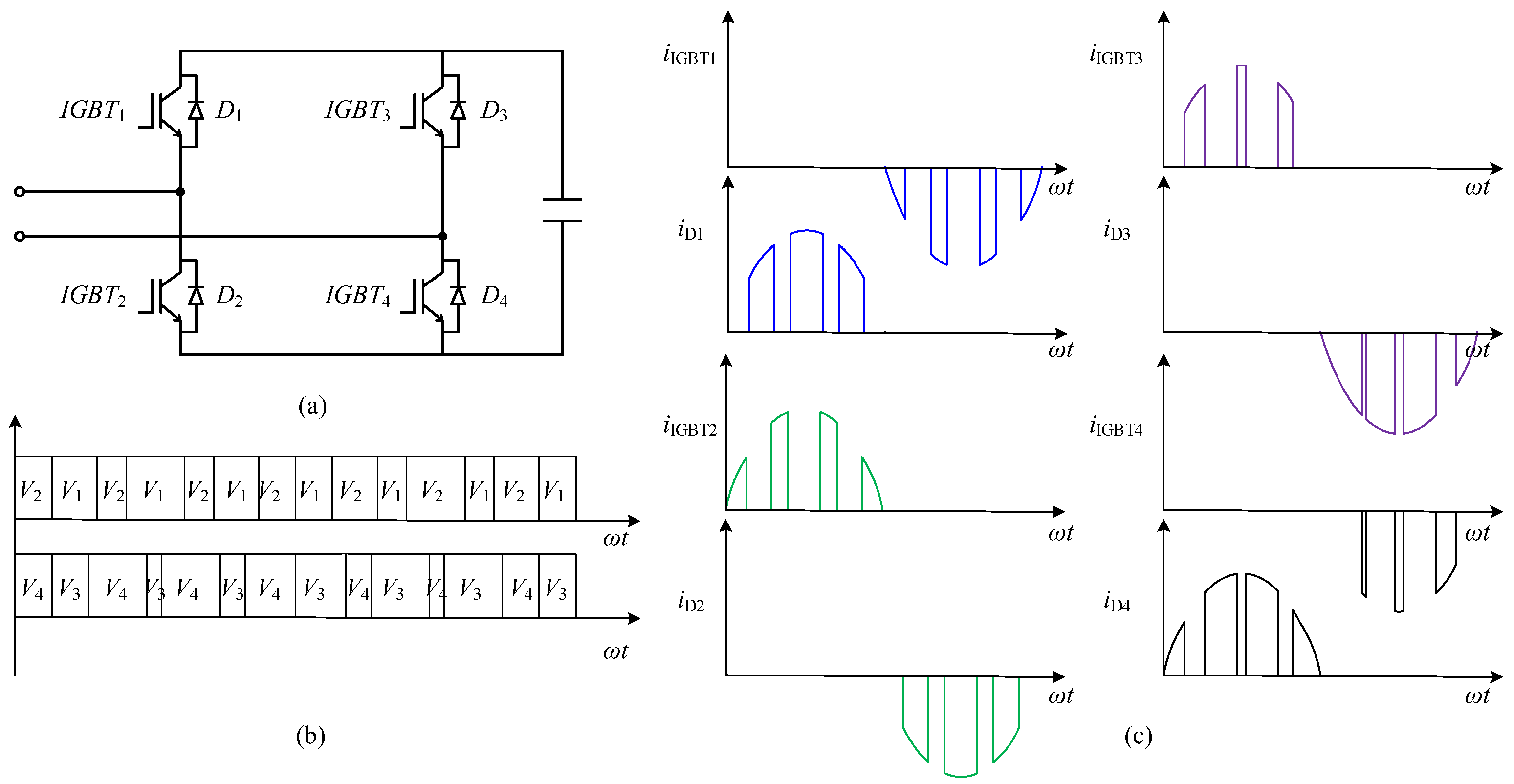
Upon the activation of the IGBT module, two distinct operational states are observed: forward conduction and reverse conduction (anti-parallel diode conduction). Figure 11 illustrates the conduction sequence of the switching devices and the current waveforms flowing through the IGBTs and diodes in H1 under unipolar PWM control.
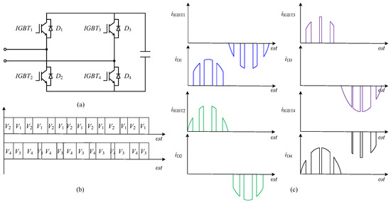
Figure 11.
Current waveforms of switching devices in H1 under unipolar PWM control. (a) H-bridge circuit. (b) Switch conduction sequence. (c) Current waveform of each switching device in one operating cycle.
As illustrated in Figure 11, at each current cycle, both the IGBT and the diode are operational for only half of the cycle. Let us consider first that the conduction loss of a single IGBT when the modulating waveform is sinusoidal (frequency f1) is as follows:
where Tf1 is the operating period of the IGBT, df1(t) is the duty cycle function, ice(t) is the on-state current, and vce(t) is the on-state voltage drop. The latter is solved by the following (38):
where uce0 and rce are obtained from the IGBT output characteristic curve provided by the IGBT manufacturer.
It has been previously established that ice(t) = Imsin(ω1t − φ1) and df1(V1) = 0.5 + 0.5m1sinω1t. Upon substituting ice(t) and df1(t) into (37) and (38), the conduction loss of a single IGBT in one operating cycle is obtained as follows:
Similarly, the conduction loss of a single diode in one operating cycle is obtained as follows:
where ut0 and rt are obtained by means of diode output characteristic curves provided by the manufacturer.
Next, let us consider the calculation of the conduction loss of a single IGBT and diode when the modulating waveform is a square wave (frequency f2). It was previously shown that id(t) = Irmsin(ω2t). The duty cycle function is shown in Equation (5). This information can be used to determine the following:
- (ii)
- Switching loss
Switching loss is the loss generated during the turn-on and turn-off process of power electronic devices, including turn-on loss and turn-off loss. Switching losses can be obtained by both estimation and experimental measurement.
Approximating the switching process to be linear, the switching losses are estimated by using the voltage and current values at turn-on or turn-off, as are the rise and fall times. Alternatively, using the manuals provided by the device manufacturers, the switching losses under standard conditions are read and the switching losses are estimated based on the actual temperature, voltage, and current. Let us consider the parasitic parameters in the switching device, including the parasitic capacitance and parasitic inductance. The switching process of the device is not linear, and so the switching loss obtained by the prediction method is incorrect in relation to the actual loss. This also requires that more accurate switching loss predictions should be obtained through experimental calculations in situations where efficiency optimisation is required.
4. Parametric Design of the Proposed PETT
Grid-side inductance Ls affects the value of the DC-side voltage usm of H1 and the waveform quality of the input current ig. In addition, it places a limit on the maximum amount of power that can be transmitted. In the design of inductor Ls, it is essential to consider the metric of transient current tracking.
- (i)
- When the current ig crosses zero, the rate of change of the current reaches its maximum value. In order to ensure the rapidity of the current response, the value of the inductor Ls should be as small as possible.
- (ii)
- Near the peak value of current ig, harmonic pulsation is at its most serious. In order to suppress the harmonic current, the value of inductor Ls should be as large as possible.
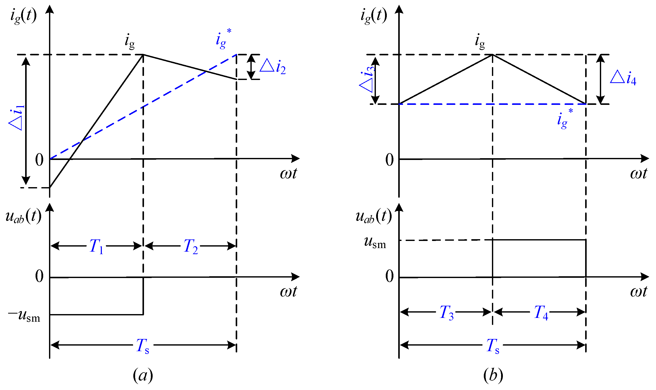
In order to initiate the analysis, two switching cycles were selected: one near the current value of ig = 0 and one near the peak value of ig. The resulting tracking waveform of ig is presented in Figure 12. Figure 12a corresponds to one switching cycle in which the value of eg changes from a negative to a positive value, while Figure 12b corresponds to one switching cycle in which the value of eg is positive and the value of ig reaches its peak.
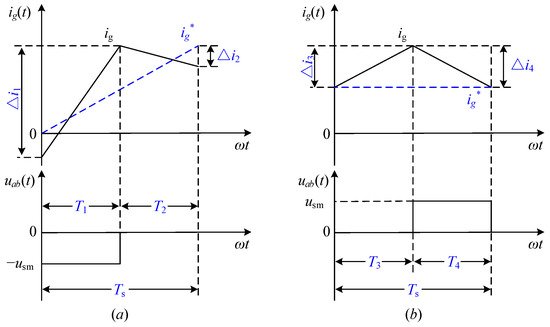
Figure 12.
Current tracking waveforms during one switching cycle at special moments. (a) ig = 0. (b) ig = igm.
In steady-state conditions, the value of the grid voltage eg can be considered to be constant at 0 for one switching cycle, as illustrated in Figure 12a. If the effect of rs is disregarded, the following system of equations is derived:
In order to facilitate the rapid advancement of the command current by the ig, it is essential to satisfy the following equation:
Since the value of the switching period Ts is sufficiently small, sin(ω1Ts)/Ts ≈ ω1. The range of values of Ls can be determined by Equations (43) and (44) as follows:
In steady-state conditions, the value of the grid voltage eg can be considered to be constant at Em for one switching cycle, as illustrated in Figure 12b. If the effect of rs is disregarded, the following system of equations is derived:
Considering that |Δi3| = |Δi4| and T3 + T4 = Ts, the pulsation of current ig can be obtained from (46) as follows:
If the maximum value of current pulsation is Δimax, then the range of values of Ls can be determined as follows:
In conclusion, in order to satisfy the metric of transient current tracking, the value of Ls must satisfy the following inequality:
The DC-side capacitor (Csm) of H1 serves two distinct functions: firstly, it stabilises the DC-side voltage, and secondly, it suppresses the DC-side harmonic voltage. In the case of H1, the instantaneous value component of the input power on the AC side can be expressed as follows:
Equation (50) shows that the instantaneous power on the AC side of H1 consists of two parts, the DC and AC power. Similarly, the instantaneous power on the DC side of H1 should also consist of two parts, namely, the average power consumed by the load and the ripple power of the ripple current flowing through the capacitor. The instantaneous power on the DC side can be expressed as follows:
where Δusm is the output DC ripple voltage value of H1.
It is assumed that the power loss of the IGBT is not considered. In accordance with the law of energy conservation, the instantaneous input power of the H-bridge converter is approximately equal to the instantaneous output power on the DC side. This is expressed as follows:
The integration of both sides of Equation (52) results in the following:
If the maximum allowable pulsation value of usm is denoted as Δumax1, then Δumax1 ≥ 2Δusm needs to be satisfied. According to Equation (53) the range of values of Csm can be determined as follows:
Similarly, the range of values of Cdc can be determined as follows:
where Δumax2 is the maximum allowable pulsation value of udc.
5. Simulation Analysis
In order to ascertain the efficacy of the proposed PETT circuit, a 1.2 MW PETT was designed and presented in this paper. The specifications of the traction grid included 15 kV/16.7 Hz. The sub-module had a DC-side voltage of 3.6 kV and a DC output voltage of 1.2 kV. Based on the design methodology outlined in Section 2, Section 3 and Section 4, the design flow of the main circuit parameters of the proposed PETT is shown in Figure 13. The principal circuit parameters of the PETT can be derived from Figure 13. The fundamental characteristics of the proposed PETT circuit are presented in Table 3.
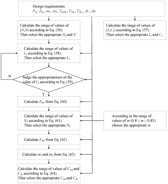
Figure 13.
The design flow of the proposed PETT main circuit parameters.
Table 3.
Parameters of PETT.
In Figure 13, Equations (56)–(64) are specifically expressed as follows:
where Em is the peak value of the phase voltage, in this case the value of 12,247 V, and Usm is the design value of the sub-module capacitance voltage, in this case the value of 3600 V.
where ω2 is the resonant frequency of the filter, which in this case takes the value of 2000 Hz.
where Pm is the maximum transmitted power, which is taken here as 1.2 MW; TPWM is the switching period of H1, which is taken here as 10,000 Hz; ω1 is the frequency of the grid voltage, which is taken here as 16.7 Hz; and Δi is the maximum permissible value of the current ripple, which is taken here as 5%.
where Udc is the design value of the output DC voltage of the PETT, which in this case is taken as 1200 V.
where Δu is the maximum permissible value of the capacitor voltage ripple, which in this case is taken as 3%.
The PET prototype, designed in accordance with Figure 1 and detailed in Table 4, is compared with the designed PETT in this paper. It is observed that the proposed PETT employs a reduced number of sub-modules, switching devices, capacitors, and MFTs. It is shown that the proposed PETT has the advantage of requiring a reduced number of power devices and passive components under the condition of the same grid voltage, the same IGBT voltage level, and the same output voltage. Furthermore, this advantage is more pronounced when non-high-voltage IGBTs are employed.
Table 4.
The cascade PETT design of different structures.
In order to ascertain the veracity of the designed PETT circuit, a simulation model was constructed and analysed using PLECS 4.2. The simulation parameters are presented in Table 3. The simulation process is as follows: at 0 ≤ t < 3 s, the PETT operates at the rated load. At 3 s ≤ t < 6 s, the PETT operates at 80% of the rated load. At 6 s ≤ t < 9 s, the PETT operates at 60% of the rated load.
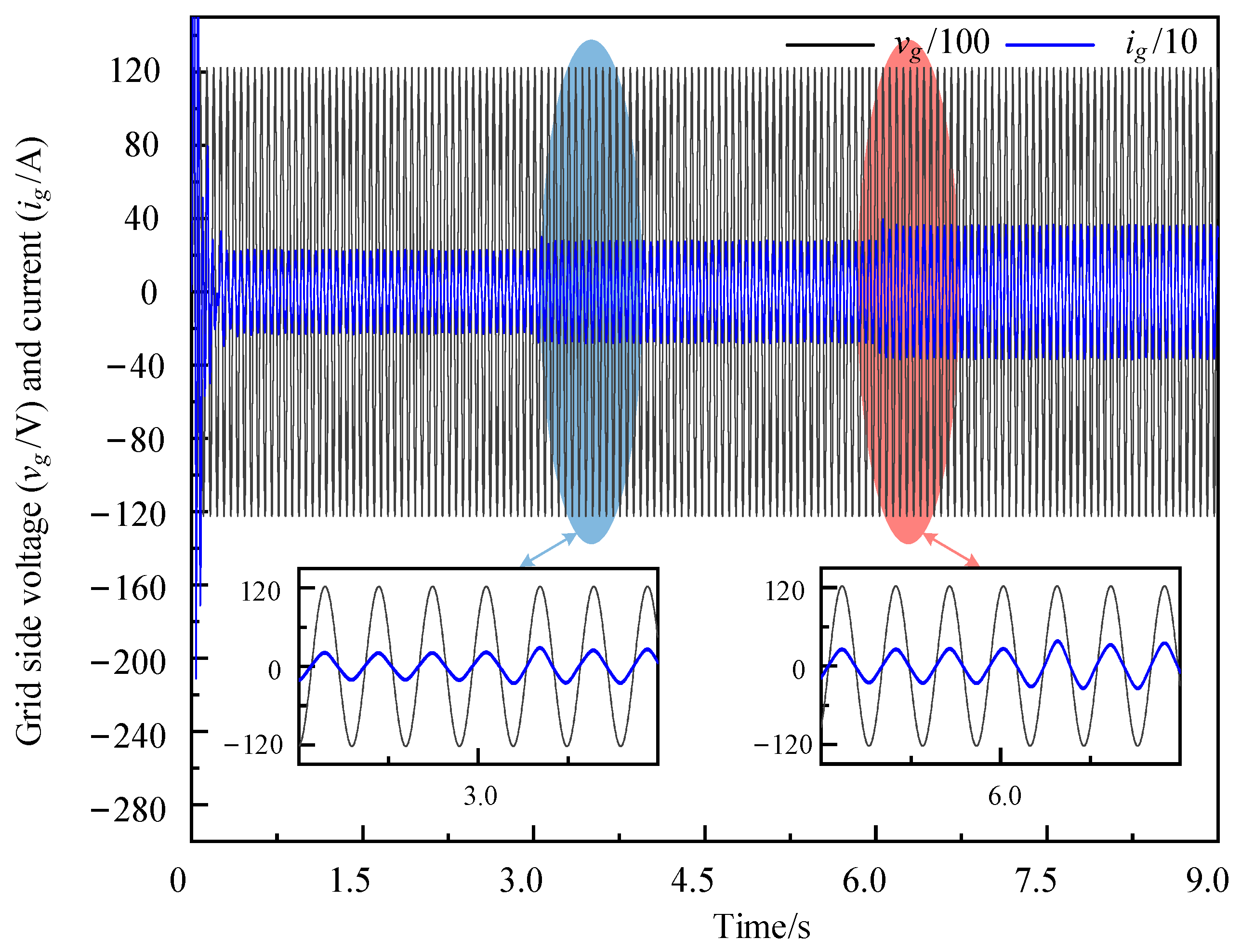
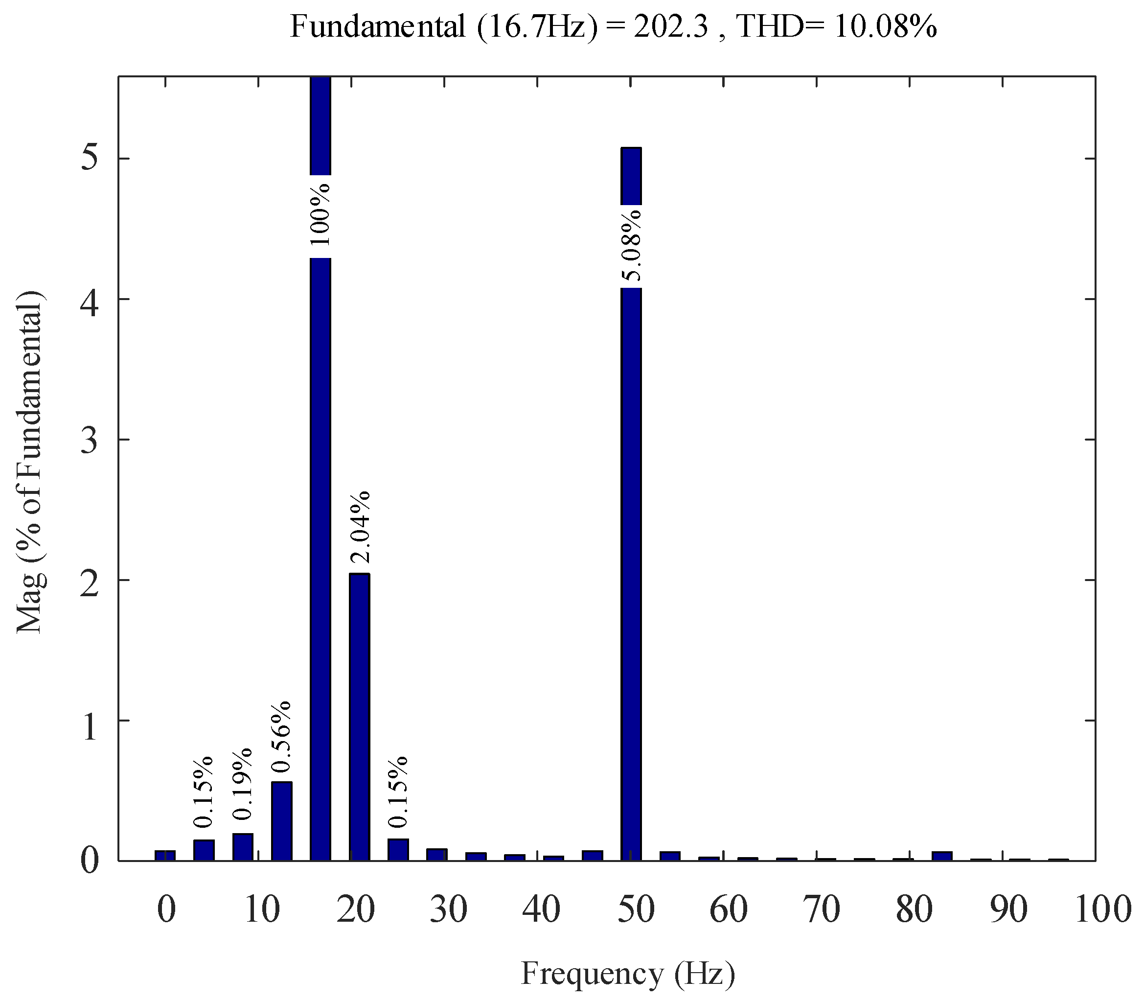
Figure 14, Figure 15, Figure 16, Figure 17 and Figure 18 show the simulation results of some physical quantities at the primary side of the IF transformer. Specifically, Figure 14 gives the waveforms of current ig and voltage eg at the grid side of the PETT. When the PETT is running stably, the sinusoidal nature of the current is good, the power factor is kept at 1, and the voltage waveform can be tracked. The calculated value of the peak current is 195.96 A at a rated load and the simulation yields a peak value of 202.3 A with an error of 3%. At t = 3 s and t = 6 s, the sudden change in load causes a short oscillation in the current, which can quickly reach a steady state, and the peak current increases after stabilisation. The results of FFT analysis of the grid side current at rated load are given in Figure 15, which shows a THD of 10.08%.

Figure 14.
Network-side voltages and currents, and their local magnification.

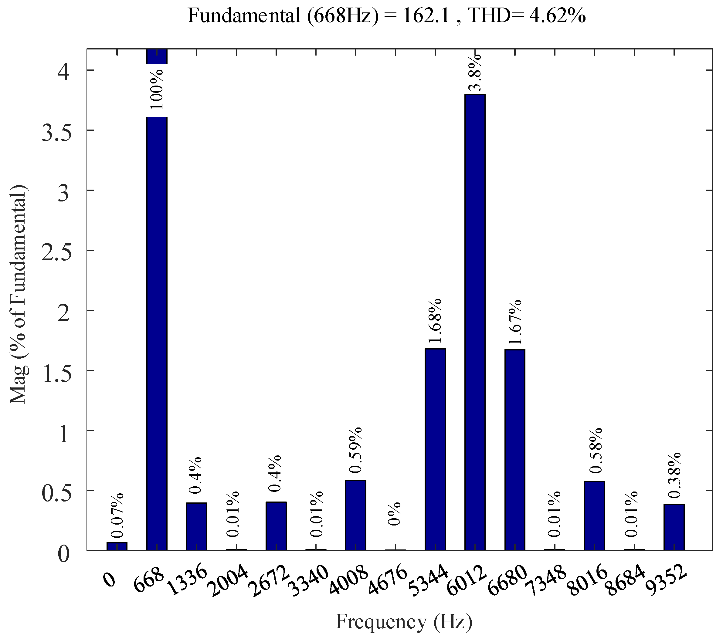
Figure 15.
FFT analysis of network-side currents.
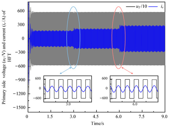
Figure 16.
Primary-side voltages and currents of MFT.

Figure 17.
FFT analysis of primary-side currents of MFT.
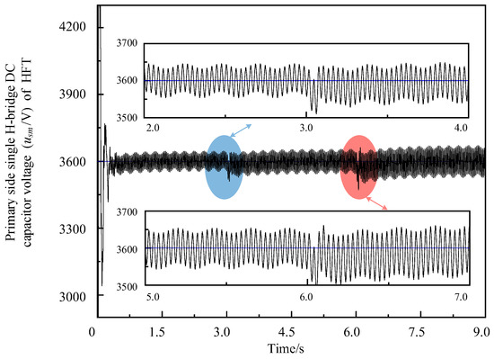
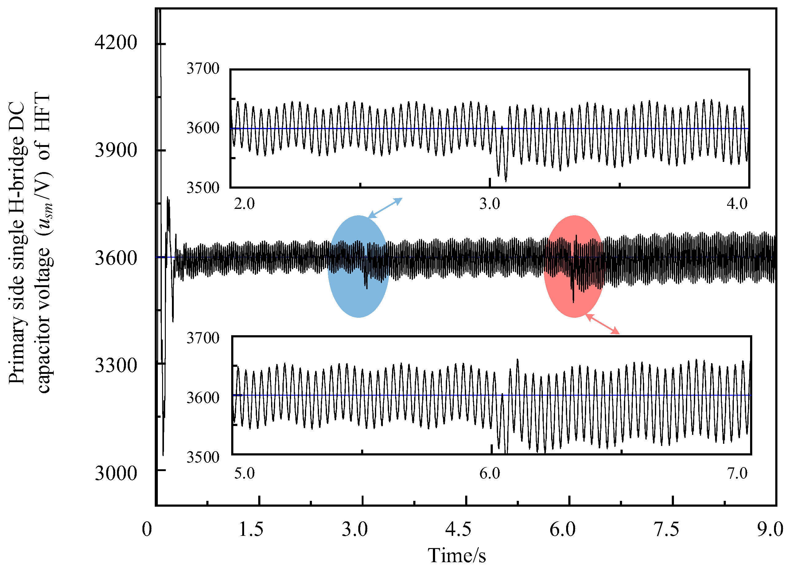
Figure 18.
Voltage of capacitor Csm of H1.
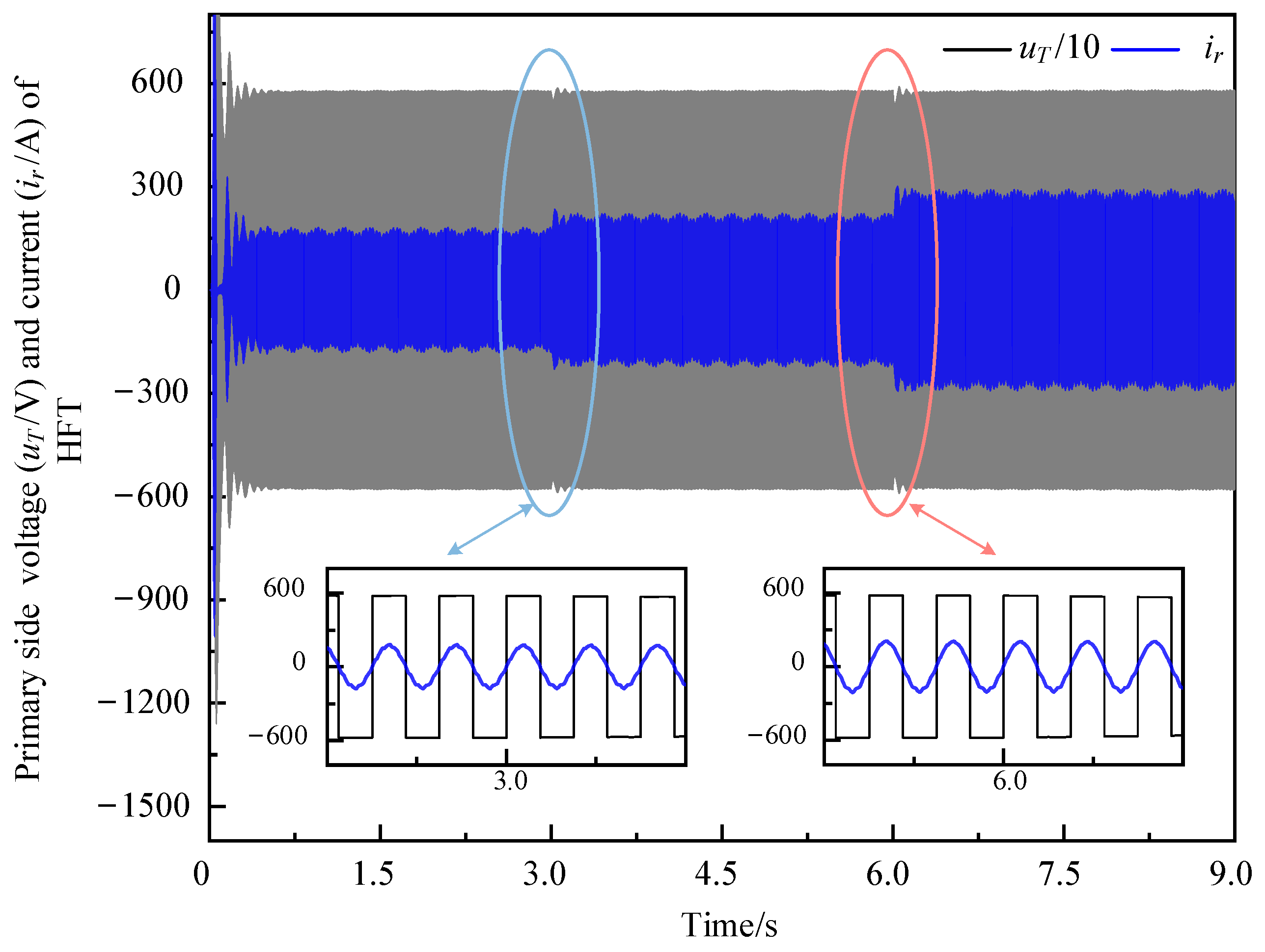
Figure 16 illustrates the waveforms of the current ir and voltage uT at the primary side of the MFT. uT is a square wave with a frequency of 668 Hz when the PETT is running stably, and the current ir is of the same frequency and the same phase as uT. Under the rated load, the peak value of voltage uT is 5760 V, and the peak value of current ir is 166 A. At t = 3 s and t = 6 s, the sudden change in the load causes a brief oscillation in the current, which can quickly reach a steady state. The peak value of the current increases after stabilisation, and the peak value of the voltage remains unchanged after stabilisation. Figure 17 gives the results of FFT analysis of ir at rated loads, showing a THD of 4.62%.
Figure 18 gives the waveforms of the voltage of capacitor Csm in H1. The value of the voltage usm is 3600 V during the stable operation of the PETT, which agrees with the design value. The ripple of the stabilised voltage is 1.1%, 1.4%, and 1.8% at different operating points. These values meet the design requirements. At the moment of a sudden load change, the usm stabilises again faster.
Figure 19 shows the waveforms of the voltage of capacitor Cdc in H2. The value of the voltage udc is 1200 V during the stable operation of the PETT, which matches the design value. The ripple of the stabilised voltage is 0.50%, 0.58%, and 0.71% at different operating periods, which meets the design requirements. At the moment of a sudden load change, udc stabilises again faster.
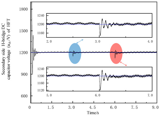
Figure 19.
The voltage of capacitor Cdc of H2.
6. Conclusions
Cascaded PTETTs are considered effective in terms of reducing the number of conventional low-frequency transformers in locomotives, with the advantages of light weight, small size, and high efficiency. However, the issue of the large number of switching devices and passive components in this type of converter cannot be ignored. In this paper, a novel PETT structure is introduced, and its feasibility is verified by theoretical analysis and simulation. The results show that the proposed PETT can achieve the multiplexing of the H-bridge through effective control, and the voltages at different frequencies are decoupled. The grid-side current can track the grid voltage better and achieve unit power factor operation. The sub-module capacitor voltage and output DC voltage can be better controlled to be in accordance with the design’s value and reach the steady state again faster when the load changes abruptly. Finally, the proposed PETT has positive significance, with reduced size and weight in relation to other PETTs and increased the power density.
Voltage equalisation strategies between multiple sub-modules of the proposed PETT will also be explored in the future. In addition, the development of accurate loss models will help to design more efficient PETTs, and these studies will further deepen the research on the proposed PETT and enable the successful use of the prototype on a locomotive.
Author Contributions
Conceptualization, B.H., Y.L. and Y.T.; methodology, B.H. and Y.L.; software, B.H.; validation, B.H.; formal analysis, B.H.; investigation, B.H.; resources, B.H.; data curation, B.H.; writing, B.H.; visualisation, Y.L.; supervision, Y.L. and Y.T.; project administration, Y.L. and Y.T. All authors have read and agreed to the published version of the manuscript.
Funding
This research received no external funding.
Data Availability Statement
The data used to support the findings of this study are included in the article.
Conflicts of Interest
The authors declare no conflicts of interest.
References
- Zhang, J.; Liu, J.; Zhong, S.; Yang, J.; Zhao, N.; Zheng, T.Q. A Power Electronic Traction Transformer Configuration with Low-Voltage IGBTs for Onboard Traction Application. IEEE Trans. Power Electron. 2019, 34, 8453–8467. [Google Scholar] [CrossRef]
- Dujic, D.; Zhao, C.; Mester, A.; Steinke, J.K.; Weiss, M.; Lewdeni-Schmid, S.; Chaudhuri, T.; Stefanutti, P. Power Electronic Traction Transformer-Low Voltage Prototype. IEEE Trans. Power Electron. 2013, 28, 5522–5534. [Google Scholar] [CrossRef]
- Zhao, C.; Dujic, D.; Mester, A.; Steinke, J.K.; Weiss, M.; Lewdeni-Schmid, S.; Chaudhuri, T.; Stefanutti, P. Power Electronic Traction Transformer—Medium Voltage Prototype. IEEE Trans. Ind. Electron. 2014, 61, 3257–3268. [Google Scholar] [CrossRef]
- Zhao, C.; Weiss, M.; Mester, A.; Lewdeni-Schmid, S.; Dujic, D.; Steinke, J.K.; Chaudhuri, T. Power electronic transformer (PET) converter: Design of a 1.2 MW demonstrator for traction applications. In Proceedings of the International Symposium on Power Electronics Power Electronics, Electrical Drives, Automation and Motion, Sorrento, Italy, 20–22 June 2012; pp. 855–860. [Google Scholar]
- Dujic, D.; Steinke, G.K.; Bellini, M.; Rahimo, M.; Storasta, L.; Steinke, J.K. Characterization of 6.5 kV IGBTs for high-power medium-frequency soft-switched applications. IEEE Trans. Power Electron. 2014, 29, 906–919. [Google Scholar] [CrossRef]
- Besselmann, T.; Mester, A.; Dujic, D. Power electronic traction transformer: Efficiency improvements under light-load conditions. IEEE Trans. Power Electron. 2014, 29, 3971–3981. [Google Scholar] [CrossRef]
- Taufiq, J. Power Electronics Technologies for Railway Vehicles. In Proceedings of the 2007 Power Conversion Conference—Nagoya, Nagoya, Japan, 2–5 April 2007; pp. 1388–1393. [Google Scholar]
- Youssef, M.; Abu Qahouq, J.A.; Orabi, M. Analysis and design of LCC resonant inverter for the tranportation systems applications. In Proceedings of the 2010 Twenty-Fifth Annual IEEE Applied Power Electronics Conference and Exposition (APEC), Palm Springs, CA, USA, 21–25 February 2010; pp. 1778–1784. [Google Scholar]
- Glinka, M. Prototype of multiphase modular-multilevel-converter with 2 MW power rating and 17-level-output-voltage. In Proceedings of the 2004 IEEE 35th Annual Power Electronics Specialists Conference (IEEE Cat. No.04CH37551), Aachen, Germany, 20–25 June 2004. [Google Scholar] [CrossRef]
- Kolar, J.W.; Ortiz, G.I. Solid-state-transformers: Key components of future traction and smart grid systems. In Proceedings of the International Power Electronics Conference—ECCE Asia (IPEC 2014), Hiroshima, Japan, 18–21 May 2014; pp. 18–21. [Google Scholar]
- Zhao, T.; Wang, G.; Bhattacharya, S.; Huang, A.Q. Voltage and Power Balance Control for a Cascaded H-Bridge Converter-Based Solid-State Transformer. IEEE Trans. Power Electron. 2013, 28, 1523–1532. [Google Scholar] [CrossRef]
- Costa, L.; Carne, G.; Buticch, G.; Liserre, M. The smart transformer: A solid-state transformer tailored to provide ancillary services to the distribution grid. IEEE Power Electron. Mag. 2017, 4, 56–67. [Google Scholar] [CrossRef]
- Huber, J.E.; Böhler, J.; Rothmund, D.; Kolar, J.W. Analysis and cell-level experimental verification of a 25 kW All-SiC isolated front end 6.6 kV/400 V AC-DC solid-state transformer. CPSS Trans. Power Electron. Appl. 2017, 2, 140–148. [Google Scholar] [CrossRef]
- Huber, J.E.; Kolar, J.W. Optimum Number of Cascaded Cells for High-Power Medium-Voltage AC–DC Converters. IEEE J. Emerg. Sel. Top. Power Electron. 2017, 5, 213–232. [Google Scholar] [CrossRef]
- Ortiz, G.; Leibl, M.; Kolar, J.W.; Apeldoorn, O. Medium frequency transformers for solid-state-transformer applications—Design and experimental verification. In Proceedings of the 2013 IEEE 10th International Conference on Power Electronics and Drive Systems, Kitakyushu, Japan, 22–25 April 2013; pp. 1285–1290. [Google Scholar]
- Huang, A.Q.; Zhu, Q.; Wang, L.; Zhang, L. 15 kV SiC MOSFET: An enabling technology for medium voltage solid state transformers. Trans. Power Elect Ronice Appl. 2017, 2, 118–130. [Google Scholar] [CrossRef]
- Zhang, X.; Xu, Y.; Xiao, X. A High Power Density Resonance Cascaded H-Bridge Solid-State Transformer for Medium and High Voltage Distribution Network. Trans. China Electrotech. Soc. 2018, 33, 310–321. [Google Scholar] [CrossRef]
- Han, X.; Liao, Y.; Yang, D. Model Predictive Control Strategy for DAB-LLC Hybrid Bidirectional Converter Based on Power Distribution Balance. IEEE Trans. Circuits Syst. II: Express Briefs 2024, 71, 3236–3240. [Google Scholar] [CrossRef]
- Morsali, P.; Dey, S.; Mallik, A.; Akturk, A. Switching Modulation Optimization for Efficiency Maximization in a Single-Stage Series Resonant DAB-Based DC–AC Converter. IEEE J. Emerg. Sel. Top. Power Electron. 2023, 11, 5454–5469. [Google Scholar] [CrossRef]
- Tan, X.; Ruan, X. Equivalence Relations of Resonant Tanks: A New Perspective for Selection and Design of Resonant Converters. IEEE Trans. Ind. Electron. 2016, 63, 2111–2123. [Google Scholar] [CrossRef]
- Nayak, S.; Das, A. A DAB based Folder-Unfolder circuit in Cascaded H-Bridge Converter for MV Grid Application. In Proceedings of the 2022 IEEE International Conference on Power Electronics, Drives and Energy Systems (PEDES), Jaipur, India, 14–17 December 2022; pp. 1–6. [Google Scholar]
- Gao, F.; Li, Z.; Wang, P.; Xu, F.; Chu, Z.; Sun, Z.; Li, Y. Prototype of smart energy router for distribution DC grid. In Proceedings of the 2015 17th European Conference on Power Electronics and Applications (EPE’15 ECCE-Europe), Geneva, Switzerland, 8–10 September 2015; pp. 1–9. [Google Scholar]
- Zhang, X.; Xu, Y.; Long, Y.; Xu, S.; Siddique, A. Hybrid-Frequency Cascaded Full-Bridge Solid-State Transformer. IEEE Access 2019, 7, 22118–22132. [Google Scholar] [CrossRef]
- Zhao, C.; Zhang, C.; Jiang, Q. An H-Bridge Time-Sharing Multiplexing-Based Power Electronic Transformer. IEEE J. Emerg. Sel. Top. Power Electron. 2023, 11, 4831–4840. [Google Scholar] [CrossRef]
- Li, Y.; Li, Y.W.; Tian, H.; Zargari, N.R.; Cheng, Z. A Modular Design Approach to Provide Exhaustive Carrier-Based PWM Patterns for Multilevel ANPC Converters. IEEE Trans. Ind. Appl. 2019, 55, 5032–5044. [Google Scholar] [CrossRef]
- Li, Y.; Wang, Y.; Li, B.Q. Generalized Theory of Phase-Shifted Carrier PWM for Cascaded H-Bridge Converters and Modular Multilevel Converters. IEEE J. Emerg. Sel. Top. Power Electron. 2016, 4, 589–605. [Google Scholar] [CrossRef]
- Panda, A.K.; Mohanty, P.R.; Patnaik, N.; Penthia, T. Closed-Loop-Controlled Cascaded Current-Controlled Dynamic Evolution Control-Based Voltage-Doubler PFC Converter for Improved Dynamic Performance. IEEE J. Emerg. Sel. Top. Power Electron. 2018, 6, 1884–1891. [Google Scholar] [CrossRef]
- Wang, X.; Liu, J.; Ouyang, S.; Xu, T.; Meng, F.; Song, S. Control and Experiment of an H-Bridge-Based Three-Phase Three-Stage Modular Power Electronic Transformer. IEEE Trans. Power Electron. 2016, 31, 2002–2011. [Google Scholar] [CrossRef]
- Gu, C.; Zheng, Z.; Xu, L.; Wang, K.; Li, Y. Modeling and Control of a Multiport Power Electronic Transformer (PET) for Electric Traction Applications. IEEE Trans. Power Electron. 2016, 31, 915–927. [Google Scholar] [CrossRef]
- Xiangli, K.; Li, S.; Smedley, K.M. Decoupled PWM Plus Phase-Shift Control for a Dual-Half-Bridge Bidirectional DC-DC Converter. IEEE Trans. Power Electron. 2018, 33, 7203–7213. [Google Scholar] [CrossRef]
- An, F.; Song, W.; Yu, B.; Yang, K. Model Predictive Control with Power Self-Balancing of the Output Parallel DAB DC–DC Converters in Power Electronic Traction Transformer. IEEE J. Emerg. Sel. Top. Power Electron. 2018, 6, 1806–1818. [Google Scholar] [CrossRef]


Disclaimer/Publisher’s Note: The statements, opinions and data contained in all publications are solely those of the individual author(s) and contributor(s) and not of MDPI and/or the editor(s). MDPI and/or the editor(s) disclaim responsibility for any injury to people or property resulting from any ideas, methods, instructions or products referred to in the content. |
© 2024 by the authors. Licensee MDPI, Basel, Switzerland. This article is an open access article distributed under the terms and conditions of the Creative Commons Attribution (CC BY) license (https://creativecommons.org/licenses/by/4.0/).