Abstract
Dynamic random-access memory (DRAM) is crucial for high-performance computing due to its speed and storage capacity. As the demand for high-capacity memory increases, DRAM has adopted a scaled-down approach for the next generation. However, the reduced distance between cells leads to electrical interference, known as the 1-row Hammer effect, which degrades DRAM performance and poses security risks. Therefore, the 1-row Hammer effect is a critical issue in current DRAM technology. In this study, we investigate the principles and impact of the 1-row Hammer phenomenon on DRAM. The 1-row Hammer effect can cause two types of failures: D0 and D1. We focus on D0 failures, which occur when stored data transition from 0 to 1 due to repeated accesses. This phenomenon involves the capture and diffusion of electrons, influenced by interfacial traps and device structures. To investigate the D0 failure, we simulated the 1-row Hammer effect using a mixed-mode approach to examine its effects on interfacial traps and device structure changes. This study aims to improve our understanding of row Hammer and suggests a mitigation strategy using buried oxide. The proposed structure mitigates the D0 failure by approximately 25%, effectively improving the security and reliability of DRAM.
1. Introduction
Dynamic random-access memory (DRAM) serves as the main memory in the Von Neumann architecture due to its fast operation speed and high storage density. With the growth of the Fourth Industrial Revolution, driven by advancements in artificial intelligence and big data, the demand for high-capacity memory is rapidly increasing. This phenomenon promotes the scaling down of DRAM to secure a high capacity. However, this process causes significant problems in DRAM. As DRAM is scaled down, the distance between word lines (WL) decreases, leading to electrical disturbances among adjacent cells. WL-to-WL interference causes two primary phenomena. The first is the pass gate effect, which shifts the threshold voltage (Vth) of the channel [,,,]. When the field password line (FPWL) is activated, the energy barrier within the victim cell decreases, reducing the threshold voltage of the channel. The second phenomenon is the variation in data stored in adjacent cells due to repeated on/off operations on a particular WL, known as the 1-row Hammer (1-RH) [,]. This disturbance causes abnormal operations and security vulnerabilities in DRAM. Currently, 1-RH is emerging as one of the most critical problems in DRAM. Unlike traditional software security issues, the 1-RH problem is caused by hardware design defects.
Therefore, it occurs regardless of the computer operating system and must be addressed. It can cause security problems in PCs where DRAM is used as the main memory, as well as in various other applications, such as autonomous vehicles, data centers, and AI systems. One mechanism by which 1-RH induces errors is through the rapid toggling of specific WLs within a short timeframe, which can cause the data in adjacent cells to flip from 0 to 1 or from 1 to 0. The WL that toggles on and off is termed the aggressor cell, while the adjacent cell that is affected is termed the victim cell. 1-RH has two types of failures: D0 failure, where data change from 0 to 1, and D1 failure, where data change from 1 to 0. The type of 1-RH is determined by the location of the aggressor and victim cells. Currently, DRAM arrays adopt a structure in which two transistors share a single bit-line contact (BLC) to achieve high density (Figure 1a). Figure 1b illustrates the DRAM cell array where D0 and D1 occur. Figure 2 provides cross-sectional views of a DRAM cell. As demonstrated in Figure 2, D0 failure occurs when the aggressor is the FPWL adjacent to the WL of the victim cell. In contrast, D1 failure occurs when the aggressor is the WL of another transistor that shares the same BLC. D0 failure is highly likely to occur in DRAM cells due to the difference in the physical distance between the aggressor and the picture capacitor among D1 failure and D0 failure.
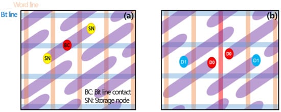
Figure 1.
(a) DRAM cell array diagram and bit line contact and storage node location in DRAM cell. (b) Victim capacitor location according to type of 1-RH.
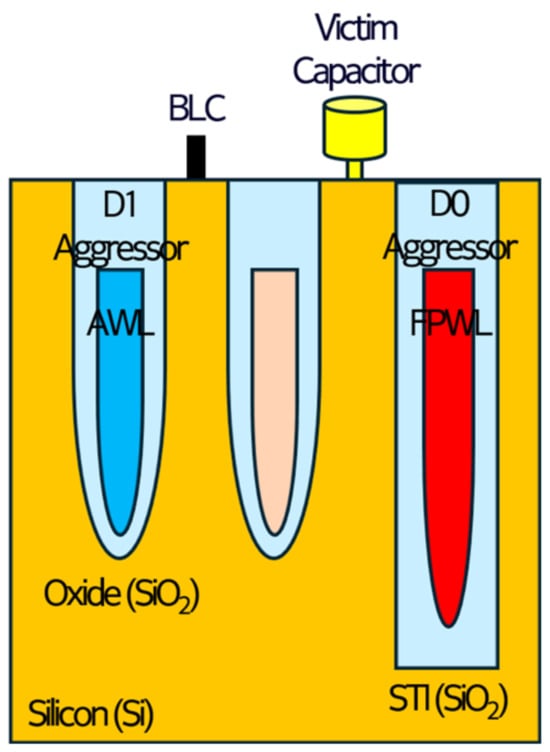
Figure 2.
A 2D cross-sectional view of DRAM cell and locations of aggressor based on types of 1-RH failures.
In this study, we specifically focus on D0 failures within the 1-RH phenomenon, investigating the underlying mechanisms of D0 failure occurrence. Additionally, simulations were conducted based on a buried oxide structure, which has the potential to provide a fundamental solution to mitigating D0 failures. We implemented a buried channel array transistor (BCAT) structure using TCAD 2D simulation to analyze 1-RH phenomena in the mixed mode.
2. 1-Row Hammer
1-RH refers to a phenomenon in which data stored in a capacitor are altered due to the repeated toggling of the aggressor cell within a short period. The types of 1-RH failures can be categorized based on the location of the aggressor, the location where electrons are captured, and the type of data change in the capacitor.
2.1. D1 Failure
As illustrated in Figure 3a, D1 failure occurs when the aggressor is an active word line (AWL). When an AWL is turned on, electrons are collected from its oxide layer. Several of these electrons are captured in the oxide interface traps of the AWL. When the AWL is deactivated, most of the electrons return to a nearby capacitor or BLC. However, the electrons captured in an AWL oxide interface trap can flow to the victim capacitor through diffusion. When this process is repeated, the number of electrons flowing to the victim capacitor increases. Eventually, the data stored as 1 in the victim capacitor change to 0.
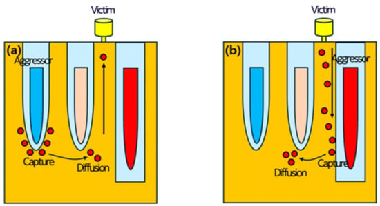
Figure 3.
Electron capture and diffusion in (a) D1 failure and (b) D0 failure. The distinction between D0 and D1 failures lies in the position of the aggressor and the physical distance between the aggressor and the victim capacitor.
2.2. D0 Failure
As illustrated in Figure 3b, D0 failure occurs when the aggressor is an FPWL. When an FPWL is activated, the electrons stored in the victim capacitor gather near the FPWL oxide layer. Several of these electrons are captured in the oxide interface traps of the FPWL. When the FPWL is turned off, most of the electrons return to the victim capacitor. Nevertheless, the electrons captured in an FPWL oxide interface trap can diffuse to the BLC. When the aggressor is repeatedly toggled, the number of electrons diffusing to the BLC increases. Consequently, the voltage of the victim capacitor rises, causing the data to change from 0 to 1.
2.3. Typical Error Bit Correction Methods and Limitations
Irrespective of the specific type of 1-RH failure, the simultaneous occurrence of D1 and D0 results in data loss from the victim capacitor. To mitigate such data loss, DRAM employs periodic refresh operations. However, the presence of 1-RH shortens the refresh interval, thereby degrading DRAM performance. Existing error correction mechanisms for DRAM, such as error correction codes (ECC), static counter assignments, and probabilistic row activation adjustments [,,,,,,,,,,,,,,,], offer only partial remedies. Since 1-RH induced by aggressor attacks generates multi-cell bit errors, rather than isolated single-cell errors, these methods fail to provide a comprehensive solution. Consequently, a more fundamental approach is required to address 1-RH, which poses a significant challenge to current DRAM performance.
3. Simulation Condition
We adopted the 2y nm technology node for DRAM to implement D0 failure. Figure 4 shows a cross-sectional view of a DRAM half-cell. We conducted simulations by implementing a saddle fin structure, which is utilized in the BCAT structure [,,,,,]. In addition, a structure in which 1-RH could be measured was constructed by adding a capacitor. The storage node capacitance was 10 fF. The dimensions of the structure were similar to those of a typical DRAM cell 2y nm technology node. We used the voltage levels within the operating range of a typical DRAM and simulated an environment closely similar to that of the DRAM operation (Table 1). 1-RH was implemented by applying a toggle signal to an FPWL, which acted as an aggressor. To implement the 1-RH in the simulation, we applied a pulse with a 100 ns on/off time and a 10 ns rise/fall time in MixedMode. During the 1-RH, 0.5 V was applied to the drain, −0.3 V to the WLv, and 0 V to the substrate. To evaluate the impact of the 1-RH on the trap properties and structural changes in the device, we measured the average voltage change in the capacitor per pulse. We adopted the following mixed-mode models: (1) doping-dependent Shockley–Read Hall recombination, (2) band-to-band tunneling, (3) continuously variable transmission, (4) Fowler–Nordheim tunneling and direct tunneling, and (5) hot electron injection. This environment is critical for accurately evaluating D0. Based on these structural and voltage conditions, we investigated D0.
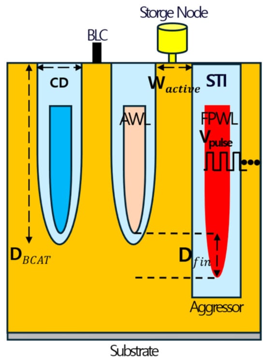
Figure 4.
A 2D cross-sectional view of the BCAT structure implemented by simulation.

Table 1.
BCAT structure, DRAM operating voltage conditions and pulse conditions for implementing D0 failure.
4. 1-Row Hammer Measurement
Before implementing D0 failure, data 0 was stored in the victim capacitor in mixed mode. Figure 5a illustrates the charging voltage of the victim capacitor in response to the toggle signal, which repeats the turn on/off of the FPWL 10 times. We observed a change in the charge voltage over 10 cycles of the toggle signal and extracted the delta voltage from the difference in charge voltage (Figure 5b). The larger the delta voltage, the weaker the structure is against 1-RH attacks. In this study, we used the size of the delta voltage as an indicator of the D0 strength. We investigated the 1-RH tendency of the proposed structure in a D0 failure implementation environment.
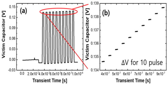
Figure 5.
(a) Charging voltage of the victim capacitor with respect to pulse voltage. (b) Variation in the magnitude of the charging voltage of the victim capacitor during 10 pulse voltages.
5. Baseline Simulation Results and Analysis
The simulation consisted of an investigation of the shallow trench isolation (STI) interface trap of the BCAT structure and an investigation of the structure adopting buried oxides in BCAT. The interface trap investigation focused on 1-RH by changing the density, location, and energy level, and the buried oxide investigation examined the effect on 1-RH by varying the distance, thickness, and length.
5.1. STI with Interface Trap
Figure 6a illustrates the interface trap region at the STI of DRAM. The interface trap was formed close to the victim capacitor to investigate its effect on 1-RH. Figure 6b illustrates the tendency of D0 with respect to the trap location. By dividing the trap location by the area, we found that the deeper the trap location, the stronger the D0 failure. However, if the trap location was deeper than the end of the FPWL, D0 was weakened. The deeper the trap location, the smaller the probability of electrons returning to the victim capacitor after being captured, resulting in a stronger D0. Nevertheless, if the trap location was extremely deep, the effect of the FPWL voltage was reduced in the trap area and few electrons would be captured in the trap, leading to a weaker D0. Figure 7a illustrates the correlation between the trap density and D0. As the trap density increased, the ΔV/pulse tended to increase. Figure 7b illustrates the correlation between the trap energy level and 1-RH. As the trap energy level increased, the ΔV/pulse increased. Both the trap density and energy level affected electron capturing during the 1-RH phenomenon. The higher the trap density, the greater the number of electrons from the victim capacitor captured in the interface trap. Additionally, electrons cannot easily be discharged when they are captured at high trap energy levels. If numerous electrons are captured in the trap or remain captured, the probability that D0 will occur is high because these electrons will not return to the victim capacitor. These results demonstrated that D0 failures occurred sensitively depending on the density and energy level of traps on the STI surface. The process results demonstrated that the trap density on the STI surface was closely related to the STI process and was determined by the STI film quality. To suppress D0 failure, the interfacial trap density should be reduced by improving the STI quality.
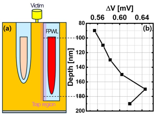
Figure 6.
(a) Location of trap region in BCAT structure. (b) Correlation between trap region location and delta V.
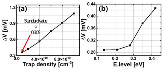
Figure 7.
(a) Tendency of D0 with trap density. (b) Delta voltage with respect to the width variation in energy level.
5.2. Device Structure
Next, we conducted a detailed analysis of the simulation results for the device structure. As shown in Figure 8a, an increase in the fin depth amplifies its effect, whereas Figure 8b demonstrates that a reduction in the active width enhances the observed impact. Regarding fin depth, similar to the trap region, a greater depth reduces the likelihood of electrons returning to the capacitor during the diffusion process. Conversely, an increase in the active width enlarges the SN node area, thereby increasing the probability of electrons returning to the capacitor. The simulation results reveal how both device structure and trap characteristics influence the capture and diffusion processes associated with D0 failure.
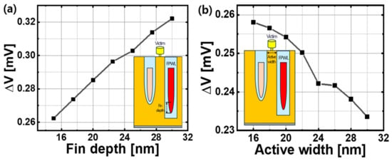
Figure 8.
The simulation result of D0 failure according to device structure: (a) results of fin depth; (b) results of active width.
In summary, traps predominantly affect the electron capture process, while the device structure governs the diffusion mechanism. Based on these findings, three potential approaches to mitigating D0 failure are suggested: the first is reducing the number of trapped electrons by improving the oxide film quality; the second is enhancing the probability of electrons returning to the capacitor through the structural modification of the device; and the third is mitigating electron movement by the FPWL.
6. Buried Oxide Simulation Results and Analysis
We propose a method for fabricating the buried oxide structure by growing silicon through epitaxial growth. The steps involved in the buried oxide process are illustrated in Figure 9. Figure 9a depicts the deposition of an oxide layer onto a silicon wafer. In Figure 9, the oxide layer is patterned and etched to define the regions that will form the buried oxide. Figure 9c shows the epitaxial growth of silicon adjacent to the etched oxide. Finally, Figure 9d illustrates the completed buried oxide structure following the silicon epitaxial growth.

Figure 9.
The process steps of buried oxide. (a) Silicon wafer with oxide layer. (b) Oxide after pattering and etching. (c) Growing silicon through epitaxial growth. (d) Buried oxide structure after process.
Figure 10a shows the buried oxide region under the AWL oxide. We investigated the tendency of D0 in terms of the distance, width, and thickness of the buried oxide. Figure 10b illustrates the tendency of D0 with respect to the buried oxide and AWL oxide distance. The closer the buried oxide was to the AWL oxide, the weaker the D0 effect. The distance between the buried and AWL oxides affected diffusion during the D0 process. The closer the distance, the more effectively the captured electrons were physically prevented from flowing to the BLC. In other words, the captured electrons could return to the victim capacitor. Figure 11a illustrates the correlation between the buried oxide and D0. D0 was strongly proportional to the thickness of the buried oxide. As the thickness of the buried oxide layer increased, the potential of the substrate decreased, thereby reducing the influence of the substrate voltage on the channel. As a result, when the influence of the electric field generated by the substrate voltage on the AWL channel decreased, the probability of the captured electrons diffusing toward the BLC increased. Figure 11b illustrates the relationship between D0 and the width of the buried oxide. We confirmed that the delta voltage decreased with the width of the buried oxide layer and then increased again. In other words, the optimal width of the buried oxide layer for alleviating D0 failure was identified using the simulation results. The variation in the width of the buried oxide layer affected both the capture and diffusion processes of D0. If the buried oxide layer is thin, electron diffusion cannot be sufficiently suppressed. When the buried oxide layer does not have sufficient width, electron diffusion cannot easily be prevented physically (Figure 12b). Conversely, if the width of the buried oxide layer exceeds a certain threshold, electron capturing cannot be sufficiently mitigated. When the width of the buried oxide layer exceeds a certain level, the effect of the electric field on the silicon active area owing to the substrate voltage decreases. This increases the number of electrons from the victim capacitor trapped in the interface trap (Figure 13b). Consequently, the adoption of buried oxides reduces D0 failure. Optimizing the distance, thickness, and width of the buried oxide layer is crucial for mitigating D0.
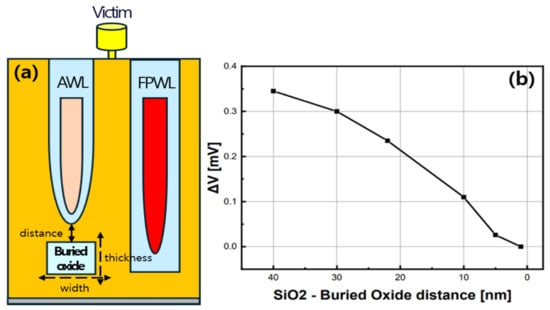
Figure 10.
(a) BCAT structure with buried oxide added. (b) Tendency of D0 with buried oxide distance.
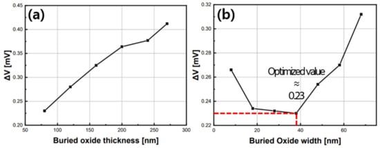
Figure 11.
(a) Delta voltage against the thickness variation in buried oxide layer. (b) Delta voltage against width variation in buried oxide layer.
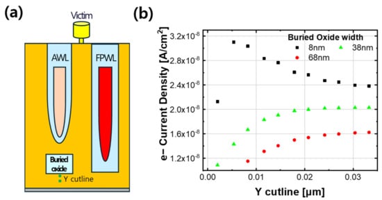
Figure 12.
(a) Diagram presenting the y-cutline position to show the e-current density area within the BCAT. (b) Diagram showing the current density of electrons flowing down the buried oxide.
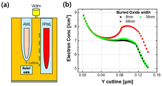
Figure 13.
(a) Diagram presenting the y-cutline position to show the electron concentration area within the BCAT. (b) Diagram showing the concentration of electrons flowing next to the STI.
7. Conclusions
In this study, we investigated the occurrence locations and mechanisms of two types of 1-RH failures: D1 and D0. 1-RH consists of two processes: the capture and diffusion of electrons. We analyzed D0, which occurs more frequently than D1 in the current DRAM structure. D0 failure was analyzed by investigating the impact on the interface trap and structure adopting buried oxides. The results demonstrated that the interface trap was closely related to the electron capture process, which was influenced by the density and energy levels of the interface trap. To effectively reduce D0, the membrane quality of the STI should be improved, and the trap density should be reduced. The structure of the buried oxide affected both the capture and diffusion processes of electrons. We found that the closer the buried oxide position was to the AWL channel and the thinner the thickness of the oxide layer, the less D0 occurred when the layer had an appropriate width. We demonstrated that D0 could be reduced by optimizing the buried oxide layer and therefore adopted a buried oxide structure rather than the existing BCAT structure, resulting in a 25% reduction in D0. Finally, we analyzed the limitations of error-bit correction and concluded that a fundamental solution was required. As a fundamental solution, we investigated the suppression of D0 failures using structural engineering. Our study demonstrates that structures that adopt buried oxides can effectively reduce D0.
Future research should focus on examining the sensitivity of buried oxide interface traps to 1-RH. Since the interface traps in shallow trench isolation (STI) have been shown to significantly influence the 1-RH phenomenon, it is expected that interface traps in buried oxide will similarly play a crucial role. Moreover, forthcoming studies indicate that structural modifications offer a fundamental solution to mitigating 1-RH. Thus, proposing alternative DRAM cell structures and systematically analyzing the impact of these designs on 1-RH behavior will be a critical focus of future work.
Author Contributions
Conceptualization, M.-W.K.; Software, Y.-S.K.; Validation, M.-W.K.; Investigation, Y.-S.K. and M.-W.K.; Writing—original draft, Y.-S.K.; Writing—review & editing, M.-W.K. All authors have read and agreed to the published version of the manuscript.
Funding
This research was supported by the National R&D Program through the National Research Foundation of Korea (NRF), funded by the Ministry of Science and ICT (NRF-2022M3I7A1078936) and this research was supported by “Regional Innovation Strategy (RIS)” through the National Research Foundation of Korea (NRF) funded by the Ministry of Education (MOE) (2022RIS-005).
Data Availability Statement
Data are contained within the article.
Conflicts of Interest
The authors declare no conflict of interest.
References
- Lim, C.-Y.; Kim, Y.-S.; Kwon, M.-W. Interfacial Trap-based 1-row Hammer Analysis of BCAT and Nitride Layer BCAT Structures in Dynamic Random Access Memory. J. Semicond. Technol. Sci. 2024, 24, 18–24. [Google Scholar]
- Kim, Y.-S.; Lim, C.-Y.; Kwon, M.-W. Mitigating WL-to-WL Disturbance in Dynamic Random-Access Memory (DRAM) through Adopted Spherical Shallow Trench Isolation with Silicon Nitride Layer in the Buried Channel Array Transistor (BCAT). Electronics 2024, 13, 681. [Google Scholar] [CrossRef]
- Sun, Y.; Liu, X.; Wang, N.; Jeon, J.; Wu, B.; Cao, K. Trap-assisted passing word line leakage and variable retention time in DRAM. In Proceedings of the 2021 IEEE 4th International Conference on Electronics Technology (ICET), Chengdu, China, 7–10 May 2021. [Google Scholar]
- Gautam, S.K.; Manhas, S.K.; Kumar, A.; Pakala, M. Mitigating the passing word line induced soft errors in saddle fin DRAM. IEEE Trans. Electron Devices 2020, 67, 1902–1905. [Google Scholar] [CrossRef]
- Son, M.; Park, H.; Ahn, J.; Yoo, S. Making DRAM stronger against row hammering. In Proceedings of the 54th Annual Design Automation Conference, Austin, TX, USA, 18–22 June 2017. [Google Scholar]
- Yang, T.; Lin, X.-W. Trap-assisted DRAM row hammer effect. IEEE Electron Device Lett. 2019, 40, 391–394. [Google Scholar] [CrossRef]
- Peng, X.; Abshire, P. Stochastic Behavior of a CMOS Inverter. In Proceedings of the 2007 14th IEEE International Conference on Electronics, Circuits and Systems, ICECS 2007, Marrakech, Morocco, 11–14 December 2007; pp. 94–97. [Google Scholar]
- Yağlıkçı, A.G.; Luo, H.; de Oliviera, G.F.; Olgun, A.; Patel, M.; Park, J.; Hassan, H.; Kim, J.S.; Orosa, L.; Mutlu, O. Understanding rowhammer under reduced wordline voltage: An experimental study using real dram devices. In Proceedings of the 2022 52nd Annual IEEE/IFIP International Conference on Dependable Systems and Networks (DSN), Baltimore, MD, USA, 27–30 June 2022. [Google Scholar]
- Cojocar, L.; Razavi, K.; Giuffrida, C.; Bos, H. Exploiting correcting codes: On the effectiveness of ECC memory against Rowhammer attacks. In Proceedings of the 2019 IEEE Symposium on Security and Privacy (SP), San Francisco, CA, USA, 19–23 May 2019; pp. 55–71. [Google Scholar] [CrossRef]
- Yinyi, L.; Wolf, J.K. Combined ECC/RLL code. IEEE Trans. Magn. 1998, 24, 2527–2529. [Google Scholar] [CrossRef]
- Hong, S.; Kim, D.; Lee, J.; Oh, R.; Yoo, C.; Hwang, S.; Lee, J. Dsac: Low-cost rowhammer mitigation using in-dram stochastic and approximate counting algorithm. arXiv 2023, arXiv:2302.03591. [Google Scholar]
- Luo, H.; Olgun, A.; Yağlıkçı, A.G.; Tuğrul, Y.C.; Rhyner, S.; Cavlak, M.B.; Lindegger, J.; Sadrosadati, M.; Mutlu, O. Rowpress: Amplifying read disturbance in modern dram chips. In Proceedings of the 50th Annual International Symposium on Computer Architecture, Orlando, FL, USA, 17–21 June 2023. [Google Scholar]
- Kim, J.S.; Patel, M.; Yaglikci, A.G.; Hassan, H.; Azizi, R.; Orosa, L.; Mutlu, O. Revisiting Rowhammer: An experimental analysis of modern dram devices and mitigation techniques. In Proceedings of the 2020 ACM/IEEE 47th Annual International Symposium on Computer Architecture (ISCA), Valencia, Spain, 30 May–3 June 2020. [Google Scholar]
- Patel, M.; Kim, J.S.; Hassan, H.; Mutlu, O. Understanding and modeling on-die error correction in modern DRAM: An experimental study using real devices. In Proceedings of the 2019 49th Annual IEEE/IFIP International Conference on Dependable Systems and Networks (DSN), Portland, OR, USA, 24–27 June 2019. [Google Scholar]
- Lin, C.-H.; Shen, D.-Y.; Chen, Y.-J.; Yang, C.-L.; Wang, M. SECRET: Selective error correction for refresh energy reduction in DRAMs. In Proceedings of the 2012 IEEE 30th International Conference on Computer Design (ICCD), Montreal, QC, Canada, 30 September–3 October 2012. [Google Scholar]
- Chen, H.-M.; Jeloka, S.; Arunkumar, A.; Blaauw, D.; Wu, C.-J.; Mudge, T.; Chakrabarti, C. Using low cost erasure and error correction schemes to improve reliability of commodity DRAM systems. IEEE Trans. Comput. 2016, 65, 3766–3779. [Google Scholar] [CrossRef]
- Pae, S.-I.; Kozhikkottu, V.; Somasekar, D.; Wu, W.; Ramasubramanian, S.G.; Dadual, M.; Cho, H.; Kwon, K.-W. Minimal aliasing single-error-correction codes for dram reliability improvement. IEEE Access 2021, 9, 29862–29869. [Google Scholar] [CrossRef]
- Seyedzadeh, S.M.; Jones, A.K.; Melhem, R. Counter-based tree structure for row hammering mitigation in DRAM. IEEE Comput. Archit. Lett. 2016, 16, 18–21. [Google Scholar] [CrossRef]
- Kim, D.-H.; Nair, P.J.; Qureshi, M.K. Architectural support for mitigating row hammering in DRAM memories. IEEE Comput. Arch. Lett. 2014, 14, 9–12. [Google Scholar] [CrossRef]
- Kim, Y.; Daly, R.; Kim, J.; Fallin, C.; Lee, J.H.; Lee, D.; Wilkerson, C.; Lai, K.; Mutlu, O. Flipping bits in memory without accessing them: An experimental study of DRAM disturbance errors. ACM SIGARCH Comput. Archit. News 2014, 42, 361–372. [Google Scholar] [CrossRef]
- Bostanci, F.N.; Yüksel, I.E.; Olgun, A.; Kanellopoulos, K.; Tuğrul, Y.C.; Yağliçi, A.G.; Sadrosadati, M.; Mutlu, O. CoMeT: Count-Min-Sketch-based Row Tracking to Mitigate RowHammer at Low Cost. In Proceedings of the 2024 IEEE International Symposium on High-Performance Computer Architecture (HPCA), Edinburgh, UK, 2–6 March 2024. [Google Scholar]
- Woo, J.; Chung, K.S. Mitigating Row-hammering by Adapting the Probability of Additional Row Refresh. In Proceedings of the 2019 IEEE 4th International Conference on Technology, Informatics, Management, Engineering & Environment (TIME-E), Bali, Indonesia, 13–15 November 2019. [Google Scholar]
- Park, S.W.; Hong, S.J.; Kim, J.W.; Jeong, J.G.; Yoo, K.D.; Moon, S.C.; Sohn, H.C.; Kwak, N.J.; Cho, Y.S.; Baek, S.J.; et al. Highly scalable saddle-Fin (S-Fin) transistor for sub-50nm DRAM technology. In Proceedings of the 2006 Symposium on VLSI Technology, Digest of Technical Papers, Honolulu, HI, USA, 13–15 June 2006. [Google Scholar]
- Han, J.-W.; Suh, M.; Lee, G.; Kim, J. Overhang saddle fin sidewall structure for highly reliable DRAM operation. IEEE Access 2023, 11, 82738–82743. [Google Scholar] [CrossRef]
- Gautam, S.K.; Manhas, S.K.; Kumar, A.; Pakala, M.; Yieh, E. Row hammering mitigation using metal nanowire in saddle fin DRAM. IEEE Trans. Electron Devices 2019, 66, 4170–4175. [Google Scholar] [CrossRef]
- Liu, X.; Sun, Y.; Wang, N.; Jeon, J.; Wu, B.; Cao, K. Saddle Fin Structure Effects on the DRAM Access Transistor Performance. In Proceedings of the 2021 IEEE 4th International Conference on Electronics Technology (ICET), Chengdu, China, 7–10 May 2021. [Google Scholar]
- Kim, Y.K.; Lee, J.S.; Kim, G.; Park, T.; Kim, H.J.; Cho, Y.P.; Park, Y.J.; Lee, M.J. Partial isolation type saddle-FinFET (Pi-FinFET) for sub-30 nm DRAM cell transistors. Electronics 2019, 8, 8. [Google Scholar] [CrossRef]
- Liu, X.; Sun, Y.; Li, D.; Jeon, J.; Wu, B. TCAD Simulation on Saddle-Fin Device Performance Boosting with Word Line Engineering. In Proceedings of the 2023 6th International Conference on Electronics Technology (ICET), Chengdu, China, 12–15 May 2023. [Google Scholar]
Disclaimer/Publisher’s Note: The statements, opinions and data contained in all publications are solely those of the individual author(s) and contributor(s) and not of MDPI and/or the editor(s). MDPI and/or the editor(s) disclaim responsibility for any injury to people or property resulting from any ideas, methods, instructions or products referred to in the content. |
© 2024 by the authors. Licensee MDPI, Basel, Switzerland. This article is an open access article distributed under the terms and conditions of the Creative Commons Attribution (CC BY) license (https://creativecommons.org/licenses/by/4.0/).