Article

Ultrathin Antenna-in-Package Based on TMV-Embedded FOWLP for 5G mm-Wave Applications

1
The 58th Research Institute of China Electronics Technology Group Corporation, Wuxi 214035, China
2
School of Electronic Science & Engineering, Southeast University, Wuxi 214111, China
3
School of Electronic Science and Engineering, University of Electronic Science and Technology of China (UESTC), Chengdu 611731, China
*
Author to whom correspondence should be addressed.
Electronics 2024, 13(5), 839; https://doi.org/10.3390/electronics13050839
Submission received: 11 January 2024 / Revised: 1 February 2024 / Accepted: 4 February 2024 / Published: 22 February 2024

Abstract

:
In this paper, a novel through mold via (TMV)-embedded fan-out wafer-level package (FOWLP) technology was demonstrated to manufacture the well-designed Antenna in Package (AiP) with ultrathin thickness (0.04 λ0). Double-sided redistribution layers (RDLs) were employed to build the patch antenna, while a TMV interposer was used to connect the front and back RDLs. By optimizing the AiP’s parameters, the patch antenna can achieve a wide impedance bandwidth of 17.8% from 24.2 to 28.5 GHz, which can cover the 5G frequency bands. Compared with previous works, the proposed AiP has significant benefits in terms of its ultralow profile, easy processing, and high gain. Hence, the TMV-embedded FOWLP should be a promising technology for fifth generation (5G) millimeter wave (mm-Wave) applications.

1. Introduction

Wireless communication has witnessed an explosive expansion over the past decade. The remarkable advancement in diverse emerging fields such as virtual reality (VR), artificial intelligence (AI), and the Internet of Things (IoT) has generated an immense surge in data traffic [1]. Therefore, the current demand called for systems capable of delivering high data rates, wide bandwidth, and low latency. Meanwhile, there was an increasing demand for portable equipment that was easy to carry and did not occupy much space in those emerging applications. In addition, cost-effectiveness was also crucial to ensure that these devices were affordable and accessible for purchase and used by a wide range of users. As a result, the handheld devices connected to these systems should be compact and cost-effective.
Due to the strong demand for high-quality communication and high-integration devices, there has been considerable attention drawn to the fifth-generation communication (5G) in the millimeter-Wave (mm-Wave) bands. Mm-Wave communications offer several advantages over existing wireless technologies, including an extensive bandwidth, compact component sizes, and narrow beams, which can break the limitations of frequency spectrum availability in the sub-6 GHz bands. Hence, mm-Wave systems are spreading widely into mainstream communication terminal devices in wireless communication [2]. Moreover, with the increase in the density of 5G, it can support the increasing demand for smart city infrastructure. Fifth-generation networks were engineered to provide enhanced reliability, lower latency, and improved network efficiency, making them ideal for critical applications such as autonomous vehicles, telemedicine, and industrial automation. As a result, these unique characteristics of 5G have garnered considerable attention and stimulated innovation in various industries, driving the global adoption and deployment of 5G technologies worldwide.
The third-generation partnership project (3GPP) states that the mm-Wave bands adopted for 5G communication cover the following frequency ranges: 24.25–27.50 GHz (n258), 26.5–29.5 GHz (n257), 27.50–28.35 GHz (n261), 37.0–40.0 GHz (n260), 39.5–43.5 GHz (n259), and 47.2–48.2 GHz (n262) [3]. Therefore, designing wideband antennas that cover multiple mm-Wave 5G frequency bands was a significant challenge in meeting different standards worldwide. Meanwhile, it was recommended to adopt miniaturization and low-profile technology for 5G antennas in terminal devices due to the limited internal space. In addition, the use of 5G mm-Wave presented a constant challenge due to high path and transmission losses at high frequencies, which result in a requirement in high gain and high efficiency of the antenna [4].
To meet the above requirements, the design and fabrication of 5G mm-wave antennas played a significant role. Mm-wave antennas can be fabricated in either integrated or non-integrated structures depending on the specific application and requirements. The non-integrated antennas were structured that were separate from the electronic circuitry and come in various forms. Integrated antennas were designed to be integrated directly into a circuit board or within a larger electronic system, including antenna-on-chip (AoC) and antenna-in-package (AiP) systems. These integrated designs offered compact solutions that enable antennas to be integrated into electronic devices, enhancing their performance and functionality. However, achieving high efficiency in AoC designs was challenging due to the low resistivity and high permittivity of the silicon substrate [5]. The use of silicon substrates for integrated circuit fabrication imposed inherent limitations on the antenna’s performance. The low resistivity of the silicon led to increased conduction losses, which can reduce the overall efficiency of the antenna. Losses can be caused by the substrate absorbing and dissipating a significant portion of the radiated energy. Additionally, the high dielectric constant of silicon can cause an impedance mismatch and distort the radiation pattern of the antenna.
Hence, AiP was considered excellent candidates in industry and academia for integrating the antenna with the chip to reduce interconnect length. Furthermore, integrating the antenna within the package allowed for tighter coupling and better impedance matching between the antenna and the RF chip, resulting in improved transmission efficiency, reduced power consumption, and an enhanced overall system performance [6].
State-of-the-art mm-Wave package technologies to achieve AiP included a low-cost printed circuit board (PCB) [7,8,9], low temperature co-fired ceramic (LTCC) [10,11], high-density interconnection (HDI) [12,13], and fan-out wafer-level package (FOWLP) [14,15,16], respectively. LTCC technology has gained significant traction in the fabrication of AiP structures for 5G applications due to its ability to provide substrates with low loss, minimal moisture absorption, excellent thermal conductivity, and a high degree of passive component integration [17]. LTCC devices were manufactured using ceramic tapes and metal pastes. This technology facilitated manufacturing services to promote mass production. However, the main challenges faced by LTCC technology were the limitations of manufacturing process accuracy and the associated high costs [18]. HDI technologies allowed for the simultaneous use of a variety of dielectric materials, with single layer thicknesses ranging from 10 to 100 μm, providing unparalleled design flexibility. Additionally, HDI technologies enabled the use of blind and buried vias by developing an accumulation layer on a rigid core substrate, which can facilitate complex signal routing [19]. However, this approach typically involved complex structures and multilayers.
Compared to LTCC or HDI technologies, FOWLP utilized a wafer reconstruction process. This involved selecting functional dies from the original device wafer, placing them onto a carrier, and encapsulating them with epoxy molding compound (EMC) to form an artificial wafer. This innovative approach eliminated the need for a laminate substrate and instead utilized Cu redistribution layers (RDLs) [20].
Among these aforementioned technologies, FOWLP emerged as an impressive candidate in AiP due to its low structure profile, compact size, and high I/O density [21]. FOWLP eliminated the need for traditional wire bonding or flip chip interconnects, enabling more direct and compact integration of the antenna and RF chip. This consequence resulted in a reduced package size and overall profile, which is particularly beneficial for applications with tight space constraints. Additionally, the technology enabled the redistribution of the I/Os across the entire surface of the package, resulting in a higher number of connections and denser integration of antennas and RF chips. Furthermore, FOWLP offered an exceptional thermal and electrical performance. The RDL in FOWLP provided a short interconnect length and low parasitic effects, resulting in improved signal integrity, reduced losses, and the enhanced performance of the integrated antenna and RF chip.
Recently, several reports have been illustrated to AiP element designs and research for 5G applications, using FOWLP technology. In [16,22,23], new configurations of AiPs based on FOWLP technology were introduced in response to emerging wireless communications. In [22], a patch antenna with a gain of approximately 5 dBi and bandwidth of around 5.7 GHz at 28 GHz was implemented in the FOWLP package for 5G mm-Wave applications. In [23], a dual-band slotted patch antenna was designed for 28 GHz/38 GHz 5G small cell base stations with a gain of about 6.2 dBi. These configurations offered several advantages. FOWLP technology minimized the thickness of the package, reduced the length of the signal path between the antenna and the chip, enabled integration of the antenna on top of the chip, allowed for package size reduction, and enabled easy scalability, with larger arrays and multiple chips. However, these designs cannot satisfy all the needs, including a low profile, fewer layers, and high gain, simultaneously.
TMV-embedded FOWLP has been illustrated as an outstanding approach for achieving highly integrated packages due to its ability to reduce interconnection loss, improve signal isolation, and achieve fine pitch line and spaces. Figure 1 shows an example of a TMV-embedded FOWLP. The chip-to-package interconnected in the TMV-embedded FOWLP was developed through the TMV interposer that lands directly onto the chip from the RDL. Large-scale antennas integrated with various RF chips in the same package have been identified as an exceptional approach for mm-Wave communication modules. Therefore, TMV-embedded FOWLP has become one of the most promising candidates for mm-Wave communications due to its support for embedded chips and low-loss interconnects.
In this work, a novel FOWLP technology with double-sided RDLs, particularly TMV interposers as a vertical interconnect, was illustrated. For the patch element design, the parasitic patches were employed to further widen bandwidth. The low-cost FOWLP process, which included picked and placed, molding, seed layer deposition, photoresist patterning, electroplating, and grinding, was selected for the fabrication. The AiP, based on FOWLP technology with a low profile and fewer layers, was designed and fabricated for 5G mm-Wave applications. The simulation and measurement results stated that the antenna achieved a wide impedance bandwidth, high gains, and a good radiation performance, covering the 5G communication frequency bands of n258, n257, and n261.

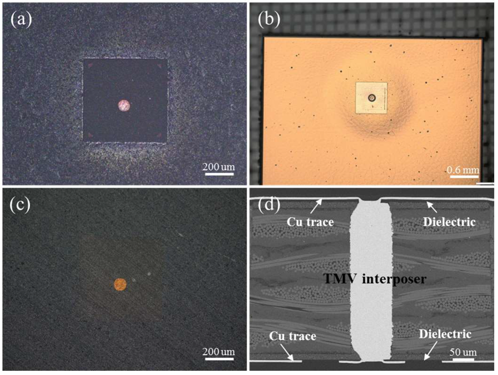
2. Process of TMV-Embedded FOWLP

The fabrication process for the TMV-embedded FOWLP is illustrated in Figure 2. Firstly, a release layer was coated onto the carrier (Figure 2a), and then the chip and TMV interposer were picked and placed on to the release layer (Figure 2b). After that, the whole reconstituted wafer was molded with liquid epoxy material, using the thermal compression approach. The post-mold curing process was conducted after molding (Figure 2c). Next, the carrier was de-bonded from the reconstructed wafer, and the chip and TMV interposers were embedded in the molding compound. The proposed module was equipped with RDLs on both sides of the package.
The fabrication of the front-side RDL began with the application of a dielectric layer on the reconstructed wafer, followed by the formation of RDL layers, using a semi-additive process, which involved depositing a seed layer, patterning with photoresist, electroplating, stripping the photoresist, and etching the seed layer (Figure 2d). Thin wafer handling was critical to achieving the required thickness of the reconfigured wafer; a thick carrier was used as the support wafer (Figure 2e) and then bonded to the front side to protect the RDLs and reduce the warpage of the thin wafer. After completing the back side dielectric layer and RDL (Figure 2f), the carrier wafer was deboned, and the solder balls were attached (Figure 2g). Finally, the reconstituted wafer was diced into individual packages (Figure 2h).
The vertical interconnection structure played an irreplaceable role in allowing the signal/control needs to access from the top RDL to the bottom RDL, and this was due to its advantages of improving integration and fast transmission rates. The interconnect structure allowed signals to pass through multiple layers vertically, facilitating efficient use of the available package area. This enabled a higher integration density and the accommodation of complex routing requirements, even in compact form factors. Connecting the top and bottom RDLs directly shortened the signal paths, resulting in reduced propagation delays and improved signal transmission rates. This was particularly important for high-speed communication and high-frequency applications, where minimizing signal delays was critical for maintaining signal integrity and achieving optimal performance.
At present, various types of vertical interconnections have been developed successfully, including through silicon via (TSV), through glass via (TGV), and through mold via (TMV). TSV structures have significant advantages in semiconductors, and CMOSs in image sensors [24]. However, TSV suffers from low material compatibility and high process costs. On the other hand, TGV structures offered greater advantages in terms of radio frequency and microwave transmission, but their material processing capabilities were limited [25]. Therefore, TMVs have gained significant attention due to their simple fabrication process, low cost, and excellent applicability.
In this project, TMV interposers were implemented to realize the vertical interconnection. Currently, there are several methods available to prepare TMV for integrated circuit packaging, such as laser etching [26], Cu pillar [27], wire bonding [28], and the imprint method [29]. In [26], the TMV was created by laser etching through the embedding molding compound and then metalized via Cu plating. This technique enabled 3D interconnections in multi-chip system in package (SiP) module stacks. The SiP module comprised a stack of multiple sensors, including a pressure sensor and an acceleration sensor, as well as an application-specific integrated circuit (ASIC) package with TMVs. It was specifically designed for a multi-sensor device for indoor navigation. In [27], The TMV was produced using the Cu pillar technique, which involved depositing copper metallization in the developed area of the photoresist. The unique feature of the tall Cu pillar allowed for the design of AiP to satisfy the wide bandwidth characteristic, making it ideal for highly integrated 5G mm-Wave scenarios. In [21], TMV was created using wire bonding, which was evaluated for an ultra-thin package-on-package (PoP) application. The use of vertical Cu wire bonding was cost-effective, as it eliminates many process steps, such as a thick PR coating and Cu plating. In [28], A proposed process called Imprint-Through Mold Via (i-TMV) involved imprinting with a silicon master and filling with conductive paste. The i-TMV has shown its Electromagnetic Interference (EMI) shielding effect through electric field simulation, making it a promising option for compartmental level EMI shielding of radio frequency modules.
In contrast to the abovementioned methods and other works in the literature [29,30], the TMV interposers were fabricated using a mechanical drilling and electroplating process, which has significant benefits in terms of fewer steps and lower cost. Vias were manufactured using mechanical drilling on a glass fiber board with a thickness of 400 μm. The diameter of the vias was 120 μm, with a spacing of 250 μm. The vias were filled using the electroplating process, resulting in a 12-inch core board. To ensure the stability and usability of the core board during the packaging process, resin materials were applied to protect both sides of the core board, attaining a TMV interposer.
As shown in Figure 3a, the 1 × 1 TMV interposer array was selected, with a copper column with a diameter of 120 μm and without surface anomalies. It was important to note that the TMV interposer can be produced in different sizes and arrays by adjusting the diameter and spacing of vias to satisfy various requirements. The Cu RDL was implemented on the TMV interposer side of the reconstructed wafer. The passivation layer was accomplished using photoresist materials, and Cu redistribution traces were created through a seed layer deposition and electroplating process. The processes were optimized for fine-pitch RDL, resulting in good coverage, without damaging the RDL (Figure 3b).
In order to protect the front-side RDLs and minimize the warpage of the thin wafer, a thick carrier was employed as a support wafer before thinning. The reconfigured wafer was thinned to 450 μm, exposing Cu pillar of the TMV interposer on the back side, as shown in Figure 3c. The diameter of the exhibited Cu pillar was 120 ± 3 μm, consistent with the result of the front-side Cu pillar. The results indicated that the Cu pillars in the TMV interposer were uniform. After debonding from the carrier wafer, solder balls were attached. The reconstituted wafer was then diced into individual packages. A cross-section analysis demonstrated that the copper trace was electroplated over the dielectric via an opening on the Cu TMV. The integrity of the TMV interposer with the top and bottom RDL was also confirmed, as shown in Figure 3d.

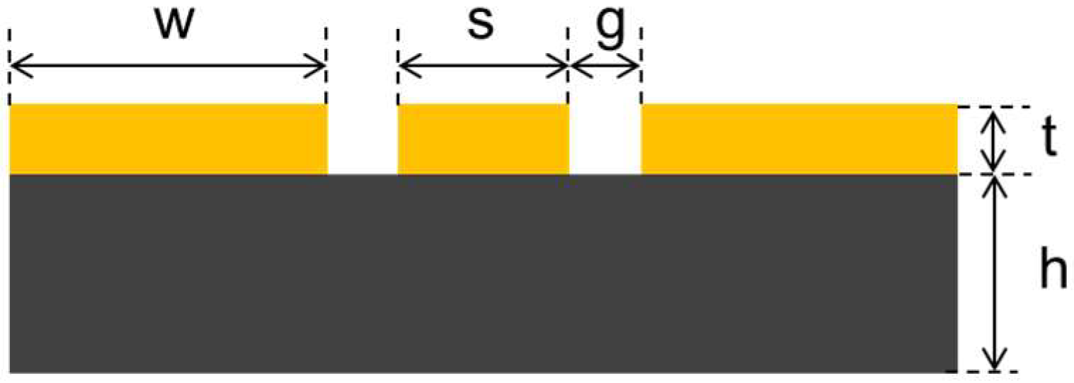
3. Antenna-in-Package Design

To design the AiP solution effectively, it was crucial to have a comprehensive understanding of the electrical properties of the EMC used in the mm-Wave band. The performance of AiP was significantly influenced by the relative permittivity and loss tangent of the applied material. Consequently, a CPW structure was devised to derive these properties. Figure 4 presents a top view of the CPW structure, featuring five parameters: the width (w) of the metal electrodes on both sides, the spacing (g) between the electrode and the middle signal line, the width (s) of the signal line, the thickness (t) of the metal electrode, and the thickness (h) of the substrate., The design parameters were optimized to be w = 1 mm, g = 0.03 mm, s = 0.26 mm, t = 0.005 mm, and h = 0.7 mm based on actual process parameters and simulation results. The structure of CPW was measured using ground–signal–ground (GSG) probes. The material parameters (εr, tanδ) of the EMC were attained by measuring the S-parameters and applying a calculation formula. To ensure greater accuracy, transmission lines of different length were manufactured for testing, resulting in the following average values: εr = 3.93 ± 0.1 and tanδ = 0.006 ± 0.002 at 28 GHz. These data will support subsequent electrical simulations.
FOWLP technology has been extensively validated as an effective solution for mm-Wave applications. Figure 5 illustrates the architecture of designed AiP, which was composed of a TMV interposer, EMC, and double-sided RDLs sandwiching the mold compound. The proposed patch antenna was fabricated on the EMC substrate with a thickness of 0.04 λ0. The dielectric and RDL layers were established on dual sides of the EMC. The top RDL was designed for the active antenna patch and parasitic patch antenna, while the bottom RDL served as the ground plane (GND). The TMV interposer was employed to route the interconnections between the patch and GND.
In particular, Figure 5c described the geometry of the proposed antenna. It consisted of three components: a main radiating patch, six metallic parasitic patches symmetrically placed along with the main radiating patch on the top layer, and a ground plane on the bottom layer. The size of the main radiating patch was L1 × W1. The size of all parasitic square patches was equivalent with a. The gap between parasitic square patches was b, the range between parasitic patches and main radiating patch was c, and the diameter of Cu via was d.
Patch antennas were extensively utilized in various fields, including satellite communication and environmental detection, due to their compact size, thin profile, simple manufacturing process, low cost, ease of integration, and ability to support dual-band and multi-band operations. However, the development of the patch antenna was hindered by its relatively narrow impedance bandwidth. A wide range of research works have been conducted to broaden the bandwidth of patch antennas. These studies investigated different techniques, including increasing the thickness of dielectric substrates, incorporating parasitic patches, and employing coupling feeding [31].
In this study, six metallic parasitic patches were developed to expand the bandwidth. By loading these parasitic patches in the particular manners, a new resonant frequency of the patch antenna was excited, resulting in a wider operational bandwidth [32]. In order to verify the above research conclusion, a single patch antenna with the same size and feeding way is given for a comparison. The simulated |S11| of the patch antenna with and without the symmetrical parasitic patches is plotted in Figure 6. The introduction of these parasitic patches results in a wider impedance bandwidth, ranging from 24.2 to 28.5 GHz.
In order to analyze the main factors of fabrication in TMV-embedded FOWLP technologies and evaluate the electrical performance of antenna, the effects of various geometrical parameters, such as the TMV height and TMV size, were investigated. The parameters for the patch antenna design in Figure 7 are presented in Table 1. Figure 7a shows the return loss characteristics under different values of TMV height. It can be observed that when the TMV height increased, the first and second resonant frequencies of each antenna were shifted down simultaneously. In addition, when the height increased to 300 μm, the two resonances became further separated, but the resulting input matching worsens. Figure 7b revealed the effect of the TMV size on the return loss. With the antenna height increased, the first resonant frequencies were rarely changed, while the second resonant frequencies shifted toward a lower frequency region, leading to a narrower bandwidth. During the fabrication procedure, it was likely necessary to take the misalignment effect and restriction into account. Thus, the TMV height and TMV size chosen were set at 300 μm and 0.6 × 0.6 mm2, separately.
The impact of the constitutive parameters of the parasitic patch structure on the bandwidth was investigated. Figure 8 demonstrated the variation trend of |S11|, which was substantially impacted by the parameters of the parasitic patch structure. As demonstrated in Figure 8, with the increase in a, the lower resonant frequencies were different, while the significant decrease in higher resonant frequencies resulted in a narrower operating bandwidth, but the impedance matching was improved. With the increase in c, the dramatically increased lower resonant frequency, together with the slightly decreased higher resonant frequency, led to a wider operating bandwidth.

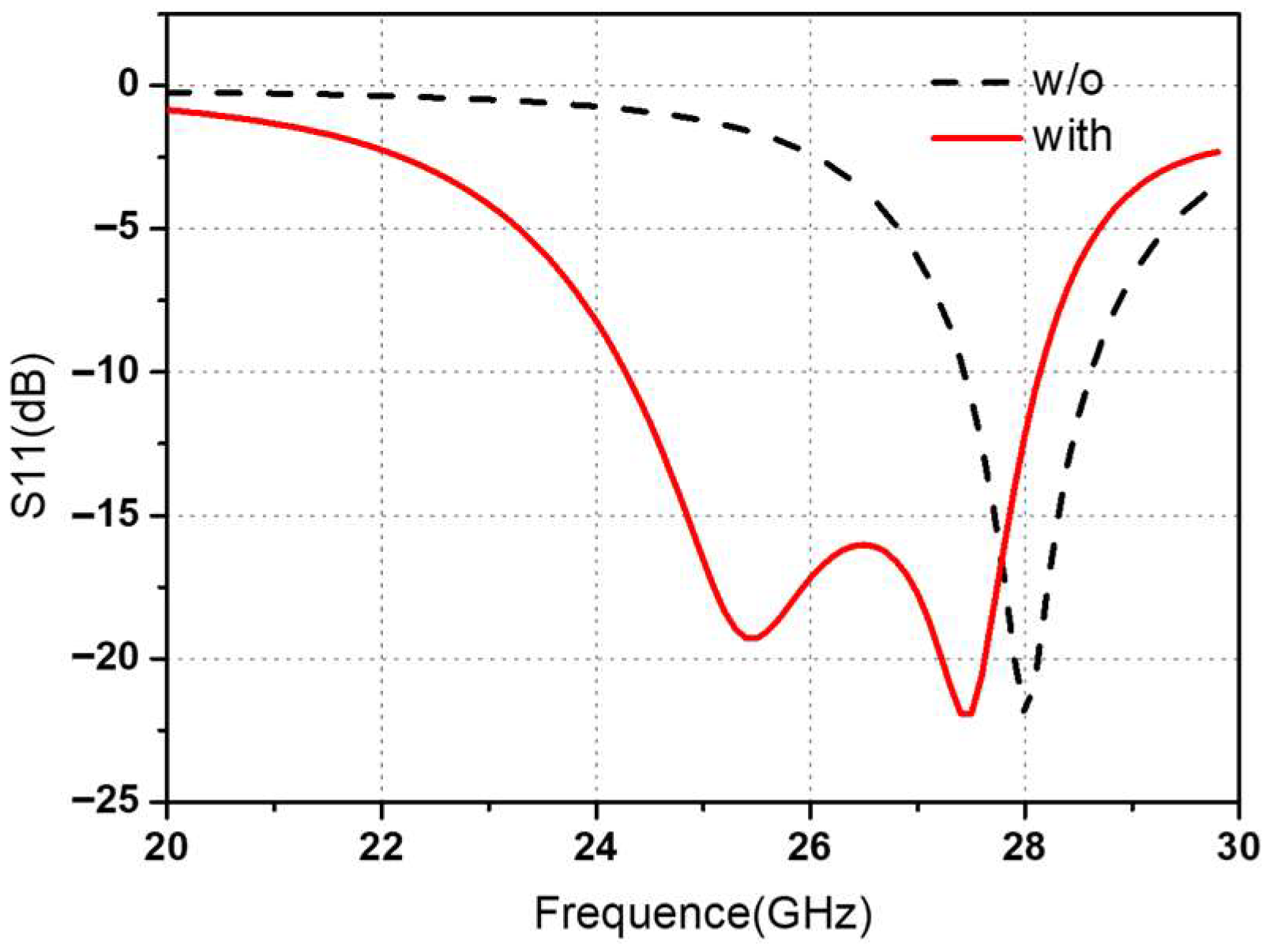
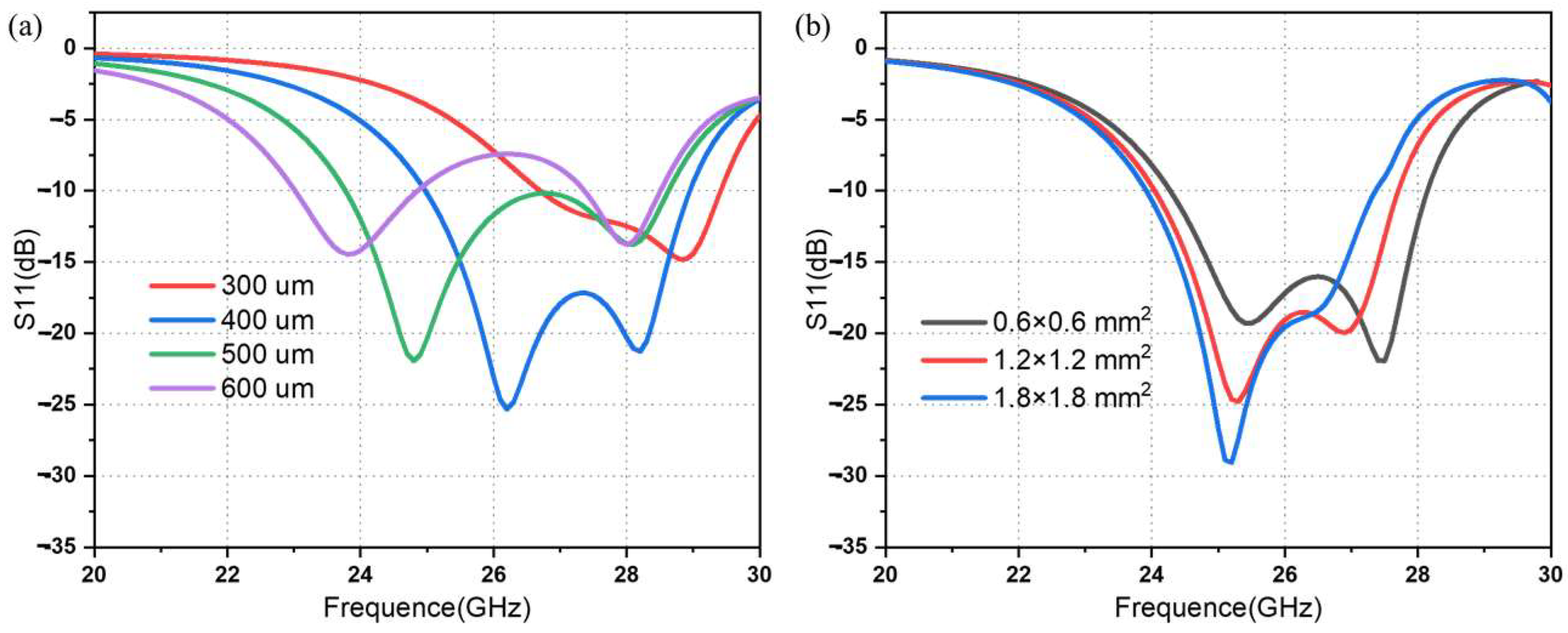
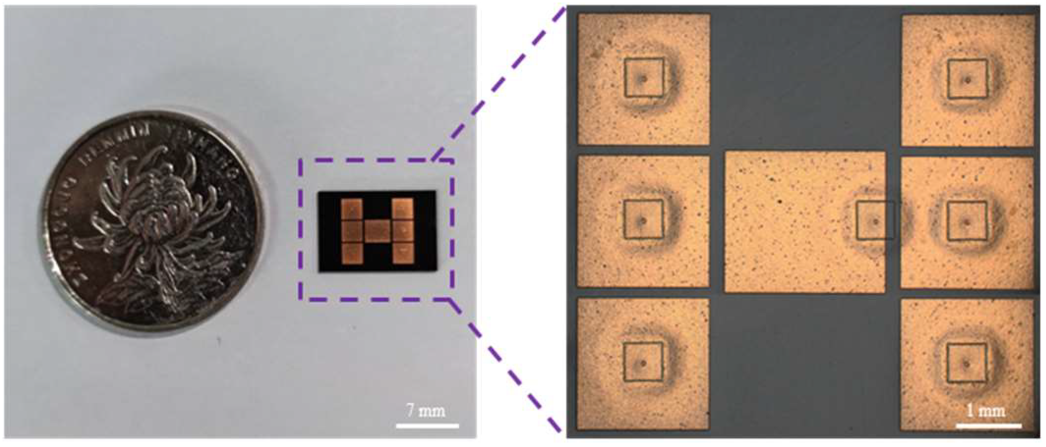
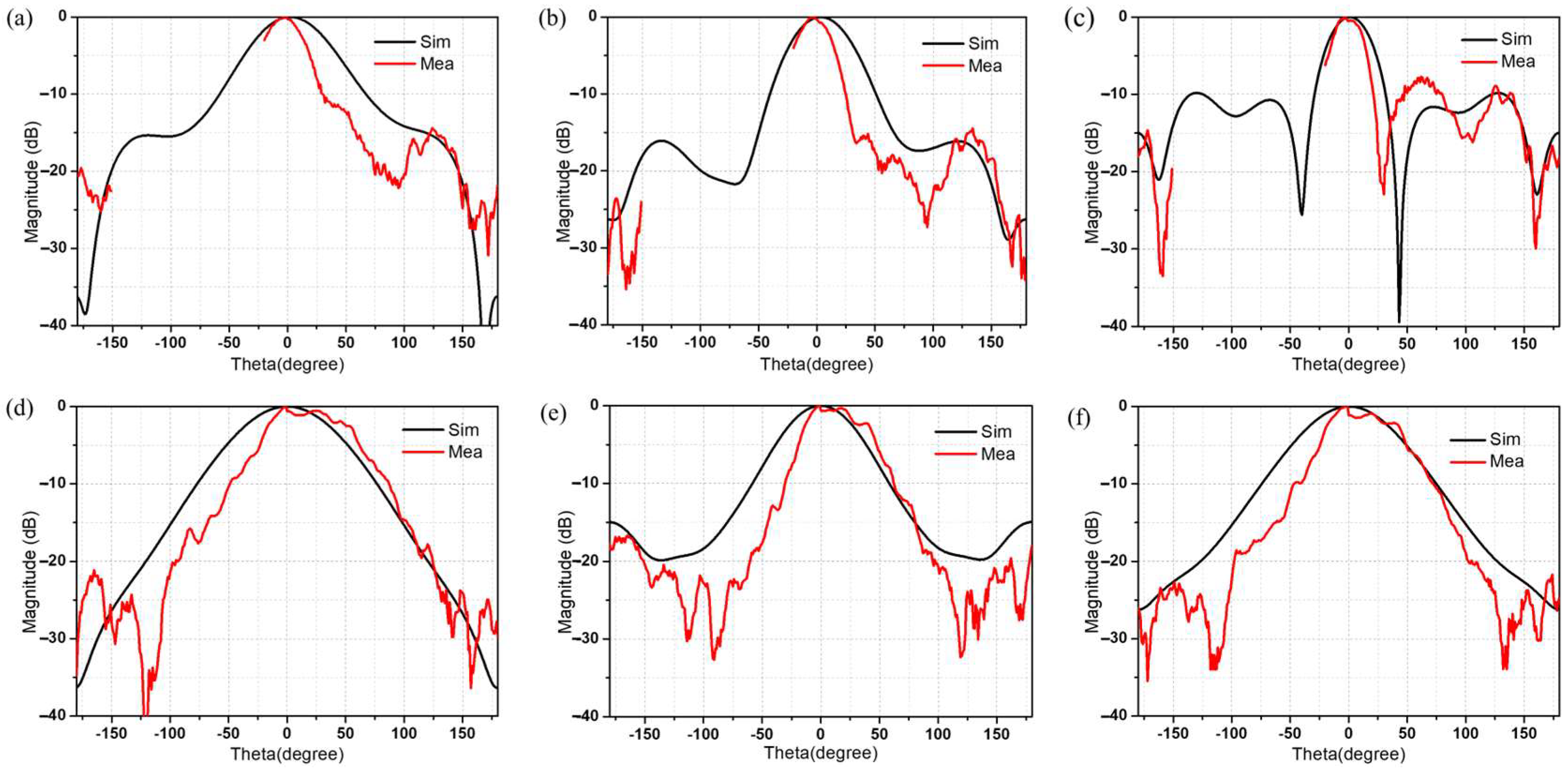
4. Antenna Performance

The parameters of the designed patch antenna were optimized using Ansys HFSS 2020R1 software and are listed in Table 1. The EMC used in the substrate has a relative permittivity of 3.93 and a loss tangent of 0.006. The dielectric polymer has a dielectric constant of 3.3 and a loss tangent of 0.008, and the coaxial feeding method was employed. The fabricated sample of the patch antenna element is shown in Figure 9.
A GSG probe was employed to establish contact with the feeding CPW line. The S-parameters of the fabricated samples were measured by utilizing a vector network analyzer. Additionally, the gains and radiation patterns of the samples were evaluated within an anechoic chamber, which provided accurate measurements of the antenna’s performance without interference from external reflections. The simulated and measured return losses and realized gains are shown in Figure 10. The measured results indicated that the −10 dB impedance bandwidth of the proposed patch antenna is 17% from 24.2 to 28.5 GHz, and the center frequency is 26.3 GHz. It was demonstrated that the patch antenna constructed via TMV-embedded FOWLP satisfied the frequency band used for 5G communications of n258 (24.25–27.5 GHz) and n261 (27.50–28.35 GHz). Moreover, as shown in Figure 10b, the measured gain was more than 7.5 dBi from 24.2 to 29.4 GHz. The gain at 26 GHz reached 9.1 dBi. Therefore, this patch antenna was capable of meeting the high gain and broadband requirements of 5G communications. The evaluated gains and radiation patterns, along with the expanded bandwidth achieved through the optimization techniques, make it well-suited for 5G communication applications, for which high performance and broad coverage are crucial.
The simulation and measurement results for the E- and H-plane radiation patterns of the proposed patch antenna are illustrated in Figure 11. The radiation patterns in the E-and H-planes presented good consistency at testing frequencies, and stable broadside radiation patterns for the patch antenna were realized. The measured results were slightly different from the simulated ones, which may be caused by process tolerance and a constant value of loss tangent in simulation at different frequencies.
In addition, comparisons with the previous related works are summarized in Table 2. All parameters were dependent on a single antenna element. Numerous works with PCB, LTCC, HDI, and FOWLP technologies operating at 5G frequency bands were embodied for comparison. The performance indicated that the proposed antenna possessed the advantages of a low profile, easy processing, and high gain.

5. Results

The designed patch antenna with a low profile and wide bandwidth was illustrated based on novel TMV-embedded FOWLP technology. The TMV-embedded package provided the possibility to realize low-loss interconnects. The element gain was higher than 7.5 dBi, and the return loss (|S11| ≤ 10 dB) ranged from 24.2 to 28.5 GHz, which covered the requirements of 5G systems. Therefore, the outstanding results of the designed patch antenna in this work demonstrated that the TMV-embedded FOWLP process is ideally suited for AiP for 5G mm-Wave application.

Author Contributions

Methodology, Y.Y. and C.X.; software, S.L.; investigation, Z.Z.; data curation, C.C.; writing—original draft preparation, Y.Y.; writing—review and editing, G.W. and Y.W.; supervision, G.W. and C.W. All authors have read and agreed to the published version of the manuscript.

Funding

This research received no external funding.

Data Availability Statement

Data is contained within the article.

Conflicts of Interest

Yuhang Yin, Chenhui Xia, Shuli Liu, Zhimo Zhang, Gang Wang, and Chenqian Wang was employed by the company The 58th Research Institute of China Electronics Technology Group Corporation. Yafei Wu, and Chen Chen declare that the research was conducted in the absence of any commercial or financial relationships that could be construed as a potential conflict of interest.

References

  1. Chowdhury, M.Z.; Shahjalal, M.; Ahmed, S.; Jang, Y.M. 6G wireless communication systems: Applications, requirements, technologies, challenges, and research directions. IEEE Open J. Commun. Soc. 2020, 1, 957–975. [Google Scholar] [CrossRef]
  2. Boric-Lubecke, O.; Lubecke, V.M.; Jokanovic, B.; Singh, A.; Shahhaidar, E.; Padasdao, B. Microwave and Wearable Technologies for 5G. In Proceedings of the 2015 12th International Conference on Telecommunication in Modern Satellite, Cable and Broadcasting Services (TELSIKS), Nis, Serbia, 14–17 October 2015; pp. 183–188. [Google Scholar]
  3. Huang, H.C.; Lu, J. Retrospect and Prospect on Integrations of Millimeter-Wave Antennas and Non-Millimeter-Wave Antennas to Mobile Phones. IEEE Access 2022, 10, 48904–48912. [Google Scholar] [CrossRef]
  4. Lin, T.H.; Kanno, K.; Watanabe, A.O.; Raj, P.M.; Tummala, R.R.; Swaminathan, M.; Tentzeris, M.M. Broadband and miniaturized antenna-in-package (AiP) design for 5G applications. IEEE Antennas Wirel. Propag. Lett. 2020, 19, 1963–1967. [Google Scholar] [CrossRef]
  5. Cheema, H.M.; Shamim, A. The last barrier: On-chip antennas. IEEE Microw. Mag. 2013, 14, 79–91. [Google Scholar] [CrossRef]
  6. Watanabe, A.O.; Ali, M.; Tehrani, B.; Hester, J.; Matsuura, H.; Ogawa, T.; Raj, P.M.; Sundaram, V.; Tentzeris, M.M.; Tummala, R.R. First Demonstration of 28 GHz and 39 GHz Transmission Lines and Antennas on Glass Substrates for 5G Modules. In Proceedings of the 2017 IEEE 67th Electronic Components and Technology Conference (ECTC), Orlando, FL, USA, 30 May–2 June 2017; pp. 236–241. [Google Scholar]
  7. Enayati, A.; Vandenbosch, G.A.E.; De Raedt, W. Millimeter-wave horn-type antenna-in-package solution fabricated in a teflon-based multilayer PCB technology. IEEE Trans. Antennas Propag. 2013, 61, 1581–1590. [Google Scholar] [CrossRef]
  8. Wu, Y.F.; Cheng, Y.J.; Huang, Z.X. Ka-band near-field-focused 2-D steering antenna array with a focused Rotman lens. IEEE Trans. Antennas Propag. 2018, 66, 5204–5213. [Google Scholar] [CrossRef]
  9. Wu, Y.F.; You, Q.; Zhang, Y.; Guo, Y.; Cheng, Y.J. Sidelobe Level Reduction for a W-Band SIW Slot Array Antenna by Only Reversing Offset Direction of Partial Slots. IEEE Trans. Antennas Propag. 2023, 71, 8360–8365. [Google Scholar] [CrossRef]
  10. Li, Y.; Wang, C.; Guo, Y.X. A Ka-band wideband dual-polarized magnetoelectric dipole antenna array on LTCC. IEEE Trans. Antennas Propag. 2019, 68, 4985–4990. [Google Scholar] [CrossRef]
  11. Kam, D.G.; Liu, D.; Natarajan, A.; Reynolds, S.; Chen, H.C.; Floyd, B.A. LTCC packages with embedded phased-array antennas for 60 GHz communications. IEEE Microw. Wirel. Compon. Lett. 2011, 21, 142–144. [Google Scholar] [CrossRef]
  12. Gu, X.; Liu, D.; Baks, C.; Tageman, O.; Sadhu, B.; Hallin, J.; Rexberg, L.; Valdes-Garcia, A. A Multilayer Organic Package with 64 Dual-Polarized Antennas for 28GHz 5G Communication. In Proceedings of the 2017 IEEE MTT-S International Microwave Symposium (IMS), Honololu, HI, USA, 4–9 June 2017; pp. 1899–1901. [Google Scholar]
  13. Xia, H.; Zhang, T.; Li, L.; Zheng, F.C. A Low-Cost Dual-Polarized 28 GHz Phased Array Antenna for 5G Communications. In Proceedings of the 2018 International Workshop on Antenna Technology (iWAT), Nanjing, China, 5–7 March 2018; pp. 1–4. [Google Scholar]
  14. Wang, C.T.; Tang, T.C.; Lin, C.W.; Hsu, C.W.; Hsieh, J.S.; Tsai, C.H.; Wu, K.C.; Pu, H.P.; Yu, D. InFO_AiP Technology for High Performance and Compact 5G Millimeter Wave System Integration. In Proceedings of the 2018 IEEE 68th Electronic Components and Technology Conference (ECTC), San Diego, CA, USA, 29 May–1 June 2018; pp. 202–207. [Google Scholar]
  15. Hsu, C.W.; Tsai, C.H.; Hsieh, J.S.; Yee, K.C.; Wang, C.T.; Yu, D. High Performance Chip-Partitioned Millimeter Wave Passive Devices on Smooth and Fine Pitch InFO RDL. In Proceedings of the 2017 IEEE 67th Electronic Components and Technology Conference (ECTC), Orlando, FL, USA, 30 May–2 June 2017; pp. 254–259. [Google Scholar]
  16. Tsai, C.H.; Hsieh, J.S.; Liu, M.; Yeh, E.H.; Chen, H.H.; Hsiao, C.W.; Chen, C.S.; Liu, C.S.; Lii, M.J.; Wang, C.T.; et al. Array Antenna Integrated Fan-Out Wafer Level Packaging (InFO-WLP) for Millimeter Wave System Applications. In Proceedings of the 2013 IEEE International Electron Devices Meeting, Washington, DC, USA, 9–11 December 2013; pp. 25.1.1–25.1.4. [Google Scholar]
  17. Rashidian, A.; Jafarlou, S.; Tomkins, A.; Law, K.; Tazlauanu, M.; Hayashi, K. Compact 60 GHz phased-array antennas with enhanced radiation properties in flip-chip BGA packages. IEEE Trans. Antennas Propag. 2018, 67, 1605–1619. [Google Scholar] [CrossRef]
  18. Zhang, Y.P.; Sun, M.; Lin, W. Novel antenna-in-package design in LTCC for single-chip RF transceivers. IEEE Trans. Antennas Propag. 2008, 56, 2079–2088. [Google Scholar] [CrossRef]
  19. Watanabe, A.O.; Lin, T.H.; Ali, M.; Wang, Y.; Smet, V.; Raj, P.M.; Tentzeris, M.M.; Tummala, R.R.; Swaminathan, M. Ultrathin antenna-integrated glass-based millimeter-wave package with through-glass vias. IEEE Trans. Microw. Theory Tech. 2020, 68, 5082–5092. [Google Scholar] [CrossRef]
  20. Zhang, Y.; Mao, J. An overview of the development of antenna-in-package technology for highly integrated wireless devices. Proc. IEEE 2019, 107, 2265–2280. [Google Scholar] [CrossRef]
  21. Rao, V.S.; Chong, C.T.; Ho, D.; Zhi, D.M.; Choong, C.S.; Sharon, L.P.; Liang, Y.Y. Development of high density fan out wafer level package (HD FOWLP) with multi-layer fine pitch RDL for mobile applications. In Proceedings of the 2016 IEEE 66th Electronic Components and Technology Conference (ECTC), Las Vegas, NV, USA, 31 May–3 June 2016; pp. 1522–1529. [Google Scholar]
  22. Hsieh, S.C.; Chu, F.C.; Ho, C.Y.; Wang, C.C. mmWave Antenna Design in Advanced Fan-Out Technology for 5G Application. In Proceedings of the 2019 22nd European Microelectronics and Packaging Conference & Exhibition (EMPC), Pisa, Italy, 16–19 September 2019; pp. 1–4. [Google Scholar]
  23. Le, T.H.; Kanitkar, A.; Rossi, M.; Ndip, I.; Braun, T.; Mueller, F.; Lang, K.D.; Wieland, M.; Goetze, C.; Halim, S.B.; et al. Dual-Band 5G Antenna Array in Fan-Out Wafer-Level Packaging (FOWLP) Technology. In Proceedings of the 2020 23rd International Microwave and Radar Conference (MIKON), Warsaw, Poland, 5–8 October 2020; pp. 157–161. [Google Scholar]
  24. Van Huylenbroeck, S.; Stucchi, M.; Li, Y.; Slabbekoorn, J.; Tutunjyan, N.; Sardo, S.; Iourdan, N.; Bogaerts, L.; Beirnaert, F.; Beyer, G.; et al. Small Pitch, High Aspect Ratio Via-Last TSV Module. In Proceedings of the 2016 IEEE 66th Electronic Components and Technology Conference (ECTC), Las Vegas, NV, USA, 31 May–3 June 2016; pp. 43–49. [Google Scholar]
  25. Töpper, M.; Ndip, I.; Erxleben, R.; Brusberg, L.; Nissen, N.; Schröder, H.; Yamamoto, H.; Todt, G.; Reichl, H. 3-D Thin Film Interposer Based on TGV (Through Glass Vias): An Alternative to Si-interposer. In Proceedings of the 2010 Proceedings 60th Electronic Components and Technology Conference (ECTC), Las Vegas, NV, USA, 1–4 June 2010; pp. 66–73. [Google Scholar]
  26. Kim, J.; Lee, K.; Park, D.; Hwang, T.; Kim, K.; Kang, D.; Kim, J.; Lee, C.; Scanlan, C.; Berry, C. Application of through Mold via (TMV) as PoP Base Package. In Proceedings of the 2008 58th Electronic Components and Technology Conference, Lake Buena Vista, FL, USA, 27–30 May 2008; pp. 1089–1092. [Google Scholar]
  27. Yu, B.; Qian, Z.; Lin, C.; Lin, J.; Zhang, Y.; Yang, G.; Luo, Y. A Wideband mmWave Antenna in Fan-Out Wafer Level Packaging with Tall Vertical Interconnects for 5G Wireless Communication. IEEE Trans. Antennas Propag. 2021, 69, 6906–6911. [Google Scholar] [CrossRef]
  28. Shibata, T.; Yoneda, S.; Li, X.; Suzuki, N.; Nonaka, T. Imprint-Through Mold via (i-TMV) with Highly-Effective Electromagnetic Interference Shielding for RF Devices. In Proceedings of the 2020 IEEE 8th Electronics System-Integration Technology Conference (ESTC), Tønsberg, Norway, 15–18 September 2020; pp. 1–4. [Google Scholar]
  29. Ho, S.W.; Boon, S.S.; Long, L.B.; Hsiang-Yao, H.; Choong, C.S.; Siang, S.L.P.; Chong, C.T. Double Mold Antenna in Package for 77 GHz Automotive Radar. In Proceedings of the 2020 IEEE 22nd Electronics Packaging Technology Conference (EPTC), Singapore, 2–4 December 2020; pp. 257–261. [Google Scholar]
  30. Long, L.B.; Ho, D.; Guan, L.T.; Yao, H.H.; Siang, L.P.; Jaafar, N. Fabrication Process Flow of Antenna-in-Package Fan-out Wafer Level Packaging. In Proceedings of the 2021 IEEE 23rd Electronics Packaging Technology Conference (EPTC), Singapore, 7–9 December 2021; pp. 226–230. [Google Scholar]
  31. Cao, Y.; Zhang, Y.; Cai, Y.; Zhang, J.; Qian, Z. Wideband and High Gain Patch Antenna Loaded with Mushroom-Type Metamaterial. In Proceedings of the 2018 International Conference on Microwave and Millimeter Wave Technology (ICMMT), Chengdu, China, 7–11 May 2018. [Google Scholar]
  32. Cao, Y.; Cai, Y.; Cao, W.; Xi, B.; Qian, Z.; Wu, T.; Zhu, L. Broadband and high-gain microstrip patch antenna loaded with parasitic mushroom-type structure. IEEE Antennas Wirel. Propag. Lett. 2019, 18, 1405–1409. [Google Scholar] [CrossRef]
  33. Du, J.K.; So, K.; Ra, Y.; Jung, S.Y.; Kim, J.; Kim, S.Y.; Woo, S.; Kim, H.T.; Ho, Y.C.; Paik, W. Dual-Polarized Patch Array Antenna Package for 5G Communication Systems. In Proceedings of the 2017 11th European Conference on Antennas and Propagation (EUCAP), Paris, France, 19–24 March 2017; pp. 3493–3496. [Google Scholar]
  34. Luo, Y.; Xu, J.; Chen, Y.; Sun, Y.; Xu, B.; Xu, S.; Yang, G. A Zero-Mode Induced mmWave Patch Antenna with low-Profile, Wide-Bandwidth and Large-angle Scanning for 5G Mobile Terminals. IEEE Access 2019, 7, 177607–177615. [Google Scholar] [CrossRef]
  35. Guo, G.; Wu, L.S.; Zhang, Y.P.; Mao, J.F. Stacked Patch Array in LTCC for 28 GHz Antenna-in-Package Applications. In Proceedings of the 2017 IEEE Electrical Design of Advanced Packaging and Systems Symposium (EDAPS), Haining, China, 14–16 December 2017; pp. 1–3. [Google Scholar]
  36. Hwang, I.J.; Jo, H.W.; Kim, J.W.; Kim, G.; Yu, J.W.; Lee, W.W. Vertically Stacked Folded Dipole Antenna Using Multi-Layer for mm-Wave Mobile Terminals. In Proceedings of the 2017 IEEE International Symposium on Antennas and Propagation & USNC/URSI National Radio Science Meeting, San Diego, CA, USA, 9–14 July 2017; pp. 2579–2580. [Google Scholar]
  37. Ahn, K.; Park, J.; Lee, B.; Kang, L.; Kim, J.; Shin, K.; Kim, S.H.; Lee, J.D.; Kim, M.K.; Lee, H.S. Chip-Last FOWLP Based Antenna-in-Package (FO-AiP) for 5G mmWave Application. In Proceedings of the 2022 IEEE 72nd Electronic Components and Technology Conference (ECTC), San Diego, CA, USA, 31 May–3 June 2022; pp. 1384–1389. [Google Scholar]
Figure 1. Illustration of a TMV-embedded FOWLP.
Electronics 13 00839 g001
Figure 2. Process flow of the TMV-embedded FOWLP technology.
Electronics 13 00839 g002
Figure 3. Optical images of (a) TMV interposer embedded in reconstituted wafer, (b) the front side RDL, (c) reconfigured wafer back side after thinning, and (d) cross-section SEM image of the package.
Electronics 13 00839 g003
Figure 4. Topology of the coplanar waveguide (CPW) structure. The black is substrate and the yellow is metal.
Electronics 13 00839 g004
Figure 5. (a) Stack-up, (b) 3D, and (c) top views of the patch antenna.
Electronics 13 00839 g005
Figure 6. Simulated |S11|of the patch antenna with and without the symmetrical parasitic patch.
Electronics 13 00839 g006
Figure 7. Variation trend of |S11|s in relation to (a) TMV height and (b) TMV size.
Electronics 13 00839 g007
Figure 8. Variation trend of |S11| in relation to different (a) a and (b)c values.
Electronics 13 00839 g008
Figure 9. Optical micrographs of the proposed patch antenna.
Electronics 13 00839 g009
Figure 10. Simulated and measured (a) S11 and (b) gain of the proposed miniaturized patch antenna element.
Electronics 13 00839 g010
Figure 11. Simulated and measured far-field radiation patterns for proposed patch antenna: (a) 24 GHz E-plane, (b) 26 GHz E-plane, (c) 28 GHz E-plane, (d) 24 GHz H-plane, (e) 26 GHz H-plane, and (f) 28 GHz H-plane.
Electronics 13 00839 g011
Table 1. The optimized parameters of the antenna element.
ParameterValue (mm)ParameterValue (mm)
L12.841c0.272
W12.519h0.45
L21.255d0.1
a2.333W9.018
b0.185L13.128
Table 2. Comparison with the previous related works.
WorkTechniqueFrequency (GHz)Number of LayerThickness (λ0)FWB (%)Gain (dBi)Antenna
Type
[33]HDI27.5–29.580.0727.01%4.0Patch
[34]PCB23.5–2830.04417.4%6.0Patch
[27]FOWLP25–4320.11964.3%5.0ME dipole
[35]LTCC26.3–29.8100.09012.4%3.1Patch
[36]PCB27.5–29.5100.0769.3%5.7Yagi-Uda
[37]FOWLP26.5–29.720.04212.1%5.3Patch
This workTMV-embedded FOWLP24.2–28.510.04017.8%7.5Patch
Disclaimer/Publisher’s Note: The statements, opinions and data contained in all publications are solely those of the individual author(s) and contributor(s) and not of MDPI and/or the editor(s). MDPI and/or the editor(s) disclaim responsibility for any injury to people or property resulting from any ideas, methods, instructions or products referred to in the content.

