Article

A Fast Repetitive Control Strategy for a Power Conversion System

1
School of Electrical and Control Engineering, North China University of Technology, 5 Jinyuanzhuang Road, Shijingshan District, Beijing 100043, China
2
Beijing Laboratory of New Energy Storage Technology, Beijing Municipal Education Commission, Beijing 100083, China
3
Shanghai Electrical Apparatus Research Institute, Building 1, No. 505 Wuning Road, Putuo District, Shanghai 200333, China
*
Author to whom correspondence should be addressed.
Electronics 2024, 13(7), 1186; https://doi.org/10.3390/electronics13071186
Submission received: 11 February 2024 / Revised: 11 March 2024 / Accepted: 19 March 2024 / Published: 23 March 2024

Abstract

:
With the expansion of renewable energy sources, the stable and high-quality operation of microgrids composed of new energy sources has attracted widespread attention. Among them, the power conversion system (PCS), as an important part of microgrids, plays a crucial role in their operation and management. The PCS operation modes are classified into grid-connected and off-grid modes. However, in off-grid mode, due to the access of nonlinear and unbalanced loads, the output voltage quality of a PCS is worse, and the voltage waveform distortion is serious. To solve these problems, a fast repetitive control (FRC) strategy is proposed for a power conversion system with an Active Neutral Point Clamped (ANPC) architecture of three levels. The voltage loop control strategy can be applied to the voltage/frequency ( V / f ) mode and the grid-forming mode. The control strategy can effectively realize the suppression of the harmonics of the output voltage and has a 100% capability to carry unbalanced loads. Finally, a 1725 kVA PCS prototype is developed, and the proposed control strategy is verified using the MT3200 HIL semiphysical simulator of ModelingTech in the V / f mode as an example. This practically verifies the feasibility and validity of the proposed control strategy, which has a certain degree of engineering practicability and reference due to the simplicity of the design and the ease of realization.

1. Introduction

In order to foster an eco-friendly society and ensure sustained and stable growth of the national economy, China has embarked on a robust initiative to promote clean energy. This initiative serves as a key measure to bolster the nation’s energy competitiveness and addresses the pressing imperatives of climate change mitigation, ecological preservation, and the attainment of sustainable economic and social development in China. Concurrently, as part of the overarching blueprint for ecological civilization construction, China has set forth the ambitious “2030 carbon peak” and “2060 carbon neutral” dual carbon objectives [1]. This strategic framework aims to cultivate a novel power system wherein new energy sources take precedence [2].
A microgrid, comprised of PCS energy storage inverters, is capable of grid-connected operation with the main power grid and off-grid operation to independently supply power to loads. Due to its distinct characteristics of generation (“source”), consumption (“load”), and storage (“storage”), the microgrid stands as a vital component of a novel power system dominated by renewable energy sources [3].
In the off-grid operation mode of PCS, there are primarily two control modes: (1) Constant Voltage–Frequency ( V / f ) Control and (2) Grid-Forming (GFM) Control. Both droop control [4] and virtual synchronous machine control [5,6] fall under the category of GFM control [7]. Regardless of whether it is V / f control or GFM control, voltage regulation is essential to control the output voltage of a PCS. Different voltage control strategies play a crucial role in determining the quality of the PCS output voltage.
Currently, common voltage control strategies applicable to PCS include the following:
  • Proportional–Integral (PI) Control: Using dq coordinate systems, PI control achieves voltage regulation but lacks harmonic suppression and the capability of operating with unbalanced loads. If it is necessary to add harmonic suppression, and in order to cope with three-phase unbalanced loads on top of PI control, an additional VPI controller is required [8,9]. This approach requires the design of additional parameters, greatly increasing the design complexity, which is not conducive to engineering implementation.
  • Proportional Resonant (PR)/Quasi-Proportional Resonant (QPR) Control [10]: Based on internal model principles and utilizing abc or α β coordinate systems, PR/QPR control regulates output voltage without harmonic suppression. Its ability to independently control three-phase voltages allows operation with unbalanced loads.
  • Proportional Multiresonant Control (PMR) [11]: As an enhanced version of PR control, PMR control consists of multiple PR controllers in parallel, providing both harmonic suppression and the capability of operating with unbalanced loads. However, its structure is complex, requiring the tuning of multiple control parameters.
  • Repetitive control (RC) [12]: Also based on internal model principles, RC control is simple in structure and capable of harmonic suppression and operation with unbalanced loads. However, its dynamic performance may be less favorable. To address the dynamic performance issues of repetitive control, some scholars have proposed odd repetitive control [13], which speeds up the dynamic performance but lacks the suppression of even harmonics.
  • Model Predictive Control (MPC) [14,15]: Carrier-based modulated MPC strategies have demonstrated potential for harmonic suppression and operation with unbalanced loads. However, effective MPC controller design requires careful consideration of dynamic system characteristics, constraints, performance metrics, and computational complexity.
  • Robust Control [16,17]: Exhibiting strong robustness, robust control requires a good understanding of system uncertainties and the careful selection of weighting functions. Experimental and simulation methods may be necessary to validate and adjust robust control strategies for reliable application.
  • Sliding Mode Control (SMC) [18,19]: Leveraging strong robustness and nonlinear characteristics, the SMC exhibits capabilities for harmonic suppression and operation with unbalanced loads. However, in practical applications, precise modeling of system dynamics and careful adjustment of controller parameters are essential. Additionally, SMC may introduce high-frequency oscillations, necessitating appropriate design and tuning to balance system performance and stability.
This paper focuses on the ANPC three-level energy storage inverter and proposes a rapid repetitive control strategy. The study adopts a composite control structure that combines proportional control with repetitive control. The proposed control strategy is characterized by its simplicity in design and ease of engineering implementation. Experimental validation on a 1725 kVA power conversion system confirms that the proposed control strategy can achieve optimized output voltage waveforms under both V/f control and grid-forming control.

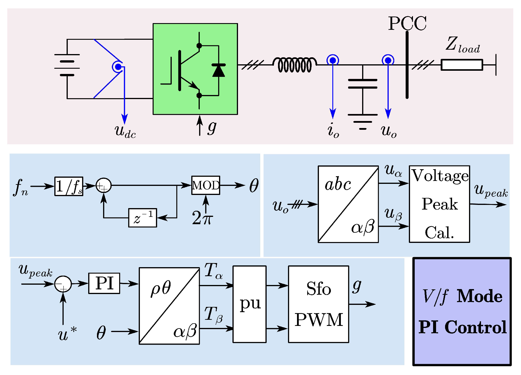
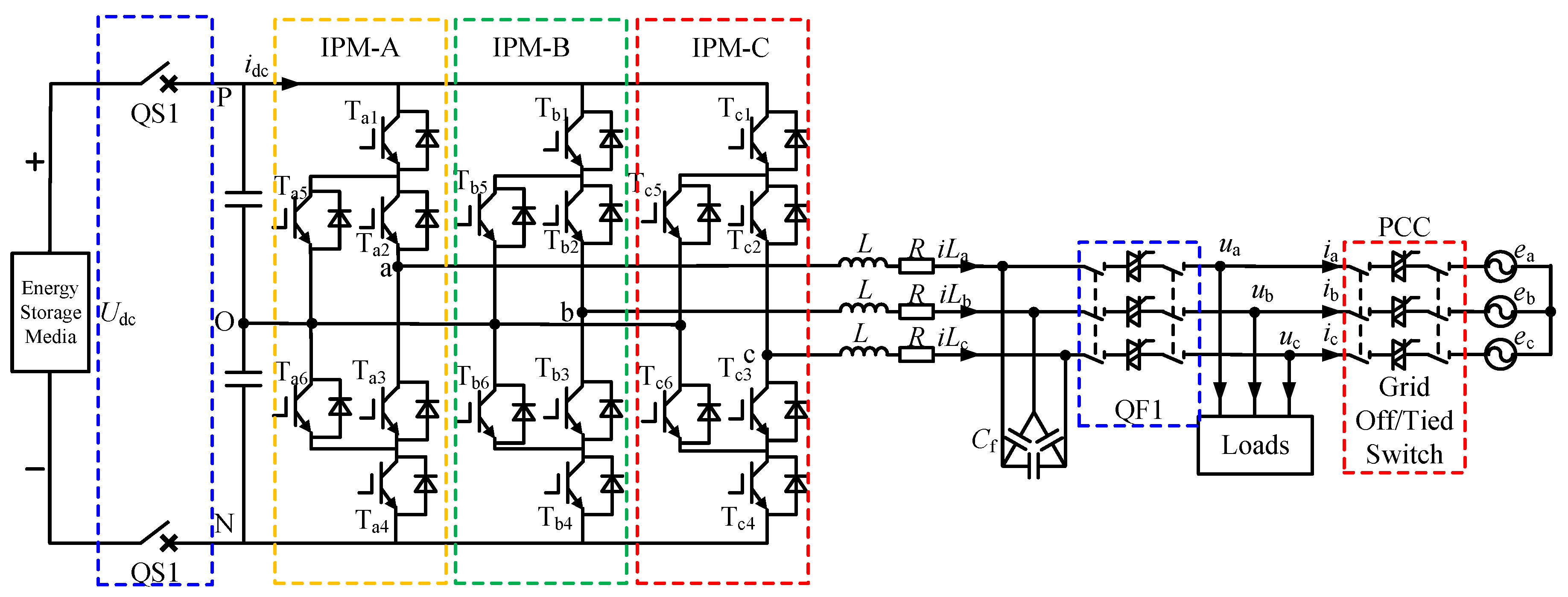
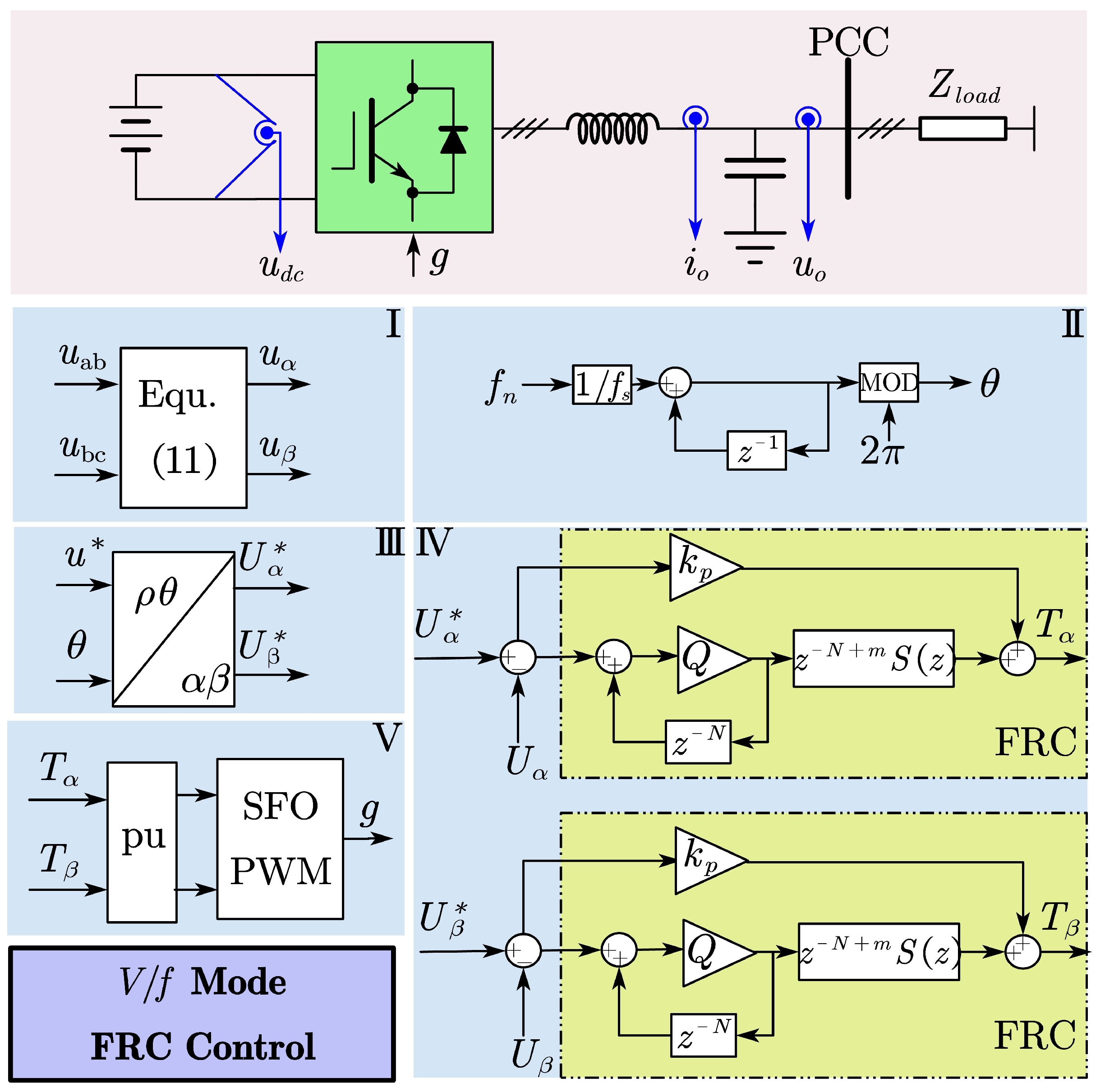
2. ANPC Three-Level PCS Modeling

With a two-level topology, each IGBT/MOSFET is required to withstand the entire DC bus voltage stress. This leads to the process of selecting the half-bridge module, which must have a module that withstands a voltage value of U d c above the voltage level (at least 1.2 times). As a result, the DC side voltage of the two-level is generally lower than 1000 V. Furthermore, in the chain reaction brought about by voltage stress, the d v / d t becomes larger, causing a serious problem. The large d v / d t introduces serious electromagnetic interference (EMI) problems, which make hardware design difficult, with large switching losses leading to low efficiency.
Compared to the two-level structure, the three-level structure offers several advantages [20]:
  • Enhanced power quality and increased power density: With higher output levels, the output voltage waveform is closer to sinusoidal, improving the power quality of the output waveform. This design also reduces the size of the filter and increases the power density of the system, especially under the same switching frequency [21].
  • Improved efficiency: The three-level structure primarily utilizes the Neutral Point Clamped (NPC) topology, which includes I-type NPC, T-type NPC, and ANPC (Active Neutral Point Clamped) [22].
In this paper, we will focus on ANPC [23]. The relevant parameters of the PCS system in this paper are shown in Table 1, with a rated capacity of 1725 kVA.
Figure 1 provides the basic topology of the 1725 kVA PCS based on an ANPC type three level. The QS1 is the internal DC circuit breaker of a PCS, and the IPM-A/B/C is the switching device (IGBT) composed of the ANPC topology. L represents the three-phase filter inductors, R is the phase-to-phase DC resistance of the filter inductors, and the filter capacitor C f takes a delta-type connection. The QF1 is the internal AC circuit breaker of the PCS. The grid switch is at the point of common coupling (PCC), which is the external switch of the PCS.
From Figure 1 and combined with Kirchhoff’s voltage law, the mathematical model of the three-level converter in the three-phase stationary coordinate system can be obtained as follows:
e x = L d i L x d t + R i x + u x i L x = C d u x d t + i x ,
where x = a , b , c , e x denotes the bridge arm voltage, and C is the filter capacitor (C = 3 C f ) after the angle-star connection equivalent. i L x indicates the bridge arm current flowing through phases A, B, and C. u x denotes the load terminal voltage, and i x is the PCS output current.
After modeling the three-level ANPC inverter, the design of the FRC is carried out. To simplify the design of the FRC, the Clarke transformation is conducted, moving from a three-phase stationary coordinate system to a two-phase static coordinate system as follows:
L d i L α d t = e α R i L α u α C d u α d t = i L α i α
L d i L β d t = e β R i L β u β C d u β d t = i L β i β .
From (2) and (3), there is no coupling on the axis. Further Laplace transform of (2) and (3) gives the relationship between the input and output of the system as
e α = 1 L C s 2 + R C s + 1 u α L s + R L C s 2 + R C s + 1 i α
e β = 1 L C s 2 + R C s + 1 u β L s + R L C s 2 + R C s + 1 i β .
The transfer function G ( s ) of the output voltage and input voltage of the PCS is obtained from (4) and (5):
G s = 1 L C s 2 + R C s + 1 .
The equivalent output impedance of the PCS is
Z 0 = L s + R L C s 2 + R C s + 1 .
In the 1725 kVA PCS, the LC forms a resonant network. If the system is unloaded, there will be a resonance peak. At this time, the system stability is the worst; so, the FRC should be designed assuming the no-load case. From (4) and (5), it can be seen that in the no-load case of the PCS, the transfer function of the controlled object P ( s ) is
P s = 1 L C s 2 + R C s + 1 .
The main circuit parameters of the 1725 kVA PCS are shown in Table 2.
From Table 2 and (8), the discrete time is taken as 1/3600 s, and the discrete transfer function of the controlled object is equal to
P z = 0.4511 z + 0.279 z 2 0.5192 z + 0.2494 .
The Bode diagram of P ( z ) is given in Figure 2. In the 1 kHz band, the LC resonates, and the phase frequency characteristic has a jump of −180° to 180° at this frequency. Due to the filter inductor L in the LC filter, there is a DC resistance; so, the resonance peak of the amplitude–frequency characteristics of P ( z ) is not apparent. Based on this 1725 kVA PCS, no damping strategy was incorporated. Therefore, in the subsequent design of the FRC, this resonance point should be avoided or attenuated as much as possible.

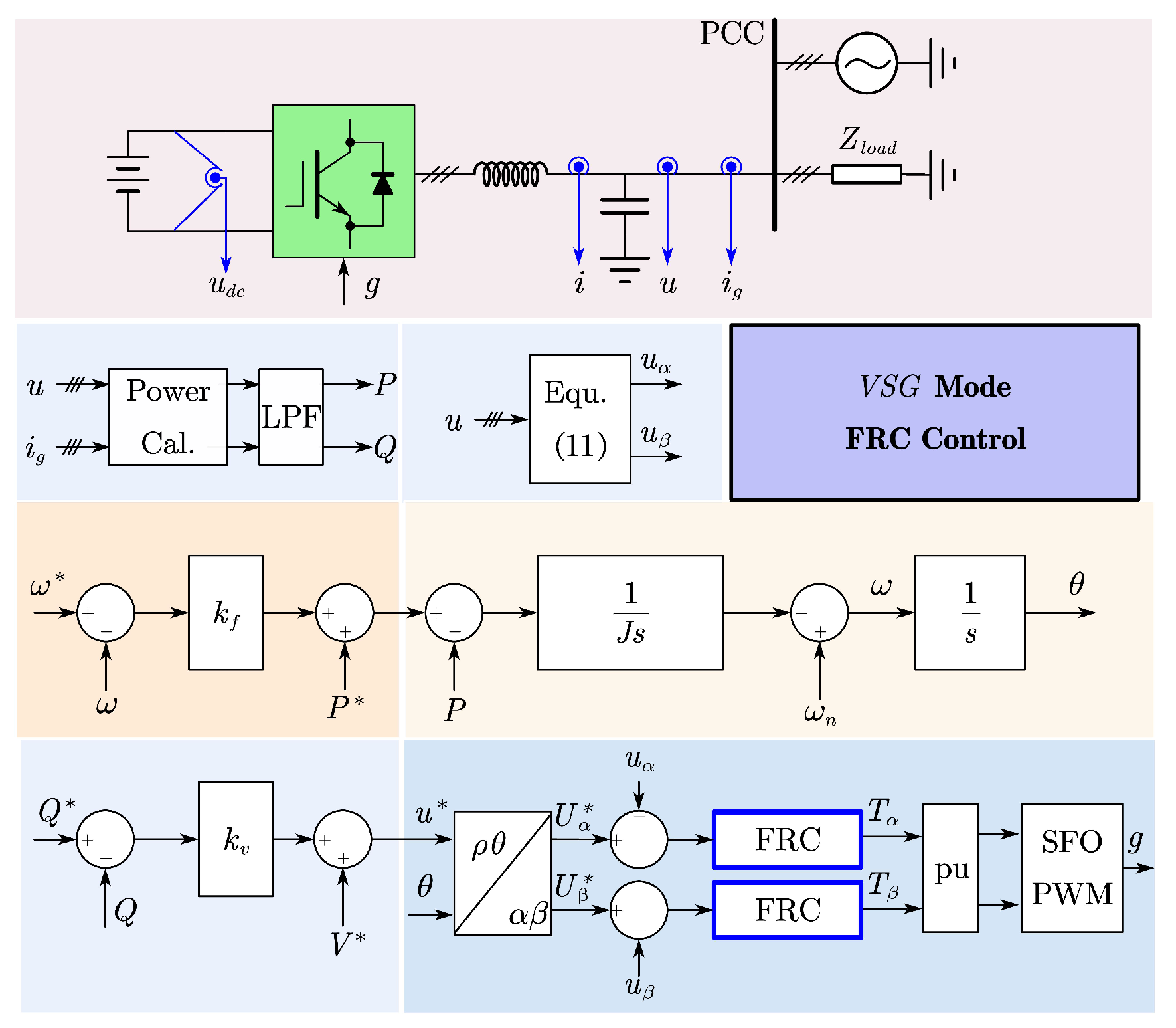
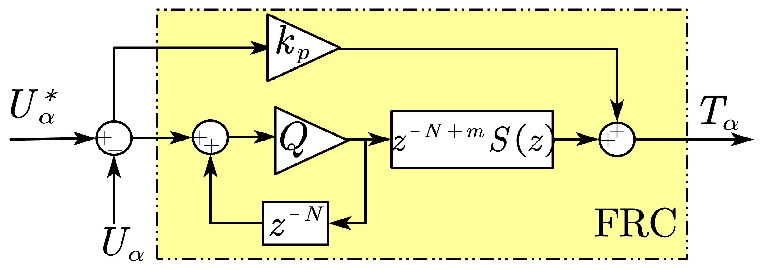
3. The Proposed Scheme

Proportional Integral (PI) control is less effective for an AC input signal; so, the conventional method is converted to the d q axis. However, this method does not have harmonic suppression capability and cannot deal with unbalanced loads. For this reason, an FRC scheme is proposed in this paper. The block diagram of the proposed FRC is shown in Figure 3.
In Figure 3, U α * is the reference voltage signal; U α is the instantaneous voltage value of the PCS output voltage after coordinate transformation to the axis α ; k p is the gain of the FRC; Q is the internal mode (can choose a constant slightly less than 1 or a zero-phase-shift low-pass filter); N is the modulation ratio ( f s / f n ), where f s is the switching frequency, and f n is the normal voltage frequency; m is the phase compensation coefficient and S ( z ) is the low-pass filter. The transfer function of the FRC can be obtained from Figure 3, as follows:
G FRC = Q z N + m S z 1 Q z N + k p .
The whole control block of the system for the 1725 kVA PCS in V / f mode is shown in Figure 4.
In Figure 4, u d c represents the system’s DC voltage, i 0 represents the system’s output current, and u o represents the system’s voltage. The blue lines represent sampling; the components are as follows:
I is the 3/2 transformation: The output voltages U a b and U b c are sampled from the system and transformed from a three-phase a b c stationary coordinate system to a two-phase static coordinate system with the following transformation (11). The specific derivation is given in Appendix A.1.
U α = u a b U β = 1 3 ( u a b + 2 u b c ) ;
II is the generation of the output voltage angle θ of PCS, f n is the rated frequency, f s is the sampling frequency;
III is the generation of the reference voltage amplitude, the output voltage amplitude can be set via u * ;
IV are the two FRC voltage controllers, output T a l p h a and T b e t a , respectively;
V is the generation of six drive signals per phase to the IPM A/B/C, shown in Figure 1, using SFO-PWM.

4. Parameter Design and Analysis of the Proposed FRC

From Figure 4, it can be seen that the design of an FRC is the same in the three-phase stationary coordinate system as in the two-phase static coordinate system. Here, the design of the α -axis is taken as an example, and the β -axis is the same.

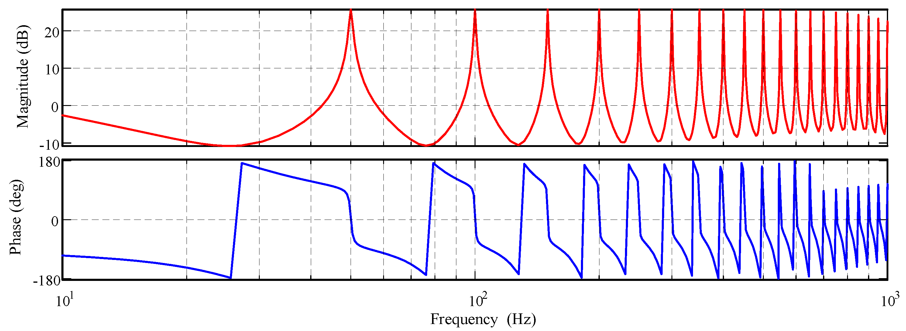
4.1. Stability Analysis

As shown in Figure 4, the error transfer function of the system is
E z = U α * U α 1 + G F R C z P z .
The polynomial of the error transfer function of the FRC control system is
1 + G F R C P z = 1 + Q z N + m S z 1 Q z N + k p P z .
To ensure stability, it should be guaranteed that the roots of the characteristic equations of the closed-loop system are inside the unit circle. Observing (13), the equation does not help design the parameters, due to the coupling. Let
G r c z = Q z N + m S z 1 Q z N .
Then, Equation (13) after decoupling becomes
1 + G r c z ) + k p ] · P z = [ 1 + k p P z · 1 + G r c z P z 1 + k p P z ] = [ 1 + k p P z · 1 + G r c z · P 0 z ] .
Among these,
P 0 z = P z 1 + k p P z .
The stability criterion of the FRC can be obtained from (15), as follows:
Condition 1: The roots of [ 1 + k p P z ] = 0 are inside the unit circle.
Condition 2: The roots of 1 + G r c z · P 0 z = 0 are inside the unit circle.
According to Condition 1, a suitable k p can be selected. From Condition 2, (14), and (16), we obtain
1 + Q z N + m S z 1 Q z N P 0 z < 0 .
Since 1 Q z N 0 , the left and right sides of (17) are simultaneously multiplied by 1 Q z N .
Q z N [ 1 z m S z P 0 z ] < 1
When the frequency is the fundamental wave or an integer multiple of the fundamental wave frequency, Q z N 1 .
1 z m S z P 0 z < 1
Denote the amplitude and phase characteristics of S ( z ) and P 0 ( z ) as
S ( j ω ) = N S ω e j θ S ω ,
P 0 ( j ω ) = N P 0 ω e j θ P 0 ω .
Substituting (20) and (21) into (19) yields
1 N S ω N P 0 ω e j θ s ω ) + θ P 0 ω ] + m ω < 1 .
According to Euler’s formula,
e j θ s ω ) + θ P 0 ω ] + m ω = cos { θ s ω ) + θ P 0 ω ] + m ω } j sin { θ s ω ) + θ P 0 ω ] + m ω } .
Let
φ = θ s ω + θ P 0 ω + m ω .
According to (22)–(24), we can obtain
( 1 N s ω N P 0 ω cos φ ) j N s ω N P 0 ω sin φ < 1 .
Taking the square of (25) gives
N s ω N P 0 ω ) ] 2 + 1 + 2 N s ω N P 0 ω cos φ < 1 .
Simplify (26) to obtain
N s ω N P 0 ω < 2 cos φ .
Since N s ω N P 0 ω > 0 , the final judgment is obtained as follows:
90 < φ < 90 .
This section started from the system error transfer function and ended with Condition 1 and Condition 2. Condition 1 provides a reference for the design of k p , and Condition 2 is simplified to obtain the creation of the FRC phase compensation coefficient m. In the following subsection, how to use these two Conditions for the design of the FRC parameters will be explained in detail.

4.2. Parameter Design of an FRC

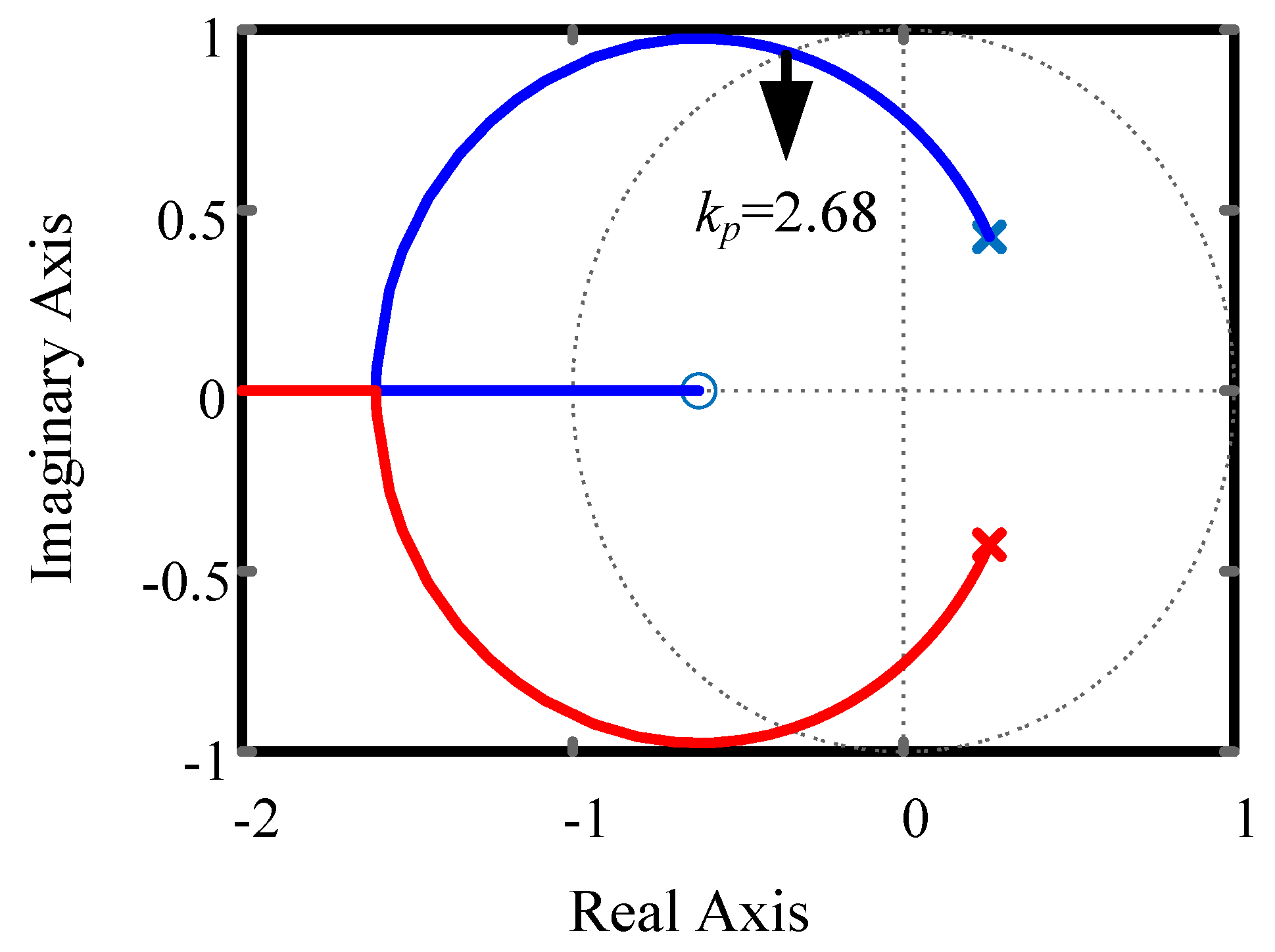
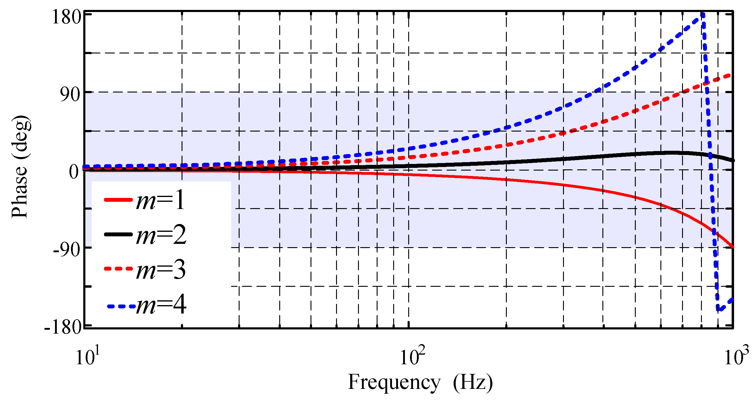
4.2.1. FRC Gain Coefficient k p

From Condition 1, the k p of the FRC can be designed. Due to the structural characteristics of the FRC itself, the output signal will lag behind the input signal by N beats, and the dynamic performance of the entire control system is poor at tracking the input signal quickly. Therefore, the proportional coefficient k p is connected in parallel. k p will provide a fast channel for the error, and the output of the proportional coefficient k p will directly change the size of the regulation system to realize the quick adjustment function.
A smaller k p will make the system’s dynamic performance worse, and a larger k p will make the system’s stability worse. Meanwhile, according to (16), there is a coupling relationship between k p and P 0 ( z ) . Different k p s will lead to different amplitude and phase frequency curves of P 0 ( z ) . In the design of phase compensation z m , the actual compensation object is P 0 ( z ) . Therefore, k p should not be too large, because it will fluctuate the phase of P 0 ( z ) . If the phase lag of P 0 ( z ) is too significant, the phase compensation coefficient m will be excessive, and according to (24) and (28), too large an m or too long a phase lag of P 0 ( z ) will cause the stability margin of the system to be small or unstable.
Based on Condition 1, a graph of the root trajectory of P ( z ) is given under different k p s. The maximum k p = 2.68 can be obtained according to Figure 5.
According to (15), the FRC controls P 0 ( z ) as a generalized controlled object, and the Bode diagram of P 0 ( z ) is given in Figure 6. With increasing k p , the phase change in P 0 ( z ) in the middle− and low−frequency bands becomes smaller; however, at the same time, the stability of P 0 ( z ) decreases. When k p exceeds 2, the system’s resonance has started to seriously affect the system’s stability.
With the comprehensive consideration of the above two factors, the FRC phase compensation z m and the dynamic performance of the system. k p is chosen as 0.2; at this time, the GM = 7.93 dB, and the PM = deg.

4.2.2. FRC Internal Model Coefficient Q

Q is a key parameter used by the FRC to enhance system stability and achieve the static-free tracking of a reference signal. Q is usually taken as a constant or a low-pass filter slightly less than 1. When Q is a constant, the closer it is to 1, the smaller the steady-state error of the system, and the stronger the harmonic suppression ability. In this work, we take Q as a zero-phase-shift low-pass filter which has no effect on low-frequency signals and quickly attenuates high-frequency signals to improve system stability. The expression of a zero-phase-shift low-pass filter is as follows:
Q z = i = 0 I α i z i + i = 1 I α i z i .
In (29), we have α 0 + 2 i = 1 m α i = 1 , α i > 0 , and the first-order zero-phase-shift low-pass filter can be expressed as
Q z = z + α 0 + z 1 2 + α 0 .
We can see from Figure 7 that with the small value of α 0 , Q attenuates the high-frequency signal more strongly; so, we choose α 0 equal to 2. When α 0 is equal to 2, Q has basically no effect on the base frequency signal (50 Hz), which means that we can realize the non-differential tracking, and for the high-frequency signal (greater than 1 kHz), Q has begun to attenuate the high-frequency signal, which is beneficial for the stability of the system.

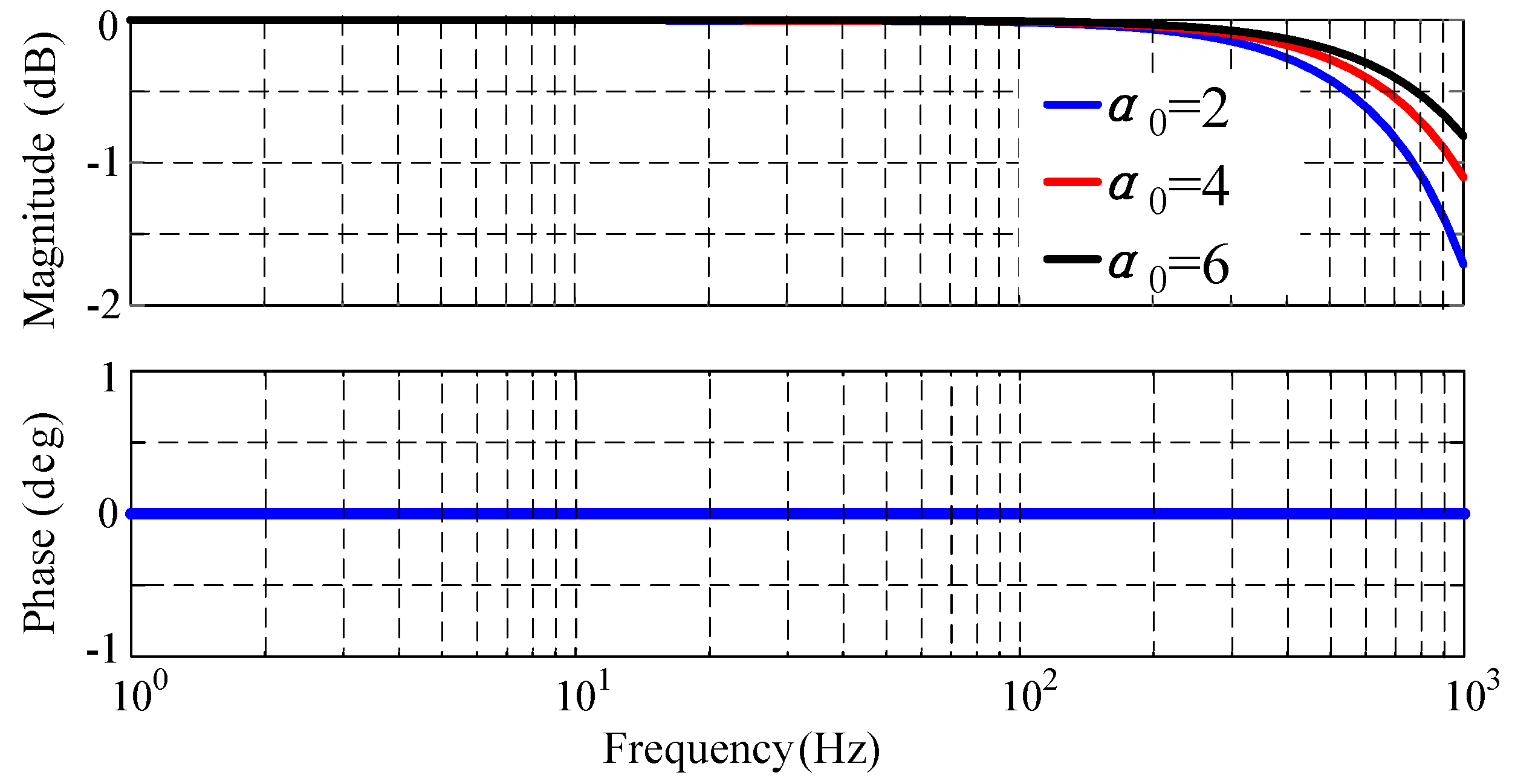
4.2.3. FRC Compensator S ( z )

Compensator S ( z ) mainly attenuates the gain brought about by the FRC in the high-frequency band, as well as the strong attenuation of high-frequency disturbing signals in the control system, due to the existence of the compensator S ( z ) , and the system stability performance can be significantly increased. The Butterworth low-pass filter is used in this work because it has zero phase shift in the low-frequency band. As the order of the Butterworth low-pass filter increases, the Butterworth low-pass filter attenuates the signals after the cutoff frequency more strongly, and the filtering effect will be better. However, at the same time, it will also bring about the problem of phase lag. In addition, in the digital control system, a too-high order level will cause a certain computational delay and increase the computational burden of the DSP.
The design of this filter is simple and can be obtained by writing a few lines of the m-language using MATLAB, which is given in Appendix E. The resonant frequency of the LC filter in Figure 2 is around 1 kHz; so, we set the cutoff frequency of the second-order Butterworth low-pass filter to be 1 kHz. The discrete time is 1/3600 s, and the transfer function is obtained as
S z = 0.3459 z 2 + 0.6919 z + 0.3459 z 2 + 0.2047 z + 0.179 .

4.2.4. FRC Phase Lead Compensation z m

z m is mainly used to compensate for the phase lag introduced by S ( z ) and P 0 ( z ) . A suitable z m should compensate for phase S ( z ) and P 0 ( z ) at about 0 deg. The phase frequency characteristic curves of S ( z ) and P 0 ( z ) with different ms are given in Figure 8.
From (28), the stable region in Figure 8 is the shaded part. When m = 1 , the system is under−compensated, and the phase lag of the system in the low−frequency and mid−frequency bands is quite severe. In the frequency band of 1 kHz, it is about to go beyond the shaded part, and the stability performance is weak. When m = 2 , the system can meet the stability conditions, while in the frequency band below 1 kHz, there is no significant phase lag. When m = 3 , the system is in overcompensation, and the phase angle of compensation has exceeded 90°, beyond the stability region. Similarly, when m = 4 , the steady state condition is not satisfied; so, m is chosen as 2.
The parameters of the FRC are obtained from the above analysis, as shown in Table 3.
According to Table 3, the open-loop Bode plot of the FRC in the discrete domain (with a discrete time of 1/3600 s) is obtained, as shown in Figure 9.

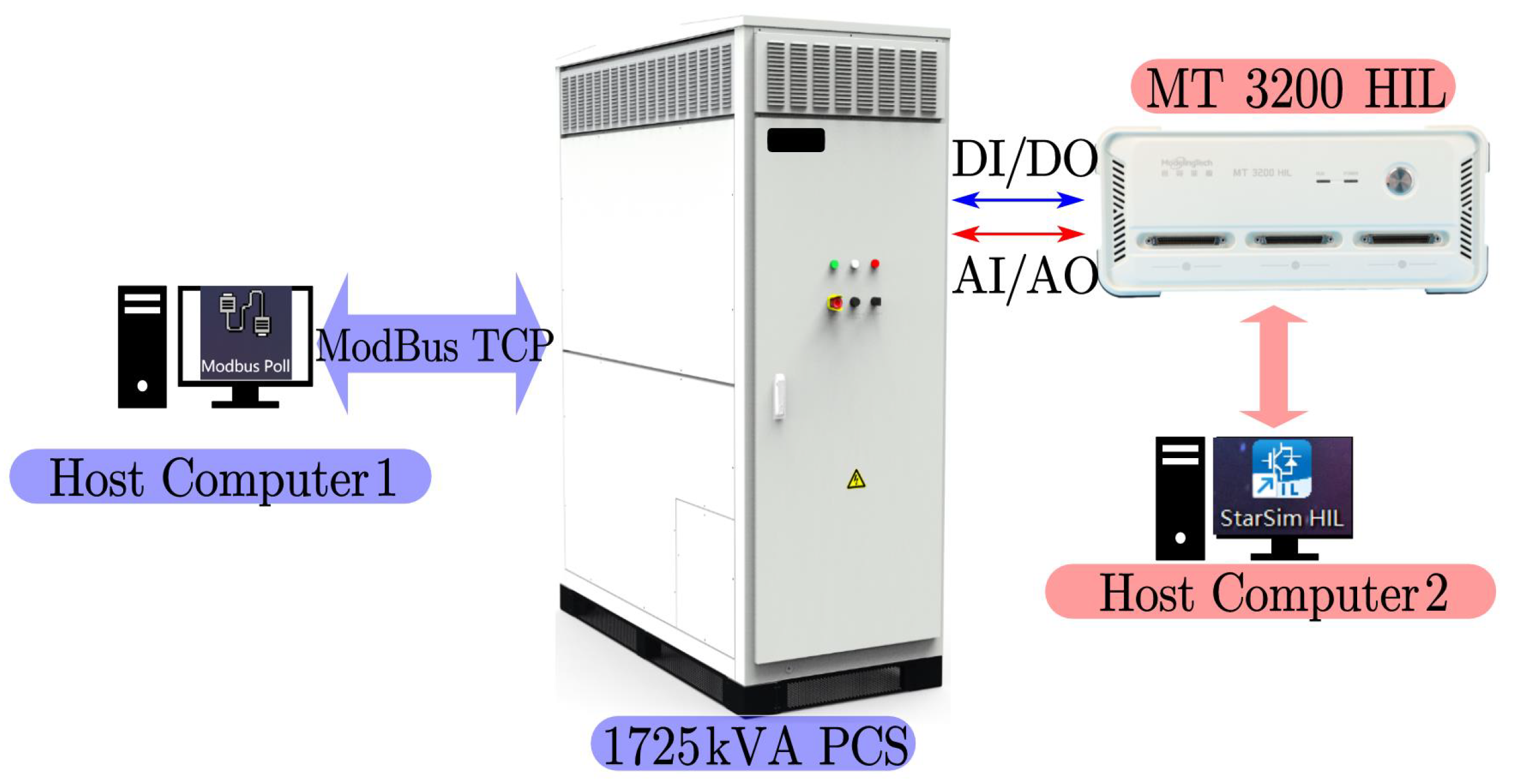
5. Experimental Results

The experiments used ModelingTech MT 3200 HIL to simulate the main power circuit, and the control part used the 1725 kVA PCS control board. Host computer 1 is connected to the 1725 kVA PCS via Modbus, through which commands, such as start/stop/set reference voltage values, can be sent to the PCS. The MT3200 HIL is connected to the PCS via DI/DO and AI/AO connection cables to read values such as PCS voltage, current, and switch signals. Host computer 2 serves as the upper computer of the MT3200 HIL, allowing for the modification of different load types and the monitoring of system voltage and current. The experimental hardware setup is shown in Figure 10. For the details of the PI control in the comparison experiments, see Appendix B.

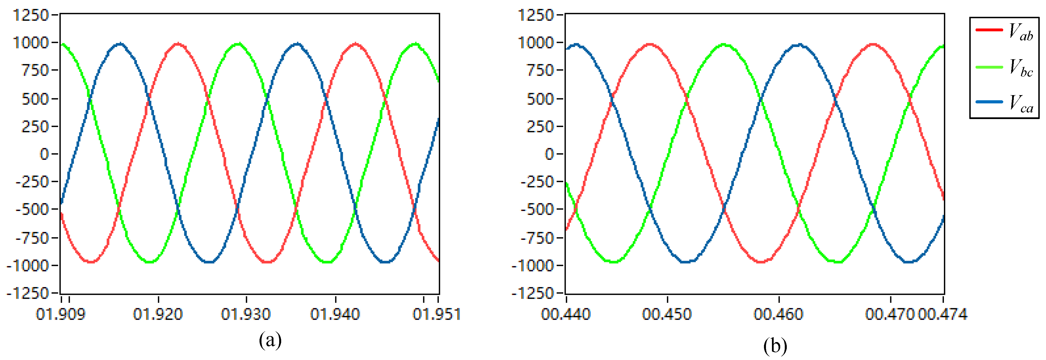
5.1. No-Load Experiment

Figure 11, Figure 12 and Figure 13 show the output voltage waveforms and the THD analysis under PI control and the proposed FRC control, respectively. Analyzing the THD, it can be seen that the proposed control strategy has a very low DC component (less than 0.05%), whereas the DC component using PI control is as high as about 1%; at the same time, the THD of the proposed controller’s output voltage is only half that of the PI control.

5.2. Full-Load Experiment

Figure 14, Figure 15 and Figure 16 show the output voltage waveforms and the THD analysis under the PI control and the proposed FRC control, respectively.
At full load, it is difficult to distinguish the output voltage waveforms of the PI control and the proposed FRC control by the naked eye. This is because the experiments were conducted under very standard conditions. However, in practice, quantitative comparisons can be made through THD analysis. Analyzing the THD from Figure 15 and Figure 16, the experimental results fully demonstrate that the proposed FRC control has a lower DC component (the DC component is close to zero, while the DC component of the PI control is about 1%) and a lower THD (0.38%) compared to the PI control (0.8%).

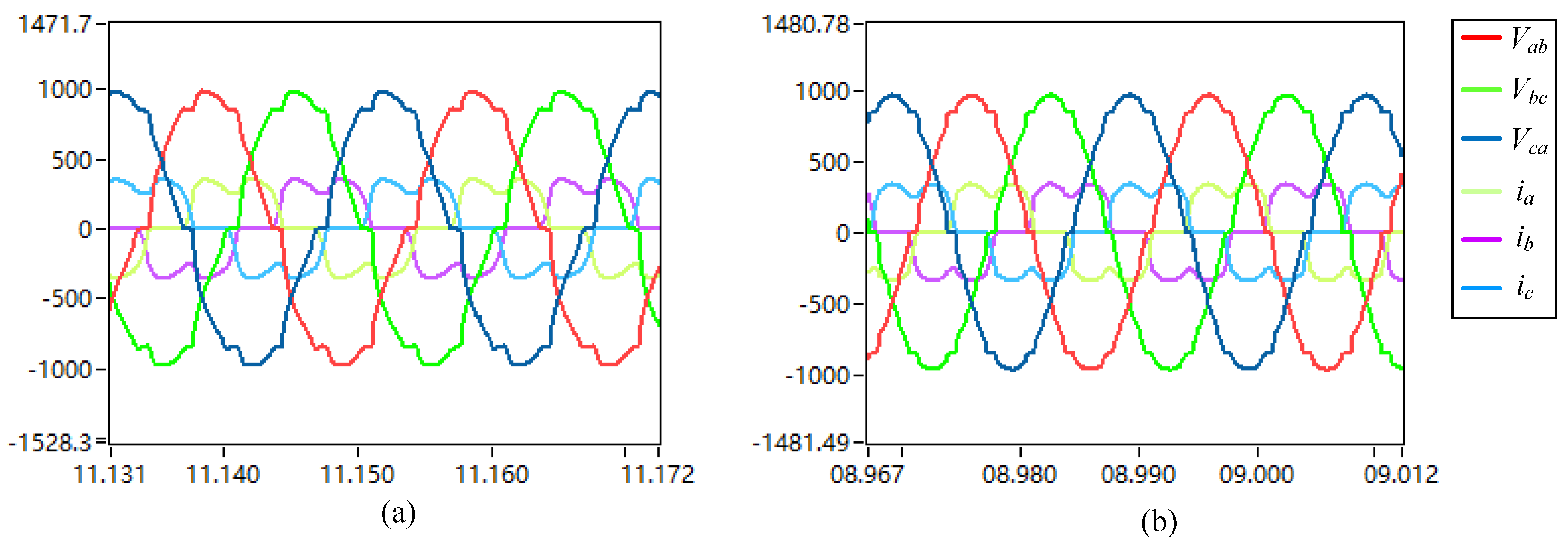
5.3. Nonlinear Load Experiment

The above two sections discussed resistive loads; in order to further explore the harmonic suppression capability of the proposed FRC control, we accessed a 300 kW nonlinear load (which consists of a three-phase uncontrolled rectifier; refer to Appendix D for details), and the output voltages of the PI control and the proposed FRC control are shown in Figure 17. The output voltage THD was analyzed, as shown in Figure 18 and Figure 19.
Observing Figure 17, it is easy to see that the output voltage waveform of the proposed FRC control is smoother and closer to the sinusoidal waveform.
Observing Figure 18 and Figure 19, the THD of the output voltage obtained by FFT analysis is also smaller; the THD of the output voltage of the proposed FRC control is only 3.26%, while the THD of the output voltage using PI is as high as 7.79%. We focused on the THD and found that the output voltage has the fifth harmonic (PI control > 4%, proposed FRC < 1%); seventh harmonic (PI control > 3%, proposed FRC < 0.6%); eleventh harmonic (PI control > 2.5%, proposed FRC < 1.5%) and thirteenth harmonic (PI control > 2%, proposed FRC < 0.7%), and by observing the content of these harmonics, we again prove that the proposed FRC control has better harmonic suppression capability.

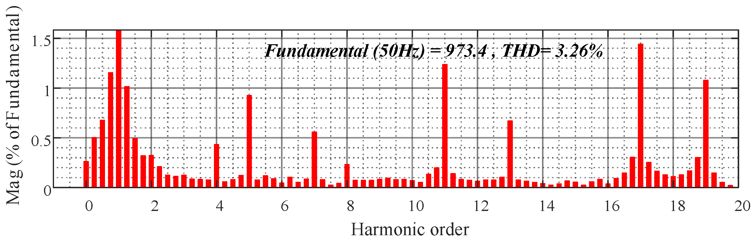
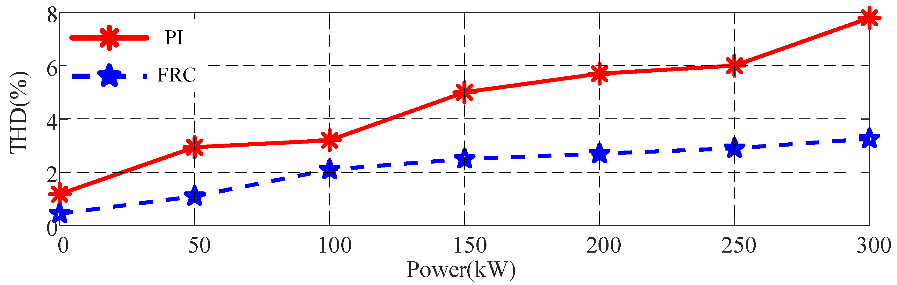
5.4. Output-Voltage Harmonics Comparison

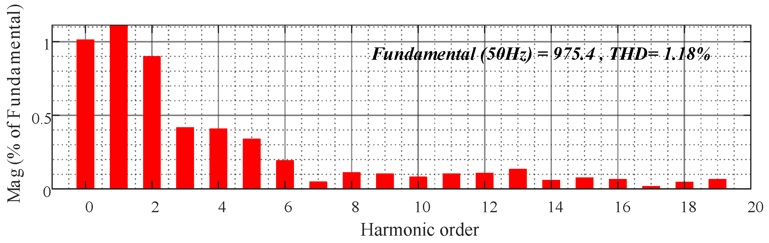
  • To visualize the harmonic suppression capability, the output voltage THD (with resistive loads) at different power levels is shown in Figure 20. The red color represents the PI control, and the blue color represents the FRC control. We take the rated power of 0.1 pu as the step point from zero load to full load. No matter what power level, the proposed output voltage THD content of the FRC control is lower than that of the PI. The THD of the FRC control is approximately 0.5%, which is much lower than the international standard requirements (3%).
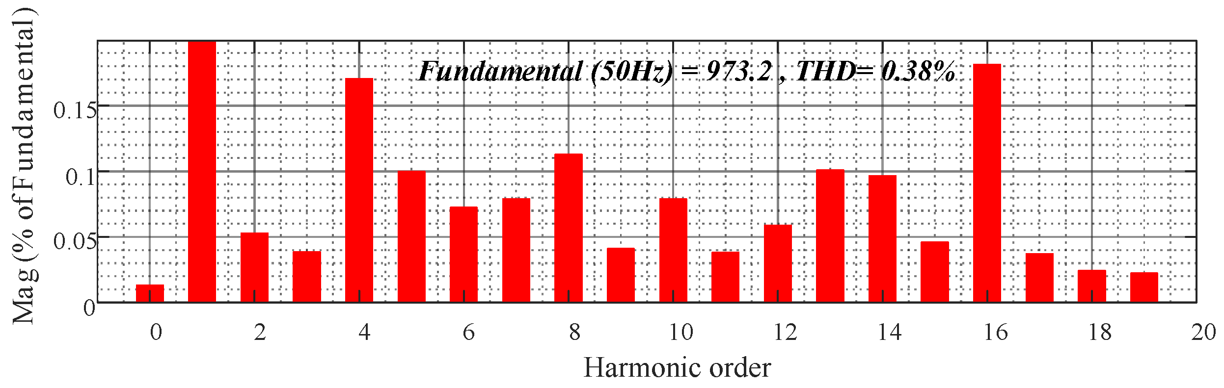
  • To further demonstrate the harmonic rejection capability of the FRC, its output voltage THD (nonlinear load) is shown in Figure 21. With an increasing nonlinear load power (the step unit is 50 kW), the output voltage waveforms of the PI control and FRC control have a certain degree of distortion. The proposed FRC control is capable of suppressing the voltage harmonics to less than 4%, while the PI control is already close to 8%.

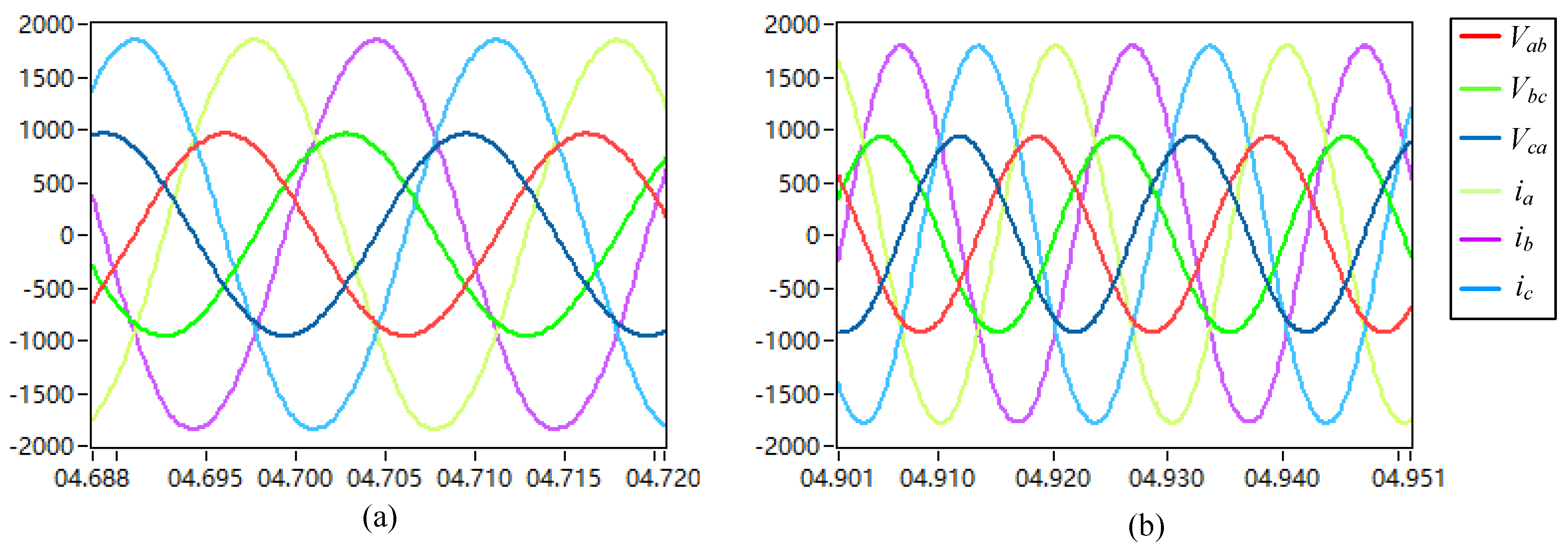
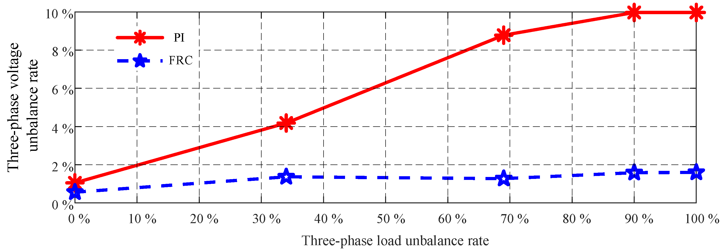
5.5. Three-Phase Unbalanced Load Experiment

In order to verify that the proposed FRC control has the ability to carry 100% of the unbalanced load, we set the three-phase unbalanced load conditions: A-phase heavy load, B-phase light load, and C-phase without load.
Figure 22 shows the PI control and FRC control output voltage waveforms. It can be clearly seen that, by using the FRC control, under the unbalanced load conditions, the output voltage is still in a good balance. However, with PI control, the output voltages show a huge imbalance (one of the peak voltages is over 1000 V, and the other peak voltage is less than 900 V).
To further verify that the proposed FRC control has the ability to carry an unbalanced load, the A/B phase load is set as a heavy load, the C phase load is gradually reduced from a heavy load to a light load, and finally, the C phase is unloaded.
Figure 23 shows the phase voltage unbalance ratio of the PI control and the proposed FRC control as the load changes. The definition and calculation of load unbalance and voltage unbalance are provided in Appendix A.2.
According to Figure 23, we can see that the voltage unbalance ratio (PI control) increases as the load unbalance rate increases, while in the proposed FRC control, the voltage unbalance is not affected by the load change. This again shows that the proposed FRC control has the ability to carry a 100% unbalanced load.

6. Discussion

This paper proposes a voltage loop-control technique for a PCS, which can be applied to the V / f mode and the GFM mode (Refer to Appendix C for details). The advantages of the proposed control are its simple design and easy engineering implementation. The experimental results demonstrate that the proposed FRC control has better harmonic suppression capability and a stronger ability to handle unbalanced loads. Under resistive load conditions, the output voltage THD is always less than 0.5%, which is approximately a 50% reduction in harmonics compared to PI control. Under nonlinear load conditions, the maximum output harmonic of the proposed FRC control is about 3%, while PI control results in about 8% harmonics. Under nonlinear load conditions, the proposed FRC control achieves a maximum output voltage imbalance of less than 2%, while PI control results in a maximum output voltage imbalance of up to 10%.
The proposed control strategy can achieve output voltage harmonic suppression at 100% with unbalanced loads in three phases. However, there are several issues that need to be discussed.
  • In this work, both the V / f mode and GFM mode are based on the voltage single loop to design the controller without considering the current inner loop. Although this design is simple and convenient for engineers to design and debug, the disadvantage is also obvious: in the case of overcurrent, due to the lack of a current inner loop, it is not possible to effectively limit the fault current. However, we believe that this is not an obvious disadvantage for GFM control, and it has been confirmed that the stability of GFM with single-voltage closed-loop control is higher than that of GFM with dual closed-loop control under a robust power grid.
  • In this work, using the V / f control as an example, it has been clearly demonstrated that the proposed controller has excellent control performance. However, in the GFM mode, more tests are needed. The focus of the test should be on whether the proposed controller has a faster voltage response than the PI control. This response speed directly determines the reactive current of the PCS at LVRT/HVRT.
    Theoretically, the proposed voltage controller provides real-time control, while the PI control needs to convert V a b c to V d and V q , and this link usually adds filters to smooth V d and V q . Therefore, the proposed FRC controller should have a faster control speed in GFM mode, and the response speed should be faster than the PI control in the LVRT/HVRT test.
  • The proposed FRC control can be redesigned into a current controller that can be used for the current control of a PCS (e.g., P Q mode or AC constant current mode), and this control can achieve very low grid-connected harmonic currents.
  • If it is desired to add a current inner loop to the FRC control discussed in this work, we strongly do not recommend adding a controller with a similar structure of repetitive control, because it will exacerbate the computational burden of the DSP control chip (for the FRC control, we used 50 kHz; however, we found that the control algorithm could not be calculated in an interrupt cycle in DSP28335, so, we later changed to 40 kHz or adopted an ORC kernel, which solved the problem). PR or QPR control can be used as the current inner loop; however, the stability would need to be re-evaluated.

Author Contributions

Conceptualization, Y.S.; methodology, Y.S.; software, Y.S.; validation, Y.S., S.C. and J.Z.; formal analysis, Y.S. and T.L.; investigation, J.Z.; resources, J.Z.; data curation, S.C. and T.L.; writing—original draft preparation, Y.S.; writing—review and editing, S.C. and T.L.; visualization, Y.S.; supervision, J.Z.; project administration, J.Z.; funding acquisition, J.Z. All authors have read and agreed to the published version of the manuscript.

Funding

This paper was supported by the National Key R&D Program of China (No. 2021YFE0103800).

Data Availability Statement

The experimental data are subject to a confidentiality agreement with the company; however, we have open sourced our simulations as well as code generation related files, which can be accessed at the following website: https://ww2.mathworks.cn/matlabcentral/profile/authors/17710614 (accessed on 10 March 2024).

Acknowledgments

We thank ModelingTech, who provided hardware in the loop test equipment MT3200 HIL.

Conflicts of Interest

The authors declare no conflicts of interest.

Abbreviations

The following abbreviations are used in this manuscript:
PCSpower conversion system
ANPCActive Neutral Point Clamped
RCrepetitive control
PIProportional–Integral
FRCfast repetitive control
VSGVirtual Synchronous Generator
IPMIntelligent Power Module
SFO-PWMSwitching Frequency Optimal-PWM
THDTotal Harmonic Distortion
puper unit
GFMGrid Forming
LVRTLow-Voltage Ride Through
HVRTHigh-Voltage Ride Through
ORCodd repetitive control
PRProportional Resonant
QPRQuasi-Proportional Resonance
DSPDigital Signal Processing
3P3L3 Phase 3 Line
LCURLine Current Unbalance Ratio
PVURphase voltage unbalance ratio
RMSRoot Mean Square
LPFlow-pass filter
PCCpoint of common coupling
HILhardware in the loop
DIDigital Input
DODigital Output
AIAnalog Input
AOAnalog Output
V/fvoltage/frequency

Appendix A

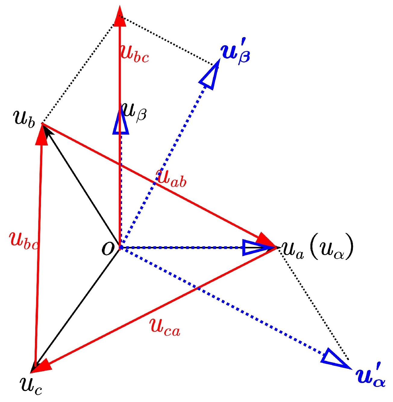
Appendix A.1. 3P3L System with 3/2 Constant Amplitude Transformation Derivation

Since this PCS is a 3P3L system, the 3/2 constant amplitude transformation is selected to carry out the transformation. The equation below can be obtained.
Figure A1. The 3/2 constant amplitude transformation schematic.
Electronics 13 01186 g0a1
u a b = U α u b c = 3 2 U β 1 2 U α
By sorting (A1), (A2) can be obtained:
U α = u a b U β = 1 3 u a b + 2 u b c

Appendix A.2. Three-Phase Load Unbalance Rate Calculation Formula

Three-phase load unbalance rate calculation formula: Assume that the three-phase currents (RMS value) are I a , I b , and I c . The calculation formula for the load unbalance rate is
LCUR = max I a , I b , I c min I a , I b , I c max I a , I b , I c × 100 % .
Assume that the three-line voltages (RMS value) are V a b , V b c , and V c a . The voltage unbalance rate calculation formula is
PVUR = max U ab U avg , U bc U avg , U ca U avg U avg × 100 % .

Appendix B

This appendix contains control diagrams showing the PI control. The PI control was set up as a comparison group for the experiment.
Figure A2. Block diagram using PI control in V / f mode.
Electronics 13 01186 g0a2
The formula for the voltage peak calculation is
v p e a k = u α 2 + u β 2 .
The formula for the calculation of the pu block is 2 / s q r t ( 3 ) / u d c .

Appendix C

Here, we show the application of the FRC control applied to the GFM mode; the experiments showed that the proposed FRC control can be applied to the GFM mode, can work normally in both off-grid and grid-connected conditions, and has the same ability to regulate the voltage amplitude and frequency of the PCC point, as well as the related inertia support. For the relevant test report, the authors can be contacted via email.
Figure A3. Block diagram using FRC control in GFM mode (VSG).
Electronics 13 01186 g0a3

Appendix D

The nonlinear load applied in the paper is shown in the figure.
Figure A4. Nonlinear load.
Electronics 13 01186 g0a4

Appendix E

The code for writing the Butterworth low-pass filter using MATLAB is given below:
% System input;
n = 2; % Filter Order;
wc = 800; % Set Cutoff Frequency;.
fsw = 3600; % Set Switch Frequency;
wn = wc*2/fsw;
[B,A] = butter(n,wn);
S1 = tf(B,A,1/fsw); % A is Denominator; B is Numerator.

References

  1. Guo, J.; Ma, S.; Wang, T.; Jing, Y.; Hou, W.; Xu, H. Challenges of developing a power system with a high renewable energy proportion under China’s carbon targets. iEnergy 2022, 1, 12–18. [Google Scholar] [CrossRef]
  2. Breyer, C.; Khalili, S.; Bogdanov, D.; Ram, M.; Oyewo, A.S.; Aghahosseini, A.; Gulagi, A.; Solomon, A.A.; Keiner, D.; Lopez, G.; et al. On the History and Future of 100% Renewable Energy Systems Research. IEEE Access 2022, 10, 78176–78218. [Google Scholar] [CrossRef]
  3. Zhang, D.; Du, M.; Zhang, Z.; Li, J.; Li, C.; Liu, H.; Shao, L. Effect of multi-energy storage systems on improving the synergy of integrated energy system. In Proceedings of the 2023 3rd New Energy and Energy Storage System Control Summit Forum (NEESSC), Mianyang, China, 26–28 September 2023; pp. 90–93. [Google Scholar]
  4. Chen, X.; Chen, Y.; Lin, Z.; Mao, X.; Chen, J.; Zhang, Z. Design of High-Power Energy Storage Bidirectional Power Conversion System. In Proceedings of the 2020 24th International Conference Electronics, Palanga, Lithuania, 15–17 June 2020; pp. 1–6. [Google Scholar]
  5. Zhai, H.; Yang, F.; Xu, Y.; Liu, J.; Huang, L.; Liu, T.; Hao, X. Performance analysis of VSG controlled PCS in Island mode. In Proceedings of the The 16th IET International Conference on AC and DC Power Transmission (ACDC 2020), Online, 2–3 July 2020; pp. 1042–1045. [Google Scholar]
  6. Zhong, Q.-C.; Weiss, G. Synchronverters: Inverters That Mimic Synchronous Generators. IEEE Trans. Ind. Electron. 2011, 58, 1259–1267. [Google Scholar] [CrossRef]
  7. Rosso, R.; Wang, X.; Liserre, M.; Lu, X.; Engelken, S. Grid-Forming Converters: Control Approaches, Grid-Synchronization, and Future Trends—A Review. IEEE Open J. Ind. Appl. 2021, 2, 93–109. [Google Scholar] [CrossRef]
  8. Zhou, J.; Zhang, R.; Zhang, X.; Wu, J.; Huang, W. A Compound Control Strategy for Inverter Output Voltage in Micro-grid System. In Proceedings of the 2018 IEEE 4th Southern Power Electronics Conference (SPEC), Singapore, 10–13 December 2018; pp. 1–5. [Google Scholar]
  9. Zhang, Z.; Zhang, D.; Ma, J.; Lu, H.; Zhou, Y.; Xi, Z. Based on Vector Proportional Integral (VPI) Control of Brushless Doubly Fed Induction Generator under Load Imbalance. In Proceedings of the 2022 4th Asia Energy and Electrical Engineering Symposium (AEEES), Chengdu, China, 25–28 March 2022; pp. 64–70. [Google Scholar]
  10. Fantino, R.A.; Busada, C.A.; Solsona, J.A. Optimum PR Control Applied to LCL Filters with Low Resonance Frequency. IEEE Trans. Power Electron. 2018, 33, 793–801. [Google Scholar] [CrossRef]
  11. Nazeri, A.A.; Saeidi, M.; Zacharias, P. Design and Performance Analysis of a Modified Proportional Multi-Resonant (PMR) Controller for Three-Phase Voltage-Source Inverters. In Proceedings of the 2022 24th European Conference on Power Electronics and Applications, Hanover, Germany, 5–9 September 2022; pp. 1–12. [Google Scholar]
  12. Rahman, M.M.; Biswas, S.P.; Islam, M.R.; Muttaqi, K.M.; Muyeen, S.M. Design of a High Performance Resonant Controller for Improved Stability and Robustness of Islanded Three-Phase Microgrids. IEEE Access 2022, 10, 119206–119220. [Google Scholar] [CrossRef]
  13. Sun, Y.; Zhou, J. Grid-Tied Inverter Fractional-Order Phase Compensation via Odd Repetition Control. In Proceedings of the International Conference on Electrical Engineering and Green Energy (CEEGE), Grimstad, Norway, 6–9 June 2023; Volume 10, pp. 62–68. [Google Scholar]
  14. Xu, J.; Soeiro, T.B.; Gao, F.; Chen, L.; Tang, H.; Bauer, P.; Dragičević, T. Carrier-Based Modulated Model Predictive Control Strategy for Three-Phase Two-Level VSIs. IEEE Trans. Energy Convers. 2021, 36, 1673–1687. [Google Scholar] [CrossRef]
  15. Andino, J.; Ayala, P.; Llanos-Proaño, J.; Naunay, D.; Martinez, W.; Arcos-Aviles, D. Constrained Modulated Model Predictive Control for a Three-Phase Three-Level Voltage Source Inverter. IEEE Access 2022, 10, 10673–10687. [Google Scholar] [CrossRef]
  16. Pardhi, P.K.; Sharma, S. Implementation of Robust Controller for VSI Feeding Stand-alone Loads. In Proceedings of the 2019 IEEE 1st International Conference on Energy, Systems and Information Processing, Chennai, India, 4–6 July 2019; pp. 1–5. [Google Scholar]
  17. Sun, Y.; Zhao, Q.; Liao, W.; Jiang, K.; Tan, W. Robust Repetitive Controller Design Based on S/SK Problem for Single-phase Grid-connected Inverters. In Proceedings of the International Conference on Robotics and Automation Engineering (ICRAE), Guangzhou, China, 19–22 November 2021; pp. 223–230. [Google Scholar]
  18. Vieira, R.P.; Martins, L.T.; Massing, J.R.; Stefanello, M. Sliding Mode Controller in a Multiloop Framework for a Grid-Connected VSI With LCL Filter. IEEE Trans. Ind. Electron. 2018, 65, 4714–4723. [Google Scholar] [CrossRef]
  19. Shen, X.; Wu, C.; Liu, Z.; Wang, Y.; Leon, J.I.; Liu, J.; Franquelo, L.G. Adaptive-Gain Second-Order Sliding-Mode Control of NPC Converters Via Super-Twisting Technique. IEEE Trans. Ind. Electron. 2023, 38, 15406–15418. [Google Scholar] [CrossRef]
  20. Rodrguez, J.; Lai, J.; Peng, F. Multilevel inverters: A survey of topologies controls and applications. IEEE Trans. Ind. Electron. 2002, 49, 724–738. [Google Scholar] [CrossRef]
  21. Barater, D.; Concari, C.; Buticchi, G.; Gurpinar, E.; De, D.; Castellazzi, A. Performance Evaluation of a Three-Level ANPC Photovoltaic Grid-Connected Inverter With 650-V SiC Devices and Optimized PWM. IEEE Trans. Ind. Appl. 2016, 52, 2475–2485. [Google Scholar] [CrossRef]
  22. Barbosa, P.; Steimer, P.; Meysenc, L.; Winkelnkemper, M.; Steinke, J.; Celanovic, N. Active Neutral-Point-Clamped Multilevel Converters. In Proceedings of the IEEE 36th Power Electronics Specialists Conference, Dresden, Germany, 16 November 2005; pp. 2296–2301. [Google Scholar]
  23. Taallah, A.; Mekhilef, S. Active neutral point clamped converter for equal loss distribution. IET Power Electron. 2014, 7, 1859–1867. [Google Scholar] [CrossRef]
Figure 1. Single-stage ANPC three-level circuit topology.
Electronics 13 01186 g001
Figure 2. Bode diagram of the controlled object P ( z ) .
Electronics 13 01186 g002
Figure 3. Block diagram of the proposed FRC.
Electronics 13 01186 g003
Figure 4. Control block of the inverter system.
Electronics 13 01186 g004
Figure 5. P ( z ) root trajectory diagram.
Electronics 13 01186 g005
Figure 6. Bode diagram of P 0 ( z ) with different k p .
Electronics 13 01186 g006
Figure 7. Bode plot of zero-phase low-pass filter Q when α 0 is taken as 2/4/6.
Electronics 13 01186 g007
Figure 8. z m S ( z ) P 0 ( z ) Phase frequency characteristic curve.
Electronics 13 01186 g008
Figure 9. Open−loop Bode plot of G F R C .
Electronics 13 01186 g009
Figure 10. Experimental environment.
Electronics 13 01186 g010
Figure 11. (a) PI control no−load output voltage waveform; (b) proposed FRC control no−load output voltage waveform.
Electronics 13 01186 g011
Figure 12. PI control no−load output voltage THD analysis.
Electronics 13 01186 g012
Figure 13. Proposed FRC control no−load output voltage THD analysis.
Electronics 13 01186 g013
Figure 14. (a) PI control full−load output voltage waveform; (b) proposed FRC control full−load output voltage waveform.
Electronics 13 01186 g014
Figure 15. PI control full-load output voltage THD analysis.
Electronics 13 01186 g015
Figure 16. Proposed FRC control full-load output voltage THD analysis.
Electronics 13 01186 g016
Figure 17. (a) PI control with 300 kW nonlinear load output voltage waveform; (b) proposed FRC control with 300 kW nonlinear load output voltage waveform.
Electronics 13 01186 g017
Figure 18. PI control with 300 kW nonlinear load output voltage THD analysis.
Electronics 13 01186 g018
Figure 19. Proposed FRC control with 300 kW nonlinear load output voltage THD analysis.
Electronics 13 01186 g019
Figure 20. Output voltage THD at different power levels (with resistive loads).
Electronics 13 01186 g020
Figure 21. Output voltage THD at different power levels (with nonlinear loads).
Electronics 13 01186 g021
Figure 22. (a) PI control with unbalanced load output voltage waveform; (b) proposed FRC control with unbalanced load output voltage waveform.
Electronics 13 01186 g022
Figure 23. Three-phase voltage unbalance ratio at different load unbalance ratios.
Electronics 13 01186 g023
Table 1. 1725 kVA PCS system parameters.
DC Characteristics
Maximum DC voltage1500 Vdc
Minimum DC voltage1000 Vdc
Full load DC operating voltage range1000–1500 Vdc
Maximum DC current1935 A
AC Characteristics (Off-Grid)
Nominal output power1725 kVA
Maximum output current1578 A
Nominal AC voltage690 Vac
AC voltage range−15%–10%
AC voltage harmonics<3% (Linear loads)
DC voltage components<0.5% × Un
Nominal frequency/frequency range50 Hz/45∼55 Hz
Overload capacity120% (20 s)
Number of phases at the output3 phases/3 lines
Table 2. Parameters of the main circuit of a PCS.
ParametersValue
Filter inductor DC resistance: R0.35 Ω
Filter inductors: L0.07 mH
Filter capacitor: C*240 μF
C* is the equivalent filtering capacitor after series–parallel connection (C* = 3Cf).
Table 3. Parameters of the FRC.
ParametersValue
N72
z m z 2
Q z + 2 + z 1 4  
S ( z ) 0.3459 z 2 + 0.6919 z + 0.3459 z 2 + 0.2047 z + 0.179
Disclaimer/Publisher’s Note: The statements, opinions and data contained in all publications are solely those of the individual author(s) and contributor(s) and not of MDPI and/or the editor(s). MDPI and/or the editor(s) disclaim responsibility for any injury to people or property resulting from any ideas, methods, instructions or products referred to in the content.

