Article

A Novel Single-Phase Five-Level Current-Source Inverter Topology

by
Mayas Fakher Aldin
and
Kfir Jack Dagan
*
Department of Electrical and Electronics Engineering, Ariel University of Samaria, Ariel 40700, Israel
*
Author to whom correspondence should be addressed.
Electronics 2024, 13(7), 1213; https://doi.org/10.3390/electronics13071213
Submission received: 11 February 2024 / Revised: 17 March 2024 / Accepted: 22 March 2024 / Published: 26 March 2024
(This article belongs to the Special Issue New Trends in Power Electronics for Microgrids)

Abstract

:
Recent technological advances have renewed the research interest in current-source inverters (CSIs). Nonetheless, CSI research still falls behind its voltage-source counterpart with regards to topologies, modulation, and control. Acknowledging the above, this paper presents a novel single-phase five-level CSI topology. The proposed circuit utilises eight switches and two inductors for the generation of five distinct output levels while maintaining low output voltage THD and d v / d t . Furthermore, by offsetting the inductor currents from a binary 1:2 to a trinary 1:3 ratio, the proposed inverter can generate seven current levels at its output. The inverter offers built-in short-circuit protection and can boost a low input DC voltage to a higher peak AC output voltage. These merits, alongside an electrolytic-capacitor-free design, simple current balancing mechanism, and fault-tolerant characteristics, make it a promising candidate for PV module-integrated inverter (MII) systems. The current topology utilises two inductors but is fully functional with single-inductor operation. The paper provides a functional analysis of the inverter topology alongside the inverter switching states and corresponding conduction paths. A detailed analysis of the inductor current dynamics as well as a current-balancing algorithm for dual- and single-inductor operations are given. The theoretical analysis of the proposed circuit and its functional operation are verified using simulations and experimental results carried out on a laboratory prototype.

1. Introduction

Converter topologies can be generally divided into two groups: namely, voltage-source inverters (VSIs) and current-source inverters (CSIs) [1,2]. Traditionally, superior efficiency and structural simplicity have tipped the research scale in favour of voltage-fed inverters [3] and have left CSIs lagging behind with respect to topologies, control methods, modulation strategies, and modelling [4]. Wide industry adoption of VSIs has, in turn, influenced the semiconductor market, resulting in enhancement-mode devices that lack reverse-blocking (RB) capabilities [5]. This has further consolidated the role of VSIs in the power conversion arena and has limited CSI applications to high-power, low-switching-frequency conversion [6,7,8].
However, recent advances in semiconductor technology have opened new avenues for CSI applications. Wide bandgap (WBG) devices facilitate switching frequencies an order of a magnitude higher compared with their Si counterparts and are capable of withstanding higher junction temperatures [9]. Increased switching frequencies result in notable volume reduction of DC link inductors and lead to higher converter power densities. This is not necessarily the case with VSIs, for which DC link capacitors are mostly sized to withstand current ripples [10]. Increased system operating temperature, made possible through a combination of high-temperature-resilient inductors and WBG devices with increased junction temperatures, can ease cooling requirement and result in even denser converters. Finally, the emergence of single-chip RB-IGBTs [11] and fabrication progress made with their WBG siblings, RB-SiC [12] and RB-GaN [13], is expected to further improve CSI densities by reducing package count and minimizing parasitic inductance.
Industry trends towards higher-performance systems, mainly in terms of efficiency, power density, reliability, and lifespan, also encourage the re-evaluation of traditional converter configurations. CSIs’ inherent voltage boosting characteristics, electrolytic-capacitor-free design, and low output voltage to total harmonic distortion (THD) are all highly desirable features, which if taken into account during the design stage, can make CSIs a leading candidate in many power conversion applications [14].
Solar photovoltaic (PV) systems are a distinct domain in which CSI conversion can prove beneficial. Binding energy targets necessitate improved PV systems with increased returns on investment (ROIs) [15]. Voltage-fed PV inverters employ aluminium electrolytic capacitors (AEC) that degrade system reliability and increase downtime and maintenance costs [16]. CSIs, on the other hand, use power inductors capable of withstanding harsh thermal cycles and match the lifespan of PV modules: namely, 25 years [17,18,19]. Matching the lifetime of PV modules is extremely important for module-integrated inverter (MII) systems, for which power electronics are mounted directly on the module and are exposed to extreme weather conditions [20]. MII systems hold great potential in residential PV applications as they improve energy harvesting [21], increase system efficiency and reliability [17], and lower installation costs [22]. This potential has led to studies on the reliability of power electronics components in a module-mounted environment [23,24]. Power inductors also mitigate DC voltage ripple and, hence, reduce PV module stress [25] and improve the efficacy of maximum power point tracking (MPPT) [26]. An intrinsic voltage boosting characteristic is another distinct advantage of current-fed conversion. It supports the elimination of the DC-DC converter and step-up transformer stages in DC-AC applications wherein the DC voltage is lower than the output AC peak voltage [27]. This is predominantly the case with fuel cells and PV applications [28]. For the latter, voltage boosting lays the foundation for a single-stage transformerless PV-CSI system [29,30]. Moreover, CSIs’ inductive DC link provides short-circuit protection and increases system safety [31,32].
More electric aircraft (MEA) and electric vehicles (EVs) can also benefit from the advancement of CSI technology. In these systems, higher power densities are attained by increasing the electric machine (EM) rotational speed [33]. Increased shaft speed corresponds to a higher motor drive frequency, which in turn results in slimmer DC links. Furthermore, it has been demonstrated that improved performances can be achieved with EMs designed for higher rated voltages. CSIs feature low output voltage THD and favourable d v / d t , which applies less stress on EM terminals and prevents winding insulation ageing [34] and insulation failure [35]. These features, combined with their voltage boosting characteristics, make CSIs a viable choice for low DC voltage transport drives [14].
Other applications that can benefit from CSI integration appear in the literature. Fuel cell stacks feature low output DC voltage that varies according to operating conditions. A single-stage CSI can boost the low output voltage to the higher peak line voltage while regulating the voltage variations [27]. Current-fed conversion has also been proposed for wind turbine power conversion due to its simple configuration, low device count, low d v / d t , reliable short-circuit protection, and inherent four-quadrant operation [36]. Another field in which CSI can prove advantageous is superconducting magnetic energy storage (SMES) systems [37]. SMES systems’ lossless inductive characteristic render them a strong candidate for replacing the traditional CSI DC link. By integrating SMES into CSIs, energy can flow in the absence of lossy power inductors while providing more reactive power compared to VSIs [38]. For similar reasons, the integration of SMES coils has been suggested for CSI-fed wind turbine systems [39]. Finally, the application of CSI-based static synchronous compensators (STATCOMs) has shown to posses a dynamic response comparable to that of VSI while attaining excellent steady-state tracking [40].
Various multilevel single-phase CSIs as well as their application to module-integrated and three-phase PV systems have been covered in the literature, the significance of which are described below. Ref. [41] provides a comprehensive review of CSI-based conversion systems for PV applications. Another study focusing on multi-stage CSI-based grid-connected PV systems is given in [42]. The paper outlays CSIs’ improved gain, performance, energy quality, and lifetime and thereby emphasises their viability in renewable applications. A current-source grid inverter for a hybrid PV and SMES energy system is described in [43]. The hybrid system shares a single CSI, which offers simplified control of the AC side. A three-level CSI topology employing a single inductor, five switches, and a freewheeling diode is proposed in [44]. A SiC-based implementation of this inverter is then presented in [45], wherein system reliability is analysed in light of load overvoltage. Another transformerless single-phase three-level topology is introduced in [46] for PV systems. The proposed CSI mitigates leakage current by coupling the grid neutral line to the negative terminal of the PV panel. Mitigating leakage current in transformerless grid-tied PV systems is of utmost importance, as leakage current may result in grid current distortion, power losses, and safety issues [47]. Another work addressing the same phenomenon is presented in [48], wherein the reduction of ground leakage current is gained by adding auxiliary switches to a fully bridged CSI. A unidirectional n-level CSI cell is presented in [49]. Its five-level configuration employs eight switches and three inductors to generate the desired output levels. An equivalent bidirectional nine-level version of the inverter is shown in [50]. Its reduced bidirectional five-level equivalent circuit can be derived, for which eight switches and two inductors are required to generate a five-level output. Another five-level CSI structure was proposed in [51]; it employs a symmetrical circuit with eight switches and two inductors. The paper also provide a generalised circuit capable of generating n-levels. A three-phase seven-level CSI topology from which a single-phase equivalent circuit can be derived is proposed in [52]. The reduced single-phase topology makes use of four inductors and eight switches to generate five current levels. A simplified topology of the one presented in [49] is proposed in [53]. This topology employs six switches and a single inductor to generate five output levels.
This paper proposes a novel CSI topology utilising eight switches and two inductors for the generation of five distinct current levels. By offsetting the inductor currents from a binary 1 : 2 to a trinary 1 : 3 ratio, the inverter can generate seven output levels. The inverter can also operate in a single inductor mode while generating the same output levels at the cost of increasing the inductor current ripple. Different from the above-mentioned papers, the balancing mechanism for the inductor currents is analysed in detail for both dual- and single-inductor operation. Furthermore, a preliminary analysis of switches’ stress and power loss is given. In order to verify the functional operation of the inverter, a laboratory prototype was developed and tested in an open-loop mode; the results closely match those of the theoretical and simulative analysis.
The rest of the paper is structured as follows: Section 2 presents the proposed CSI circuitry alongside its switching states and corresponding conduction paths. The section also mathematically analyses the dynamics of the inductor currents and provides a mechanism for their balancing. In Section 3, the simulation results of a Simulink/MATLAB model are presented and analysed. Section 4 provides verification of the theoretical and simulation sections in terms of the experimental results. Finally, conclusions emphasizing the main results and advantages of the proposed inverter are given in Section 5.

2. Materials and Methods

Figure 1 shows a schematic of the proposed current-source inverter. As seen in the figure, the inverter consists of two inductors and eight reverse-blocking switches. Each switch is realised using a transistor–diode pair connected in series. Switches S 12 , S 13 , S 22 , and S 23 operate as H-Bridge (HB) converters that reverse the output current at each fundamental half-cycle.

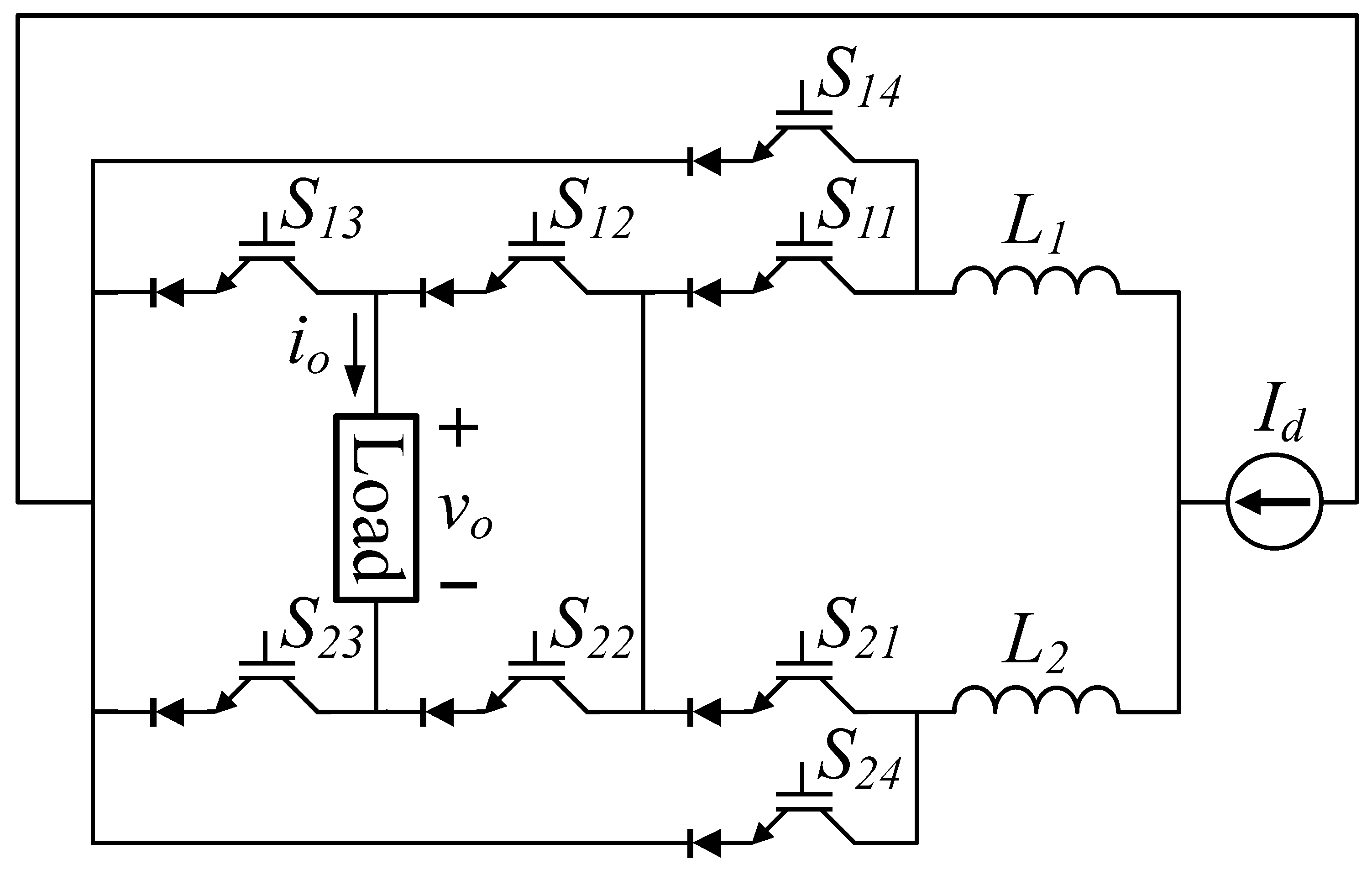
2.1. Inverter Switching States

Table 1 lists the practical switching states of the proposed inverter, while Figure 2 depicts their corresponding conduction paths. An ideal DC current source of magnitude I d is assumed throughout this section. For simplicity’s sake, inductor currents i L 1 and i L 2 are each assumed to carry half the source current I d / 2 .
Figure 2a depicts the conduction path of inverter output current I d . In this state, switches S 11 and S 21 each carry half the source current. The currents are then merged, delivered to the load, and fed back to the source using switches S 12 and S 23 .
Figure 2b depicts one of the two possible conduction paths for output current I d / 2 . Here, inductor current I L 1 is driven to the load via S 11 and S 12 and then fed back to the source via S 23 . Inductor current I L 2 is fed back through S 24 directly to the source. Another switching state delivering I d / 2 to the load is shown in Figure 2c. Similar to the previous state, inductor current I L 2 is fed to the load and back to the source through switches S 21 , S 12 , and S 23 , while inductor current I L 1 is fed back directly to the source through S 14 . The above switching states refer to the positive current half-cycle for which HB switches S 12 and S 23 are on at all times.
The zero-current state is illustrated in Figure 2d. Here, inductor currents I L 1 and I L 2 are fed back to the source through, respectively, switches S 14 and S 24 . It should be noted that the zero-current state is independent of the state of HB switches S 12 , S 13 , S 22 , and S 23 , which can be set according to practical considerations.
The switching states for the negative current half-cycle are shown in Figure 2e–g. Reversing the inverter output current is accomplished by toggling the HB switches so that switches S 12 and S 23 are turned off, while switches S 13 and S 22 are turned on at all times.
Similar to the positive case, output current I d / 2 can be realised using two different switching states. The first state is shown in Figure 2e, whereby inductor current I L 2 is routed through switches S 21 and S 22 to the load and back to the source via S 13 . In this state, inductor current I L 1 is fed back directly to the source via S 14 . Output current I d / 2 can also be attained by turning on switches S 11 , S 22 , and S 13 as shown in Figure 2f. Here, inductor current I L 1 is fed back to the source via S 24 .
Finally, output current I d is realised through the conduction path depicted in Figure 2g. Similar to the positive case, inductor currents i L 1 and i L 1 flow through, respectively, switches S 11 and S 11 , are merged and routed to the load via S 22 , and are fed back to the source through S 13 .
The above analysis relates to binary inverter operation wherein a current of the same magnitude I d / 2 is flowing through inductors i L 1 and i L 2 . By asymmetrically dividing the source current between the inductors such that a trinary current ratio i L 1 : i L 2 = 1 : 3 is obtained, a seven-level CSI is derived. This can be easily deduced by offsetting the inductor currents accordingly and following the analysis given in this section. It is not within the scope of this paper to analyse the means of current offsetting or to analyse the effect on the inverter’s operation in light of it.

2.2. Inductor Current Balancing

For the inverter to operate normally, inductor currents must be balanced within a fundamental cycle. This is maintained by selectively employing the redundant switching states for output currents i o = ± I d / 2 as depicted in Figure 2. From Kirchhoff’s current law, we get
i L 1 + i L 2 = I d
for all switching states illustrated in Figure 2. Applying Kirchhoff’s voltage law to Figure 2b,e yields
v L 1 v L 2 = v o
which results in
L 1 d i L 1 d t L 2 d i L 2 d t = v o
Substituting (1) into (3), the following equation can be derived:
d i L 1 d t = v o L 1 + L 2
Similarly, applying the above analysis to Figure 2c,f, we get
d i L 1 d t = + v o L 1 + L 2
Based on (4) and (5), the following rule for the balancing of inductor currents can be derived:
S 11 = S 24 = 1 + s g n i o s g n v o s g n i L 1 i L 2 2 , i o = ± I d 2
where s g n ( ) denotes the sign function:
s g n x = + 1 x 0 1 x < 0
and S 11 = S 24 = S 21 ¯ = S 14 ¯ for inverter output currents ± I d / 2 .
HB switches are determined according to the output current polarity as follows:
S 12 = S 23 = 1 + s g n i o 2
while S 13 = S 22 = S 12 ¯ = S 23 ¯ regardless of the output current.
It should be noted that the above analysis can be adapted for single-inductor operation of the inverter. In this case, one of the inductors is replaced by a short circuit, while the current of the remaining inductor is balanced to half the source current. Current balancing in single-inductor operation mode follows similar lines to that of the dual-inductor operation described above. In this case, for intermediate current levels i o = ± I d / 2 , the instantaneous load voltage can be applied to a single inductor in either polarity by appropriately selecting between redundant switching states. Thus, (4) and (5) are reduced to
d i L 1 d t = ± v o L 1
where the positive and negative signs correspond to, respectively, Figure 2b,e and Figure 2c,f. The resulting balancing rule then becomes
S 11 = S 24 = 1 + s g n i o s g n v o s g n i L 1 i s 2 2 , i o = ± I d 2
where i s is the instantaneous current supplied by the source. It should be noted that in this case, the single inductor will experience a voltage drop equal in magnitude to the full extent of the instantaneous load voltage. As a result, its current derivative will double, leading to increased current ripple compared to the dual-inductor case.

2.3. Sizing Considerations

While transistor sizing is not within the scope of this paper, it is worth dwelling on two key factors affecting transistor rating: namely, switching frequency and maximum current. As described above, the maximum current carried by HB switches equals the source current I d . Since HB switches determine the polarity of the output current, they commutate at the fundamental frequency: toggling every half-cycle of the output current.
Switch pairs S 11 , S 14 and S 21 , S 24 direct, respectively, inductor currents i L 1 and i L 2 through and away from the load. Hence, they carry a maximum current equal to half the source current I d / 2 . These switches operate at the carrier frequency.
The above characteristics are summarised in Table 2, where f 0 and f Δ denote, respectively, the fundamental and carrier frequencies.
As the power loss of a switch is directly related to the product of the current flowing though it and its switching frequency, the above combination supports a moderate rating choice for both HB and non-HB switches.

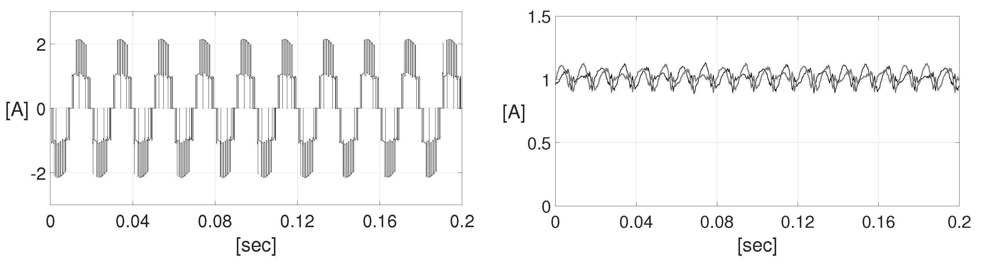
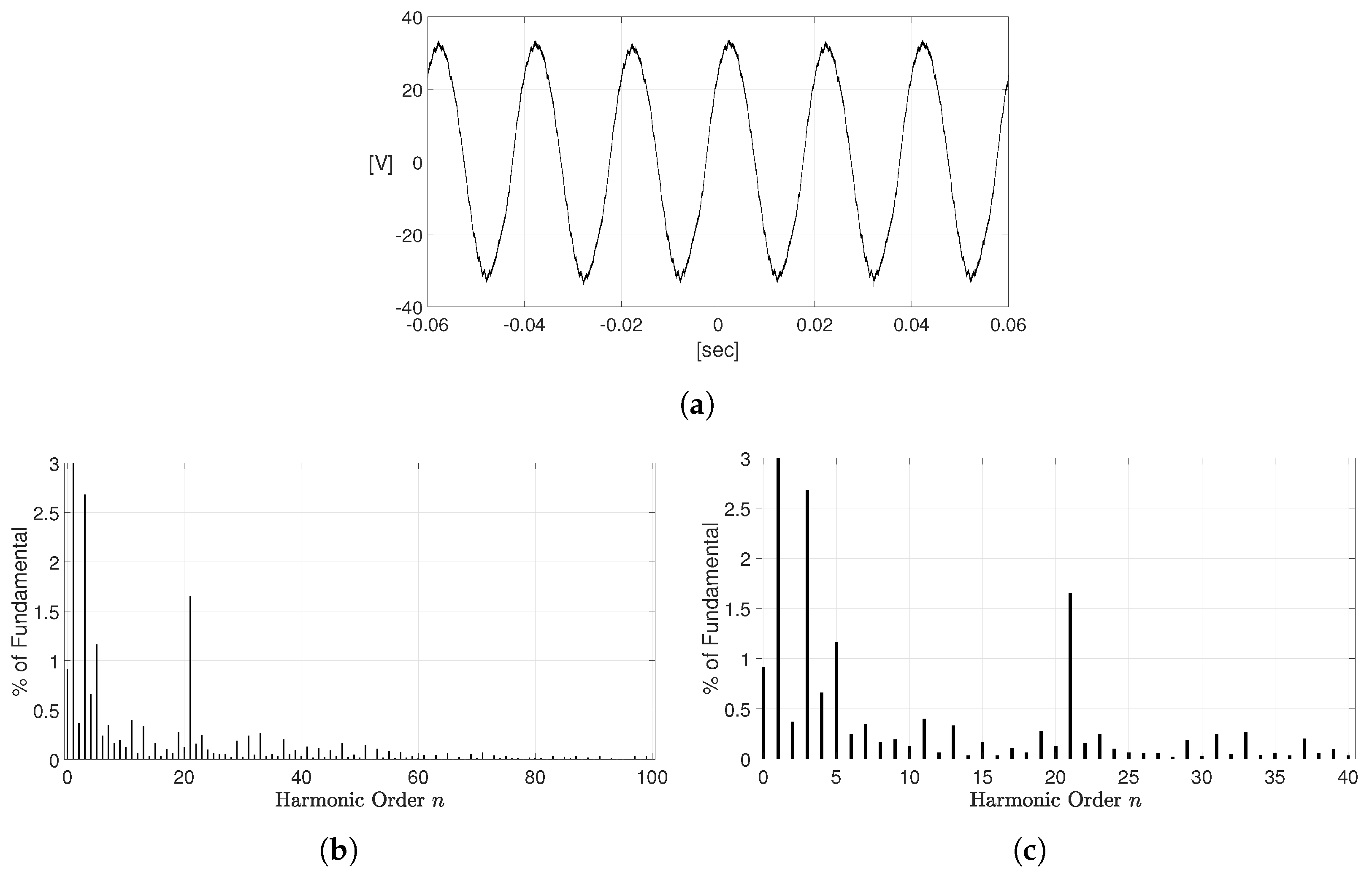
3. Simulation Verification

A Simulink/MATLAB R2023b model was developed to verify the operation of the proposed converter. Sine-PWM (SPWM) was used to generate the gating signals for the various transistors. For simplicity’s sake, the DC current source was implemented using an ideal DC voltage source with a magnitude of 15 V connected in series with a 100 mH inductor. The simulation parameters are summarised in Table 3.
Normal inverter operation requires the balancing of inductor currents i L 1 and i L 2 . This was attained by employing a simple hysteresis control that implemented the balancing rule developed in Section 2.2.
Inverter output current i I N V and inductor currents i L 1 and i L 2 are shown in Figure 3. As expected, the inverter output current features five discrete levels, while inductor currents i L 1 and i L 2 fluctuate around their 1 A DC level.
Figure 4 depicts the load voltage v o in the time and frequency domains. As can be seen in Figure 4a, v o features a sinusoidal waveform with a very low d v / d t and a peak voltage of 30 V. Recalling the 15 V magnitude of the DC source, the amplified output voltage to some extent reflects the voltage boosting capability of the proposed inverter. Analysis of the inverter voltage boosting ratio as well as the modulation scheme for realising it is outside the scope of this paper and will be addressed in a future publication.
The normalised harmonic content of the load voltage is shown in Figure 4b,c. Close examination of these figures reveals two notable features. The first is a dominant harmonic component of the 21st order and with an amplitude of about 1.75 % of the fundamental component. This is coherent with the 1050 Hz carrier frequency listed in Table 3. The second feature is a normalised third harmonic component with an amplitude of 1 % . This is an outcome of a low current oscillation originating from the inverter interaction with the current source (constructed from a DC voltage source in series with a choke inductor). The load voltage THD index was 2.28 % .

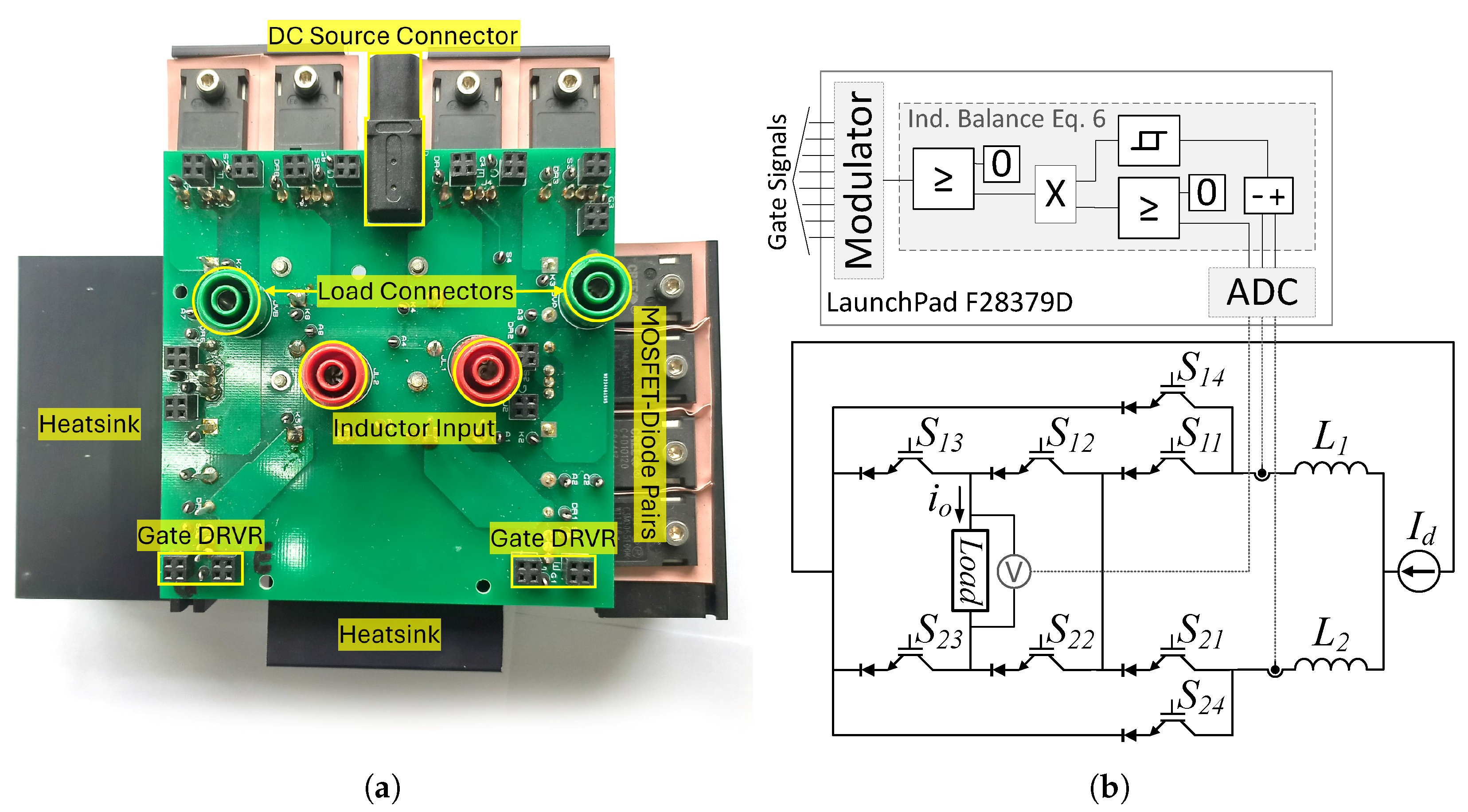
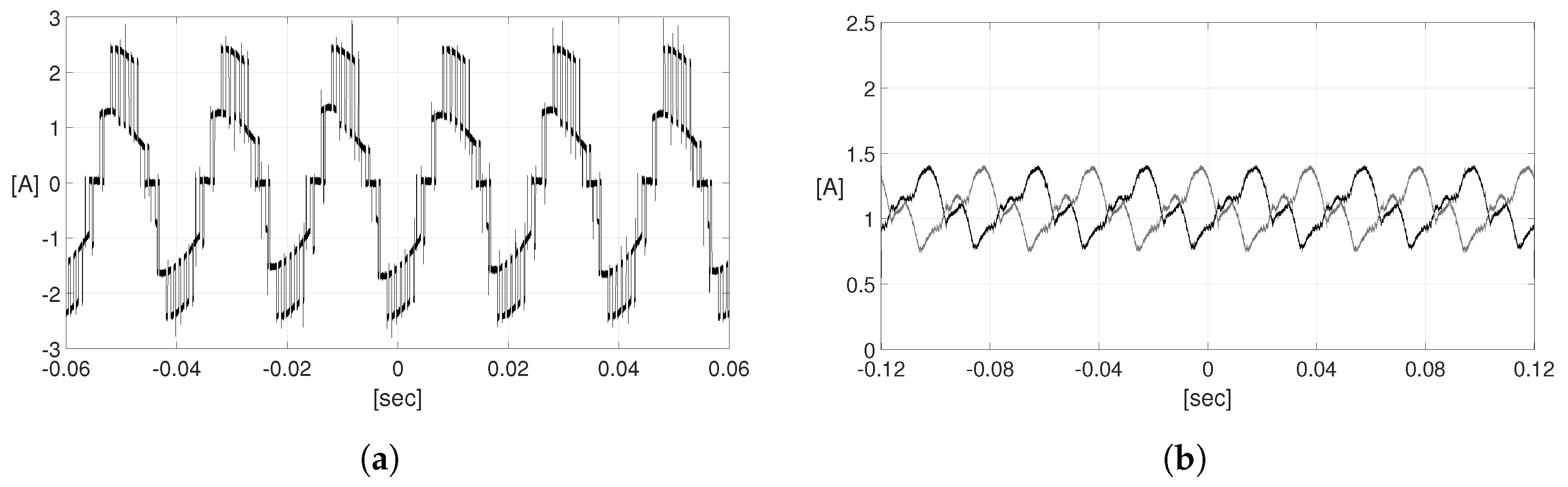
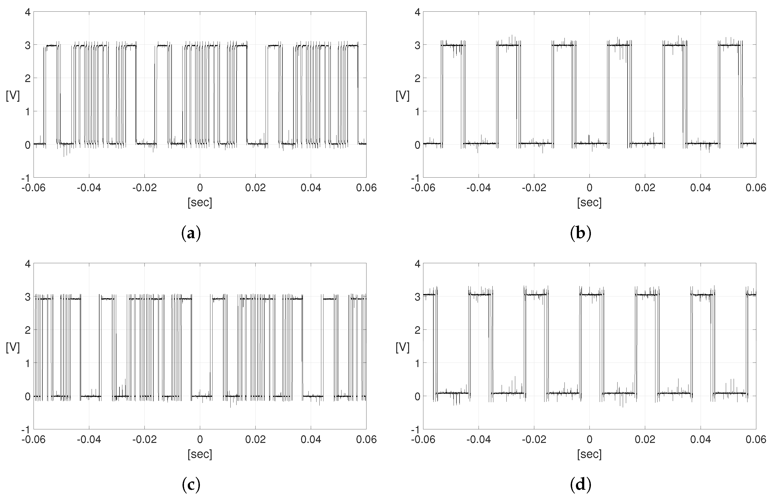
4. Experimental Verification

This section presents selected experimental results for the verification of the theoretical and simulation sections. All waveforms were captured using an R&S RTM3000 oscilloscope and imported to the MATLAB environment for spectral analysis and figure generation. Current and voltage waveforms were acquired using, respectively, Keysight’s current probe N2893A and voltage probe N2791A.
The experimental setup is depicted in Figure 5. The functional performance of the proposed inverter was investigated using the SiC-MOSFET-based laboratory prototype shown in Figure 5a. As can be seen, the proposed inverter was implemented using two-layer 100 mm × 100 mm PCB. For testing flexibility, the load, inductors, and DC source were kept external to the switching circuit and were interfaced to the inverter via designated connectors. A two-layer PCB arrangement was chosen such that the gate driver boards connect perpendicularly to the motherboard through connectors residing adjacent to the MOSFET’s source and drain terminals. As with the simulation, the current source was implemented using a laboratory DC voltage source with a magnitude of 15 V connected in series with a 100 mH choke inductor. The experimental parameters are summarised in Table 4.
Inductor current balancing was maintained using the scheme depicted in Section 2.2. To this end, measurements of the load voltage and inductor currents were acquired using, respectively, LEM’s current transducer L A 55 - P and voltage transducer L V 25 - P . The acquired measurements were then fed to the ADC module of a TI F28379D evaluation board, wherein a simple hysteresis control was implemented. In the case of the voltage measurement, additional shift-and-scale circuitry was required to adjust the voltage transducer AC output to the acceptable voltage range at the ADC input. The balancing index was then fed to a PWM modulator to determine, amongst other things, gate signals S 11 , S 14 , S 21 , and S 24 according to (6).
Figure 6 shows the experimental waveforms for the inverter output current i I N V and inductor currents i L 1 and i L 2 . As with the simulation case, i I N V shows five discrete levels. Similar to the simulated inductor currents, i L 1 and i L 2 fluctuate around a 1 A average, although the peak–peak value of both currents is substantially larger than the simulated one. This is an outcome of low-frequency oscillations in the source current and the combined effect of measurement and quantization errors. The measurement errors are a result of sensor errors, shift-and-scale distortions, and EMI emitted by the inverter.
The fluctuating currents reflect the inverter operation and increase the harmonic content of its output current. This can be mitigated by increasing inductances and operating the inverter in a closed-loop mode.
Figure 7 shows the load voltage v o in the time and frequency domains. As depicted in Figure 7a and in accordance with the simulation results illustrated in Section 3, v o features a sinusoidal waveform with low d v / d t and a peak voltage of 30 V . Here again, the 15 V D C is amplified to a 60 V p p output voltage, which emphasis the inverter’s voltage boosting capability.
The normalised harmonic content of v o is shown in Figure 7b,c, which depict, respectively, 100 and 40 lower-order harmonics of the output voltage. As with the simulation results, the largest harmonic component of the output voltage appears at the switching frequency and amounts to 1.65 % of the fundamental amplitude. The load voltage features a THD of 3.7 % , which is higher than the one attained in the simulation model. This is attributed to the larger fluctuations of the inductor currents arising from looser inductor balancing and the control system’s measurement and quantification errors. These fluctuations also impair the symmetry of the inverter current, which, in turn, results in a small DC component, as can be seen in Figure 7b,c.
As can be inferred from Table 1, the following relations hold for the case of zero off-delay.
S 11 = S 14 ¯ , S 12 = S 23 , S 21 = S 24 ¯ , S 22 = S 13
From (11), neglecting the off-delay effect, switches S 11 , S 12 , S 21 , and S 22 provide a complete picture of the inverter switching states and directly reflect the state of the other four switches. Hence, the acquisition of only four gate waveforms is required.
Figure 8 shows the gating signals for switches S 11 , S 12 , S 21 , and S 22 . As described above, neglecting the off-delay effect, these waveforms are identical to, respectively, those of switches S 14 ¯ , S 23 , S 24 ¯ , and S 13 . For probing convenience, all waveforms were measured at the ePWM pins of the TI F28379D controller board.
Gating signals for switches S 11 and S 21 are depicted, respectively, in Figure 8a,c. Corresponding to the analysis given in Section 2.3, these switches, as well as their complementary switches S 14 and S 24 , commutate at the carrier frequency.
The gating signals for switches S 12 and S 22 are shown, respectively, in Figure 8b,d. As can be seen, these switches commutate at a low fundamental frequency. Their twin switches S 23 and S 13 commutate at the same frequency.
To summarise, switches S 11 and S 21 (and hence also switches S 14 and S 24 ) carry half the source current and switch at the high carrier frequency. On the other hand, switches S 12 and S 22 (and hence also switches S 13 and S 23 ) carry the full source current and switch at a low fundamental frequency. This verifies the analysis summarised in Table 2. As the switching loss is proportional to the product of the current flowing through the switch and its switching frequency, the above observations result in a relatively moderate rating for both the HB and non-HB switches.
It is worth pointing out the extra commutation of switches S 12 and S 22 near the zero crossing of the inverter output current. These commutations are an outcome of toggling between the zero and intermediate current states ± I d / 2 . This can be cancelled altogether by applying a conditional switching rule that matches the correct HB switching state to each half-current cycle.

5. Conclusions

In this study, a novel single-phase five-level CSI topology was introduced. The proposed inverter utilizes eight switches and two DC link inductors to generate five distinct current levels at its output. The proposed CSI features a symmetrical structure and operates with the source current evenly divided between its two inductors. By offsetting the inductor currents from a 1:2 ratio to a 1:3 ratio, the proposed circuit can generate seven current levels. Furthermore, the proposed CSI can operate in single-inductor mode while generating the same number of output levels. This, on the other hand, comes with the cost of doubling the inductor current ripple.
An analysis of the inverter’s functional operation was provided alongside its switching states and corresponding conduction paths. A mathematical analysis of the inductor current’s dynamics as well as the algorithm for its balancing was detailed and verified. The balancing of inductor currents is achieved by employing redundant switching states. A mechanism for inductor current balancing was also provided for the case of single-inductor operation.
The proposed inverter employs an HB submodule to reverse the output current’s polarity. As analysed and verified, the four HB switches thus commutate at the low fundamental frequency while carrying the full source current. The four non-HB switches, on the other hand, switch at the high carrier frequency while carrying half the source current. This favourable feature averages the switching loss of the HB and non-HB switches, allowing for a relatively moderate switch rating.
Open-loop inverter operation and a simple hysteresis control for the balancing of inductor currents were verified by both simulation and experimental means. The testing conducted on a fully functioning laboratory prototype showed high correlation with both the theoretical and simulation sections. While the full extent of the inverter’s voltage boosting capabilities can only be assessed through employing a space vector modulation technique, a stationary operating point with a voltage boost ratio of 1 : 4 was demonstrated in both the simulation and the experimental sections.
Future work will focus on closed-loop operation, loss modelling, sizing, and analysis of the inverter voltage boosting capability through a designated modulation scheme.

Author Contributions

Conceptualization, K.J.D.; methodology, K.J.D.; software, M.F.A.; validation, K.J.D. and M.F.A.; formal analysis, K.J.D.; investigation, K.J.D. and M.F.A.; resources, K.J.D.; data curation, M.F.A.; writing—original draft preparation, M.F.A.; writing—review and editing, K.J.D.; visualization, M.F.A.; supervision, K.J.D.; project administration, K.J.D.; funding acquisition, K.J.D. All authors have read and agreed to the published version of the manuscript.

Funding

This research received no external funding.

Data Availability Statement

Data is contained within the article.

Conflicts of Interest

The authors declare no conflict of interest.

Abbreviations

The following abbreviations are used in this manuscript:
AECAluminium electrolytic capacitor
CSICurrent-source inverter
EMElectric machine
EVElectric vehicle
HBH-bridge
MEAMore electric aircraft
MIIModule-integrated inverter
MPPTMaximum power point tracking
PVPhotovoltaic
RBReverse blocking
ROIReturn on investment
THDTotal harmonic distortion
VSIVoltage-source inverter
WBGWide bandgap

References

  1. Akbar, F.; Cha, H.; Do, D.T. CSI7: Novel Three-Phase Current-Source Inverter With Improved Reliability. IEEE Trans. Power Electron. 2021, 36, 9170–9182. [Google Scholar] [CrossRef]
  2. Estévez-Bén, A.A.; López Tapia, H.J.C.; Carrillo-Serrano, R.V.; Rodríguez-Reséndiz, J.; Vázquez Nava, N. A New Predictive Control Strategy for Multilevel Current-Source Inverter Grid-Connected. Electronics 2019, 8, 902. [Google Scholar] [CrossRef]
  3. Guo, X.; Bai, Y.; Wang, B. A Programmable Single-Phase Multilevel Current Source Inverter. IEEE Access 2019, 7, 102417–102426. [Google Scholar] [CrossRef]
  4. Nguyen, T.T.; Cha, H. Five-Level Current Source Inverter With Inductor Cell Using Switching-Cell Structure. IEEE Trans. Ind. Electron. 2022, 69, 6859–6869. [Google Scholar] [CrossRef]
  5. Fidone, G.L.; Migliazza, G.; Carfagna, E.; Benatti, D.; Immovilli, F.; Buticchi, G.; Lorenzani, E. Common Architectures and Devices for Current Source Inverter in Motor-Drive Applications: A Comprehensive Review. Energies 2023, 16, 5645. [Google Scholar] [CrossRef]
  6. Senthilnathan, K.; Annapoorani, I. Multi-Port Current Source Inverter for Smart Microgrid Applications: A Cyber Physical Paradigm. Electronics 2019, 8, 1. [Google Scholar] [CrossRef]
  7. Dai, H.; Torres, R.A.; Gossmann, J.; Lee, W.; Jahns, T.M.; Sarlioglu, B. A Seven-Switch Current-Source Inverter Using Wide Bandgap Dual-Gate Bidirectional Switches. IEEE Trans. Ind. Appl. 2022, 58, 3721–3737. [Google Scholar] [CrossRef]
  8. He, J.; Lyu, Y.; Han, J.; Wang, C. An SVM Approach for Five-Phase Current Source Converters Output Current Harmonics and Common-Mode Voltage Mitigation. IEEE Trans. Ind. Electron. 2020, 67, 5232–5245. [Google Scholar] [CrossRef]
  9. Torres, R.A.; Dai, H.; Lee, W.; Sarlioglu, B.; Jahns, T. Current-Source Inverter Integrated Motor Drives Using Dual-Gate Four-Quadrant Wide-Bandgap Power Switches. IEEE Trans. Ind. Appl. 2021, 57, 5183–5198. [Google Scholar] [CrossRef]
  10. Migliazza, G.; Buticchi, G.; Carfagna, E.; Lorenzani, E.; Madonna, V.; Giangrande, P.; Galea, M. DC Current Control for a Single-Stage Current Source Inverter in Motor Drive Application. IEEE Trans. Power Electron. 2021, 36, 3367–3376. [Google Scholar] [CrossRef]
  11. Song, Y.; Luo, Y.; Xiong, X.; Blaabjerg, F.; Wang, W. An Improved Submodule Topology of MMC With Fault Blocking Capability Based On Reverse-Blocking Insulated Gate Bipolar Transistor. IEEE Trans. Power Deliv. 2022, 37, 1559–1568. [Google Scholar] [CrossRef]
  12. Kanale, A.; Agarwal, A.; Baliga, B.J.; Bhattacharya, S. Monolithic Reverse Blocking 1.2 kV 4H-SiC Power Transistor: A Novel, Single-Chip, Three-Terminal Device for Current Source Inverter Applications. IEEE Trans. Power Electron. 2022, 37, 10112–10116. [Google Scholar] [CrossRef]
  13. Wang, H.; Mao, W.; Zhao, S.; Du, M.; Zhang, Y.; Zheng, X.; Wang, C.; Zhang, C.; Zhang, J.; Hao, Y. 1.3 kV Reverse-Blocking AlGaN/GaN MISHEMT With Ultralow Turn-On Voltage 0.25 V. IEEE J. Electron Devices Soc. 2021, 9, 125–129. [Google Scholar] [CrossRef]
  14. Madonna, V.; Migliazza, G.; Giangrande, P.; Lorenzani, E.; Buticchi, G.; Galea, M. The Rebirth of the Current Source Inverter: Advantages for Aerospace Motor Design. IEEE Ind. Electron. Mag. 2019, 13, 65–76. [Google Scholar] [CrossRef]
  15. Lazaroiu, A.C.; Gmal Osman, M.; Strejoiu, C.-V.; Lazaroiu, G. A Comprehensive Overview of Photovoltaic Technologies and Their Efficiency for Climate Neutrality. Sustainability 2023, 15, 16297. [Google Scholar] [CrossRef]
  16. Anand, S.; Gundlapalli, S.K.; Fernandes, B.G. Transformer-Less Grid Feeding Current Source Inverter for Solar Photovoltaic System. IEEE Trans. Ind. Electron. 2014, 61, 5334–5344. [Google Scholar] [CrossRef]
  17. Kjaer, S.B.; Pedersen, J.K.; Blaabjerg, F. A review of single-phase grid-connected inverters for photovoltaic modules. IEEE Trans. Ind. Appl. 2005, 41, 1292–1306. [Google Scholar] [CrossRef]
  18. Liu, Y.-F.; Meyer, E.; Liu, X. Recent Developments in Digital Control Strategies for DC/DC Switching Power Converters. IEEE Trans. Power Electron. 2009, 24, 2567–2577. [Google Scholar]
  19. Dai, H.; Jahns, T.M.; Torres, R.A.; Han, D.; Sarlioglu, B. Comparative Evaluation of Conducted Common-Mode EMI in Voltage-Source and Current-Source Inverters using Wide-Bandgap Switches. In Proceedings of the 2018 IEEE Transportation Electrification Conference and Expo (ITEC), Long Beach, CA, USA, 13–15 June 2018; pp. 788–794. [Google Scholar]
  20. Dunlop, E.D.; Halton, D.; Ossenbrink, H.A. 20 years of life and more: Where is the end of life of a PV module? In Proceedings of the Conference Record of the Thirty-first IEEE Photovoltaic Specialists Conference, Lake Buena Vista, FL, USA, 3–7 January 2005; pp. 1593–1596. [Google Scholar] [CrossRef]
  21. Harb, S.; Balog, R.S. Reliability of Candidate Photovoltaic Module-Integrated-Inverter (PV-MII) Topologies—A Usage Model Approach. IEEE Trans. Power Electron. 2013, 28, 3019–3027. [Google Scholar] [CrossRef]
  22. Quan, L.; Wolfs, P. A review of the single phase photovoltaic module integrated converter topologies with three different DC link configurations. IEEE Trans. Power Electron. 2008, 23, 1320–1333. [Google Scholar] [CrossRef]
  23. Castillo, S.J.; Balog, R.S.; Enjeti, P. Predicting capacitor reliability in a module-integrated photovoltaic inverter using stress factors from an environmental usage model. In North American Power Symposium 2010; IEEE: New York, NY, USA, 2010; pp. 1–6. [Google Scholar]
  24. Bazzi, A.M.; Kim, K.A.; Johnson, B.B.; Krein, P.T.; Dominguez-Garcıa, A. Fault impacts on solar power unit reliability. In Proceedings of the 2011 Twenty-Sixth Annual IEEE Applied Power Electronics Conference and Exposition (APEC), Fort Worth, TX, USA, 6–11 March 2011; pp. 1223–1231. [Google Scholar]
  25. Lorenzani, E.; Immovilli, F.; Migliazza, G.; Frigieri, M.; Bianchini, C.; Davoli, M. CSI7: A Modified Three-Phase Current-Source Inverter for Modular Photovoltaic Applications. IEEE Trans. Ind. Electron. 2017, 64, 5449–5459. [Google Scholar] [CrossRef]
  26. De Brito, M.A.G.; Galotto, L.; Sampaio, L.P.; Melo, G.D.A.E.; Canesin, C.A. Evaluation of the Main MPPT Techniques for Photovoltaic Applications. IEEE IEEE Trans. Ind. Electron. 2013, 60, 1156–1167. [Google Scholar] [CrossRef]
  27. Chen, Y.; Smedley, K. Three-Phase Boost-Type Grid-Connected Inverter. IEEE Trans. Power Electron. 2008, 23, 2301–2309. [Google Scholar] [CrossRef]
  28. Singh, A.; Mirafzal, B. An Efficient Grid-Connected Three-Phase Single-Stage Boost Current Source Inverter. IEEE Power Energy Technol. Syst. J. 2019, 6, 142–151. [Google Scholar] [CrossRef]
  29. Mirafzal, B.; Saghaleini, M.; Kaviani, A.K. An SVPWM-Based Switching Pattern for Stand-Alone and Grid-Connected Three-Phase Single-Stage Boost Inverters. IEEE Trans. Power Electron. 2011, 26, 1102–1111. [Google Scholar] [CrossRef]
  30. Guo, X.; Wang, N.; Zhang, J.; Wang, B.; Nguyen, M.K. A Novel Transformerless Current Source Inverter for Leakage Current Reduction. IEEE Access 2019, 7, 50681–50690. [Google Scholar] [CrossRef]
  31. Bai, Z.; Zhang, Z.; Ruan, X. A Natural Soft-Commutation PWM Scheme for Current Source Converter and Its Logic Implementation. IEEE Trans. Ind. Electron. 2011, 58, 2772–2779. [Google Scholar] [CrossRef]
  32. Wang, Z.; Wu, B.; Xu, D.; Cheng, M.; Xu, L. DC-Link Current Ripple Mitigation for Current-Source Grid-Connected Converters Under Unbalanced Grid Conditions. IEEE Trans. Ind. Electron. 2016, 63, 4967–4977. [Google Scholar] [CrossRef]
  33. Sarlioglu, B.; Morris, C.T. More Electric Aircraft: Review, Challenges, and Opportunities for Commercial Transport Aircraft. IEEE Trans. Transp. Electrif. 2015, 1, 54–64. [Google Scholar] [CrossRef]
  34. Mazzanti, G.; Diban, B.; Chiodo, E.; De Falco, P.; Noia, L.P.D. Forecasting the Reliability of Components Subjected to Harmonics Generated by Power Electronic Converters. Electronics 2020, 9, 1266. [Google Scholar] [CrossRef]
  35. Melfi, M.; Sung, A.M.J.; Bell, S.; Skibinski, G.L. Effect of surge voltage risetime on the insulation of low-voltage machines fed by PWM converters. IEEE Trans. Ind. Appl. 1998, 34, 766–775. [Google Scholar] [CrossRef]
  36. Dai, J.; Xu, D.; Wu, B. A Novel Control Scheme for Current-Source-Converter-Based PMSG Wind Energy Conversion Systems. IEEE Trans. Power Electron. 2009, 24, 963–972. [Google Scholar] [CrossRef]
  37. Zhang, J.; Ding, H.; Wang, B.; Guo, X.; Padmanaban, S. Active Power Decoupling for Current Source Converters: An Overview Scenario. Electronics 2019, 8, 197. [Google Scholar] [CrossRef]
  38. Iglesias, I.J.; Acero, J.; Bautista, A. Comparative study and simulation of optimal converter topologies for SMES systems. IEEE Trans. Appl. Supercond. 1995, 5, 254–257. [Google Scholar] [CrossRef]
  39. Wang, Z.; Zheng, Y.; Cheng, M.; Fan, S. Unified Control for a Wind Turbine-Superconducting Magnetic Energy Storage Hybrid System Based on Current Source Converters. IEEE Trans. Magn. 2012, 48, 3973–3976. [Google Scholar] [CrossRef]
  40. Shen, D.; Lehn, P.W. Modeling, analysis, and control of a current source inverter-based STATCOM. IEEE Trans. Power Deliv. 2002, 17, 248–253. [Google Scholar] [CrossRef]
  41. Marignetti, F.; Stefano, R.L.D.; Rubino, G.; Giacomobono, R. Current Source Inverter (CSI) Power Converters in Photovoltaic Systems: A Comprehensive Review of Performance, Control, and Integration. Energies 2023, 16, 7319. [Google Scholar] [CrossRef]
  42. Rodríguez-Benítez, O.M.; Aqui-Tapia, J.A.; Ortega-Velázquez, I.; Espinosa-Pérez, G. Current Source Topologies for Photovoltaic Applications: An Overview. Electronics 2022, 11, 2953. [Google Scholar] [CrossRef]
  43. Wang, Z.; Zou, Z.; Zheng, Y. Design and Control of a Photovoltaic Energy and SMES Hybrid System With Current-Source Grid Inverter. IEEE Trans. Appl. Supercond. 2013, 23, 505–509. [Google Scholar]
  44. Xu, J.; Yang, X.; Zhao, H.; Qiu, J.; Liu, K. An Inductor-Based and Capacitor-Free Bipolar Pulse Converter with Overvoltage Protection. World Electr. Veh. J. 2022, 13, 91. [Google Scholar] [CrossRef]
  45. Yang, X.; Zhao, Z.; Wang, C.; Xu, J.; Liu, K.; Qiu, J. Analysis and Parameter Design of SiC-Based Current Source Inverter (CSI). World Electr. Veh. J. 2022, 13, 187. [Google Scholar] [CrossRef]
  46. Cardoso, J.; Vazquez, N.; Hernandez, C.; Vaquero, J. A Transformerless Single-Phase Current Source Inverter Topology and Control for Photovoltaic Applications. Energies 2018, 11, 2011. [Google Scholar] [CrossRef]
  47. Dagan, K.J.; Zuckerberger, A.; Rabinovici, R. Fourth-Arm Common-Mode Voltage Mitigation. IEEE Trans. Power Electron. 2016, 31, 1401–1407. [Google Scholar] [CrossRef]
  48. Migliazza, G.; Lorenzani, E.; Immovilli, F.; Buticchi, G. Single-Phase Current Source Inverter with Reduced Ground Leakage Current for Photovoltaic Applications. Electronics 2020, 9, 1618. [Google Scholar] [CrossRef]
  49. Braga, H.A.C.; Barbi, I. A new technique for parallel connection of commutation cells: Analysis, design, and experimentation. IEEE Trans. Power Electron. 1997, 12, 387–395. [Google Scholar] [CrossRef]
  50. Bai, Z.; Zhang, Z. Conformation of Multilevel Current Source Converter Topologies Using the Duality Principle. IEEE Trans. Power Electron. 2008, 23, 2260–2267. [Google Scholar] [CrossRef]
  51. Antunes, F.L.M.; Braga, H.A.C.; Barbi, I. Application of a generalized current multilevel cell to current-source inverters. IEEE Trans. Ind. Electron. 1999, 46, 31–38. [Google Scholar] [CrossRef]
  52. Xiong, Y.; Chen, D.; Yang, X.; Hu, C.; Zhang, Z. Analysis and experimentation of a new three-phase multilevel current-source inverter. In Proceedings of the 2004 IEEE 35th Annual Power Electronics Specialists Conference (IEEE Cat. No.04CH37551), Aachen, Germany, 20–25 June 2004; Volume 1, pp. 548–551. [Google Scholar] [CrossRef]
  53. Bai, Z.-H.; Zhang, Z.-C. Research on topology and PWM method of a single-phase multilevel current-source inverter. Proc. CSEE 2007, 27, 73–77. [Google Scholar]
Figure 1. Schematic of the proposed single-phase five-level current-source inverter.
Electronics 13 01213 g001
Figure 2. Conduction paths for the various output current levels.
Electronics 13 01213 g002
Figure 3. Simulated results for inverter current i I N V and inductor currents i L 1 and i L 2 .
Electronics 13 01213 g003
Figure 4. Simulated results for the load voltage v o in the (a) time domain, (b) frequency domain—100 lower harmonics, and (c) frequency domain—40 lower harmonics.
Electronics 13 01213 g004
Figure 5. Single-phase five-level CSI laboratory setup depicting (a) converter laboratory prototype and (b) schematic of the controller and sensor configuration.
Electronics 13 01213 g005
Figure 6. Experimental results for (a) inverter current i I N V and (b) inductor currents i L 1 (black) and i L 2 (grey).
Electronics 13 01213 g006
Figure 7. Experimental results for load voltage v o in the (a) time domain, (b) frequency domain—100 lower harmonics, and (c) frequency domain—40 lower harmonics.
Electronics 13 01213 g007
Figure 8. Controller board gating signals for switches (a) S 11 , (b) S 12 , (c) S 21 , and (d) S 22 .
Electronics 13 01213 g008
Table 1. Switch states for the various output current levels.
S 11 S 12 S 13 S 14 S 21 S 22 S 23 S 24 V L 1 V L 2 i o
110010100 I d
11000011 v o I d 2
01011010 + v o
0001000100
00111100 v o I d 2
10100101 + v o
101011000 I d
Table 2. Sizing factors.
SwitchesMaximum CurrentSwitching FrequencyRole
S 12 , S 13 , S 22 , S 23 I d f 0 HB
S 11 , S 14 , S 21 , S 24 I d 2 f Δ non-HB
Table 3. Simulation parameter summary.
ParameterValueUnitsComments
f 0 50HzFundamental frequency
f Δ 1050HzCarrier frequency
V s 15 V DC Source voltage
L s 100mHSource inductance
R l o a d 22.5 Ω Load resistance
C f 140uFFilter capacitor
Table 4. Experimental parameter summary.
ParameterValueUnitsComments
f 0 50HzFundamental frequency
f Δ 1050HzCarrier frequency
t d t 0.5 usOff-delay
V s 15 V DC Source voltage
L s , L 1 , L 2 100mHSource and coil inductances
R l o a d 22.5 Ω Load resistance
C f 140uFFilter capacitor
S i C M O S F E T C 3 M 0065100 K Wolfspeed
C u r r e t n p r o b e N 2893 A Keysight
V o l t a g e p r o b e N 2791 A Keysight
C o n t r o l l e r F 28379 D C2000 Delfino MCU
D i o d e C 4 D 10120 D Wolfspeed
C u r r e n t t r a n s d u c e r L A 55 - P LEM
V o l t a g e t r a n s d u c e r L V 25 - P LEM
Disclaimer/Publisher’s Note: The statements, opinions and data contained in all publications are solely those of the individual author(s) and contributor(s) and not of MDPI and/or the editor(s). MDPI and/or the editor(s) disclaim responsibility for any injury to people or property resulting from any ideas, methods, instructions or products referred to in the content.

